Downloaded 56 times

![always @( a )
o = a & b ;
∗∗∗∗∗∗∗∗∗∗∗∗∗∗∗∗∗∗∗∗∗∗∗∗∗∗∗∗
endmodule
module code1c (o , a , b ) ;
output o ;
input a , b ;
reg o ;
always
o = a & b ;
endmodule
Note: All three modules infer a 2-input and gate
1.6.3 CASE STATEMENTS
Full Case
Using the synthesis tool directive //synopsys full case gives more information about the
design to the synthesis tool than is provided to the simulation tool. This particular
directive is used to inform the synthesis tool that the case statement is fully defined,
and that the output assignments for all unused cases are don’t cares. The functionality
between pre- and postsynthesized designs may or may not remain the same when using
this directive. Additionally, although this directive is telling the synthesis tool to use the
unused states as dont cares, this directive will sometimes make designs larger and slower
than designs that omit the full case directive.
In module code4a, a case statement is coded without using any synthesis directives.
The pre- and postsynthesis simulations will match. Module code4b uses a case statement
with the synthesis directive full case. Because of the synthesis directive, the en input is
optimized away during synthesis and left as a dangling input. The pre-synthesis simulator
results of modules code4a and code4b will match the post-synthesis simulation results
of module code4a, but will not match the post-synthesis simulation results of module
code4b.
Listing 1.7: Full Case
// no f u l l c a s e
// Decoder b u i l t from four 3−input and gates
// and two i n v e r t e r s
module code4a (y , a , en ) ;
output [ 3 : 0 ] y ;
input [ 1 : 0 ] a ;
input en ;
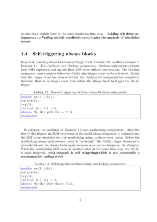
9](https://image.slidesharecdn.com/fpganotes-161031070242/85/FPGA-Coding-Guidelines-9-320.jpg)
![reg [ 3 : 0 ] y ;
always @( a or en ) begin
y = 4 ’ h0 ;
case ({en , a})
3 ’ b1 00 : y [ a ] = 1 ’ b1 ;
3 ’ b1 01 : y [ a ] = 1 ’ b1 ;
3 ’ b1 10 : y [ a ] = 1 ’ b1 ;
3 ’ b1 11 : y [ a ] = 1 ’ b1 ;
endcase
end
endmodule
∗∗∗∗∗∗∗∗∗∗∗∗∗∗∗∗∗∗∗∗∗∗∗∗∗∗∗∗∗∗∗∗∗∗
// f u l l c a s e example
// Decoder b u i l t from four 2−input nor gates
// and two i n v e r t e r s
// The enable input i s dangling ( has been optimized away)
module code4b (y , a , en ) ;
output [ 3 : 0 ] y ;
input [ 1 : 0 ] a ;
input en ;
reg [ 3 : 0 ] y ;
always @( a or en ) begin
y = 4 ’ h0 ;
case ({en , a}) // synopsys f u l l c a s e
3 ’ b1 00 : y [ a ] = 1 ’ b1 ;
3 ’ b1 01 : y [ a ] = 1 ’ b1 ;
3 ’ b1 10 : y [ a ] = 1 ’ b1 ;
3 ’ b1 11 : y [ a ] = 1 ’ b1 ;
endcase
end
endmodule
Parallel Case
Using the synthesis tool directive //synopsys parallel case gives more information about
the design to the synthesis tool than is provided to the simulation tool. This particular
directive is used to inform the synthesis tool that all cases should be tested in parallel,
even if there are overlapping cases which would normally cause a priority encoder to be
inferred. When a design does have overlapping cases, the functionality between pre- and
post-synthesis designs will be different.
10](https://image.slidesharecdn.com/fpganotes-161031070242/85/FPGA-Coding-Guidelines-10-320.jpg)
![caseX
The use of casex statements can cause design problems. A casex treats Xs as ”don’t
cares” if they are in either the case expression or the case items. The problem with casex
occurs when an input tested by a casex expression is initialized to an unknown state. The
pre-synthesis simulation will treat the unknown input as a ”don’t care” when evaluated in
the casex statement. The equivalent post-synthesis simulation will propagate Xs through
the gate-level model, if that condition is tested.
NOTE
• caseZ is same as caseX except ’Z’ treated as dont care.
• ”Aware of a fact that synthesis directives are not recognized by simulators. While
using any synthesis directives makes sure that, it doesn’t lead to pre & post syn-
thesis mismatch”
1.7 FSM
Reference :
• http://www.sunburst-design.com/papers/CummingsICU2002 FSMFundamentals.pdf
• http://www.sunburst-design.com/papers/CummingsSNUG2000Boston FSM.pdf
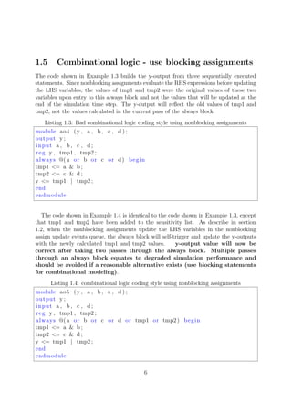
A common classification used to describe the type of an FSM is Mealy and Moore state
machines[2] [3]. A Moore FSM is a state machine where the outputs are only a function
of the present state. A Mealy FSM is a state machine where one or more of the outputs
is a function of the present state and one or more of the inputs.
12](https://image.slidesharecdn.com/fpganotes-161031070242/85/FPGA-Coding-Guidelines-12-320.jpg)
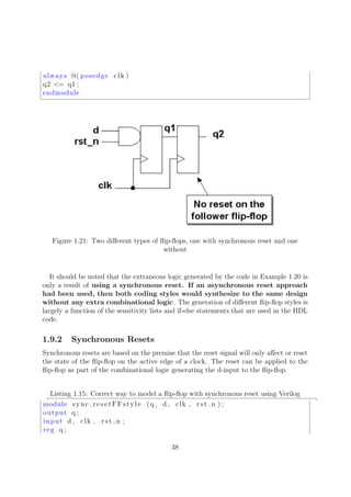
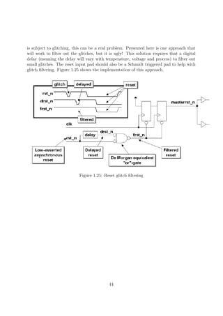
![Figure 1.2: Finite State Machine (FSM) block diagram.
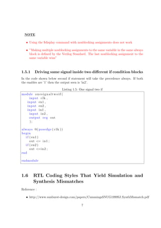
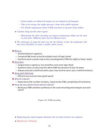
1.7.1 Binary Encoded or Onehot Encoded?
Common classifications used to describe the state encoding of an FSM are Binary (or
highly encoded) and Onehot.
A binary-encoded FSM design only requires as many flip-flops as are needed to uniquely
encode the number of states in the state machine. The actual number of flip-flops required
is equal to the ceiling of the log-base-2 of the number of states in the FSM.
A onehot FSM design requires a flip-flop for each state in the design and only one
flip-flop (the flip-flop representing the current or ”hot” state) is set at a time in a onehot
FSM design. For a state machine with 9- 16 states, a binary FSM only requires 4 flip-
flops while a onehot FSM requires a flip-flop for each state in the design (9-16 flip-flops).
FPGA vendors frequently recommend using a onehot state encoding style because
flip-flops are plentiful in an FPGA and the combinational logic required to implement a
onehot FSM design is typically smaller than most binary encoding styles. Since FPGA
performance is typically related to the combinational logic size of the FPGA design,
onehot FSMs typically run faster than a binary encoded FSM with larger combinational
logic blocks[4].
13](https://image.slidesharecdn.com/fpganotes-161031070242/85/FPGA-Coding-Guidelines-13-320.jpg)
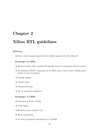
![Figure 1.3: FSM encoding.
Note: When one hot style is used to code FSM without passing // synopsys paral-
lel case directive, synthesis tools always infer priority encoder. This happens because,
there is a possibility that where two bits of the state variable are set and the first state
is given higher priority.
Listing 1.9: one hot
// This l o g i c i n f e r p r i o r i t y encoder
module fsm onehot1
( output reg y , z ,
input wire [ 1 : 0 ] state ) ;
parameter [ 3 : 0 ] IDLE = 0 ,
BBUSY = 1 ,
BWAIT = 2 ,
BFREE = 3;
always @( state ) begin
{y , z} = 2 ’ b0 ;
casez (1 ’ b1)
state [ IDLE ] : z = 1;
state [BBUSY] : y = 1;
endcase
end
endmodule
∗∗∗∗∗∗∗∗∗∗∗∗∗∗∗∗∗∗∗∗∗∗∗∗∗∗∗∗∗∗∗∗∗∗∗∗∗∗∗∗∗∗∗∗∗∗∗∗∗∗∗∗∗∗∗∗∗∗∗∗∗∗∗∗∗∗
14](https://image.slidesharecdn.com/fpganotes-161031070242/85/FPGA-Coding-Guidelines-14-320.jpg)
![// This l o g i c i n f e r p a r a l l e l case
module fsm cc4 fp
( output reg y , z ,
input wire [ 1 : 0 ] state ) ;
parameter [ 3 : 0 ] IDLE = 0 ,
BBUSY = 1 ,
BWAIT = 2 ,
BFREE = 3;
always @( state ) begin
{y , z} = 2 ’b0 ;
casez (1 ’ b1) // synopsys p a r a l l e l c a s e
state [ IDLE ] : z = 1;
state [BBUSY] : y = 1;
endcase
end
endmodule
1.7.2 One Always Block FSM Style (Not Recommended)
One of the most common FSM coding styles in use today is the one sequential always
block FSM coding style. For most FSM designs, the one always block FSM coding style
is more verbose, more confusing and more error prone than a comparable two always
block coding style.
1.7.3 Two Always Block FSM Style
One of the best Verilog coding styles is to code the FSM design using two always blocks,
one for the sequential state register and one for the combinational next-state and com-
binational output logic.
Listing 1.10: fsm design - two always block style
module fsm cc4 2
( output reg gnt ,
input dly , done , req , clk , rst n ) ;
parameter [ 1 : 0 ] IDLE = 2 ’ b00 ,
BBUSY = 2 ’ b01 ,
BWAIT = 2 ’ b10 ,
BFREE = 2 ’ b11 ;
reg [ 1 : 0 ] state , next ;
always @( posedge clk or negedge rst n )
i f ( ! rst n ) state <= IDLE ;
e l s e state <= next ;
15](https://image.slidesharecdn.com/fpganotes-161031070242/85/FPGA-Coding-Guidelines-15-320.jpg)
![• Assignments within the combinational always block are made using Verilog blocking
assignments.
1.7.4 Onehot FSM Coding Style
Efficient (small and fast) onehot state machines can be coded using an inverse case
statement; a case statement where each case item is an expression that evaluates to true
or false.
Listing 1.11: fsm design -onehot style
module fsm cc4 fp
( output reg gnt ,
input dly , done , req , clk , rst n ) ;
parameter [ 3 : 0 ] IDLE = 0 ,
BBUSY = 1 ,
BWAIT = 2 ,
BFREE = 3;
reg [ 3 : 0 ] state , next ;
always @( posedge clk or negedge rst n )
i f ( ! rst n ) begin
state <= 4 ’b0 ;
state [ IDLE ] <= 1 ’b1 ;
end
e l s e state <= next ;
always @( state or dly or done or req ) begin
next = 4 ’ b0 ;
gnt = 1 ’b0 ;
case (1 ’ b1) // ambit synthesis case = f u l l , p a r a l l e l
state [ IDLE ] : i f ( req ) next [BBUSY] = 1 ’b1 ;
e l s e next [ IDLE ] = 1 ’b1 ;
state [BBUSY] : begin
gnt = 1 ’b1 ;
i f ( ! done ) next [BBUSY] = 1 ’ b1 ;
e l s e i f ( dly ) next [BWAIT] = 1 ’b1 ;
e l s e next [BFREE] = 1 ’b1 ;
end
state [BWAIT] : begin
gnt = 1 ’b1 ;
i f ( ! dly ) next [BFREE] = 1 ’ b1 ;
e l s e next [BWAIT] = 1 ’ b1 ;
end
state [BFREE] : begin
17](https://image.slidesharecdn.com/fpganotes-161031070242/85/FPGA-Coding-Guidelines-17-320.jpg)
![i f ( req ) next [BBUSY] = 1 ’ b1 ;
e l s e next [ IDLE ] = 1 ’b1 ;
end
endcase
end
endmodule
1.7.5 Registered FSM Outputs
synthesis results by standardizing the output and input delay constraints of synthesized
modules [5].
FSM outputs are easily registered by adding a third always sequential block to an
FSM module where output assignments are generated in a case statement with case
items corresponding to the next state that will be active when the output is clocked.
Listing 1.12: fsm design -three always blocks w/registered outputs
module fsm cc4 fp
( output reg gnt ,
input dly , done , req , clk , rst n ) ;
parameter [ 3 : 0 ] IDLE = 0 ,
BBUSY = 1 ,
BWAIT = 2 ,
BFREE = 3;
reg [ 3 : 0 ] state , next ;
always @( posedge clk or negedge rst n )
i f ( ! rst n ) begin
state <= 4 ’ b0 ;
state [ IDLE ] <= 1 ’ b1 ;
end
e l s e state <= next ;
always @( state or dly or done or req ) begin
next = 4 ’ b0 ;
gnt = 1 ’b0 ;
case (1 ’ b1) // ambit synthesis case = f u l l , p a r a l l e l
state [ IDLE ] : i f ( req ) next [BBUSY] = 1 ’b1 ;
e l s e next [ IDLE ] = 1 ’b1 ;
state [BBUSY] : begin
gnt = 1 ’b1 ;
i f ( ! done ) next [BBUSY] = 1 ’ b1 ;
e l s e i f ( dly ) next [BWAIT] = 1 ’b1 ;
e l s e next [BFREE] = 1 ’b1 ;
18](https://image.slidesharecdn.com/fpganotes-161031070242/85/FPGA-Coding-Guidelines-18-320.jpg)
![end
state [BWAIT] : begin
gnt = 1 ’b1 ;
i f ( ! dly ) next [BFREE] = 1 ’ b1 ;
e l s e next [BWAIT] = 1 ’ b1 ;
end
state [BFREE] : begin
i f ( req ) next [BBUSY] = 1 ’ b1 ;
e l s e next [ IDLE ] = 1 ’b1 ;
end
endcase
end
endmodule
One or Two or Three always blocks for FSM??
• Use a two always block coding style to code FSM designs with combinational out-
puts. This style is efficient and easy to code and can also easily handle Mealy FSM
designs.
• Use a three always block coding style to code FSM designs with registered outputs.
This style is efficient and easy to code.
1.8 Clock Domain Crossing
Reference :
• http://www.sunburst-design.com/papers/CummingsSNUG2008Boston CDC.pdf
• http://www.sunburst-design.com/papers/CummingsSNUG2001SJ AsyncClk.pdf
1.8.1 Metastability
Metastbility refers to signals that do not have stable 0 or 1 states for some duration
of time at some point during normal operation of a design. In a multi-clock design,
metastability cannot be avoided but the detrimental effects of metastability
can be neutralized.
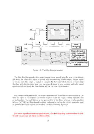
Figure 1.4 shows a synchronization failure that occurs when a signal generated in one
clock domain is sampled too close to the rising edge of a clock signal from a second
clock domain. Synchronization failure is caused by an output going metastable and not
converging to a legal stable state by the time the output must be sampled again.
19](https://image.slidesharecdn.com/fpganotes-161031070242/85/FPGA-Coding-Guidelines-19-320.jpg)

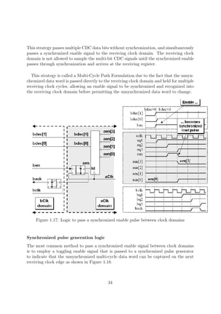
![Figure 1.18: Synchronized pulse generation logic
Figure 1.19: Synchronized enable pulse generation logic and equivalent symbol
1.8.16 Synchronizing counters
When passing multiple signals between clock domains, an important question to ask is,
do I need to sample every value of a signal that is passed from one clock domain to
another? With counters, the answer is frequently, no!
Reference [7] details FIFO design techniques where gray code counters are sampled
between clock domains and intermediate gray count values are often missed. For this
FIFO design, the greater consideration is to make sure that the counters cannot overrun
their boundaries, which could cause missed full and empty flag detection. Even though
the sampled gray count values between clock domains are often missed, the design is
robust and all important gray count values are appropriately sampled. See [7] for details.
Since a valid design might be allowed to skip some count value samples,
can any counter be used to pass count values across a CDC boundary? The
answer is no.
35](https://image.slidesharecdn.com/fpganotes-161031070242/85/FPGA-Coding-Guidelines-35-320.jpg)


![References
[1] http://www.sunburst-design.com/papers/
[2] William I. Fletcher, An Engineering Approach To Digital Design, New Jersey,
Prentice-Hall, 1980.
[3] Zvi Kohavi, Switching And Finite Automata Theory, Second Edition, New York,
McGraw-Hill Book Company, 1978.
[4] The Programmable Logic Data Book, Xilinx, 1994, pg. 8-171.
[5] Clifford E. Cummings, ”Coding And Scripting Techniques For FSM Designs With
Synthesis-Optimized, Glitch- Free Outputs,” SNUG’2000 Boston (Synopsys Users
Group Boston, MA, 2000) Proceedings, September 2000.
[6] Real Intent, Inc. (white paper), Clock Domain Crossing Demystified: The Second
Generation Solution for CDC Verification, February 2008 - www.realintent.com
[7] Clifford E. Cummings, Simulation and Synthesis Techniques
for Asynchronous FIFO Design, SNUG 2002 - www.sunburst-
design.com/papers/CummingsSNUG2002SJ FIFO1.pdf
53](https://image.slidesharecdn.com/fpganotes-161031070242/85/FPGA-Coding-Guidelines-53-320.jpg)

This document outlines RTL coding guidelines to improve hardware simulation using Verilog, focusing on the appropriate use of blocking and nonblocking assignments to prevent race conditions. It provides detailed examples of coding styles, emphasizes the importance of complete sensitivity lists, and discusses the implications of synthesis directives like full case and parallel case on simulation and synthesis mismatches. Adherence to these guidelines is crucial for accurate hardware modeling and synthesis.


![[Deck] What's New in Spark-Iceberg Integration via DSV2.pptx](https://cdn.slidesharecdn.com/ss_thumbnails/deckwhatsnewinspark-icebergintegrationviadsv2-260210005337-25955b12-thumbnail.jpg?width=640&height=640&fit=bounds)
