![Klein Tunneling PHYS 503 Physics Colloquium Fall 2008 9/11 Deepak Rajput Graduate Research Assistant Center for Laser Applications University of Tennessee Space Institute Email: [email_address] Web: http://drajput.com](https://image.slidesharecdn.com/kleintunneling-091216184600-phpapp02/85/Klein-Tunneling-1-320.jpg)
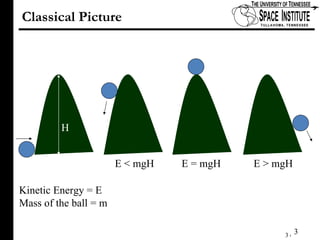

The document discusses Klein tunneling and its applications in quantum mechanics, particularly in graphene. It describes how particles can tunnel through potential barriers despite classical mechanics prohibiting such behavior, emphasizing the difference between electron-like and hole-like states. Additionally, it covers the theoretical implications for bipolar junctions and mentions applications like atomic clocks and tunneling diodes.