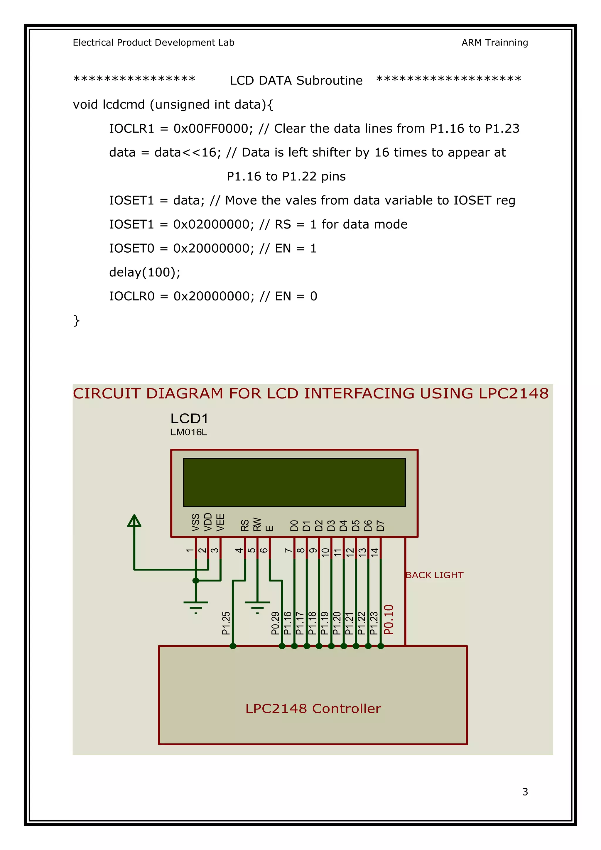
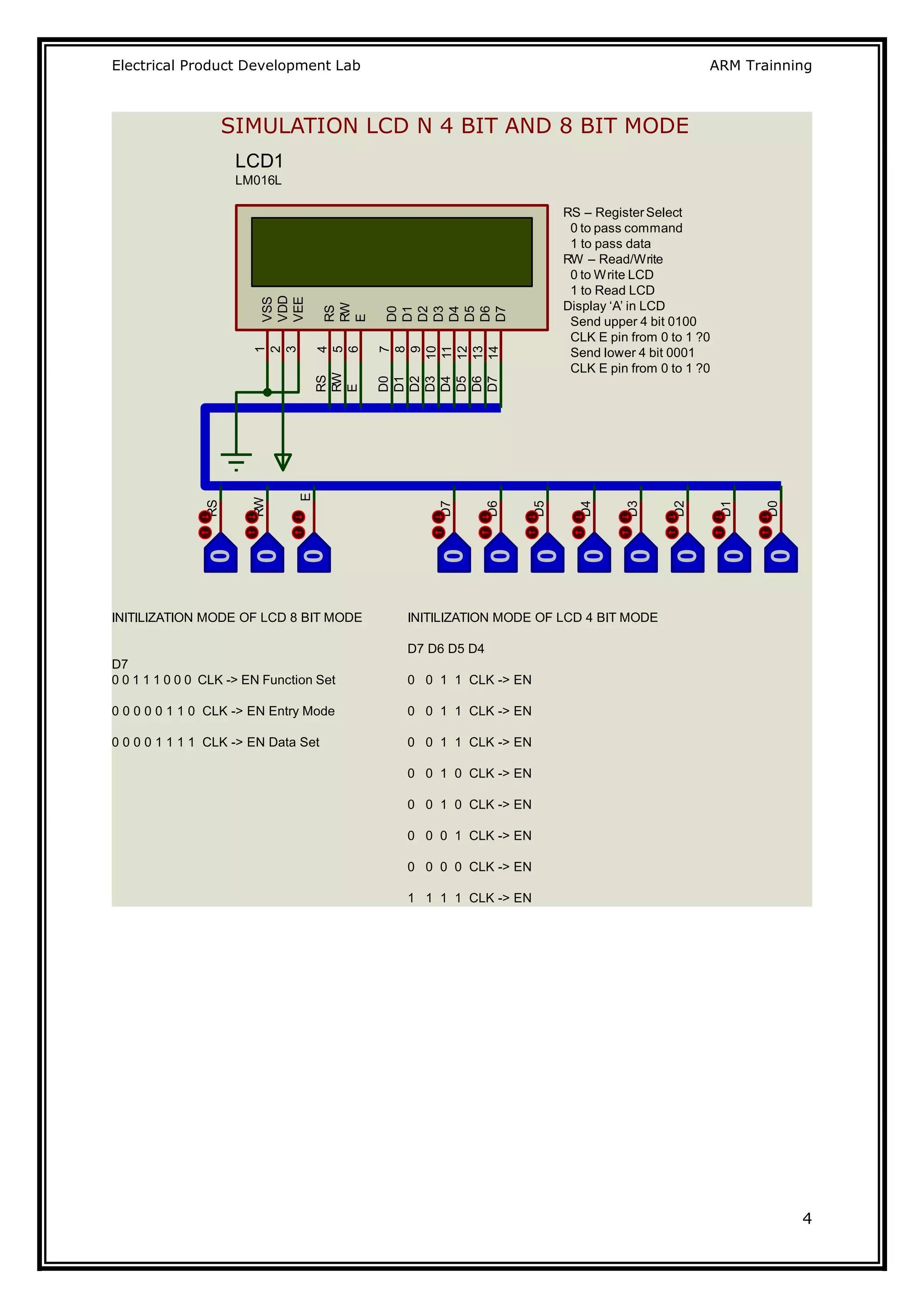
Electrical Product Development Lab ARM Trainning
1
INTERFACING OF 16x2 LCD WITH ARM LPC2148
PROGRAM
# include <lpc21xx.h>
void lcdcmd (unsigned int cmd);
void lcddata (unsigned int data);
void delay (unsigned int itime);
int main()
{
unsigned char array [] = “BIT SATHY”; // Char to be displayed
unsigned int i=0; // initilize i to zero
PINSEL0 = 0x00000000; // All the pins are GPIO pins
PINSEL1 = 0x00000000; // All the pins are GPIO pins
PINSEL2 = 0x00000000; // All the pins are GPIO pins
IODIR0 = 0x20000400; // P0.10 (BC) B.Light, P0.29 – EN as O/P
IODIR1 = 0x02FF0000; // P1.25 – RS and P1.16 to P1.23 as data
pins for D0 – D7 as output
IOCLR0 = 0x00000400; // P0.10 send low value to B.Light
lcdcmd (0x30); // 16x2 LCD with 5x7 matrix mode
delay(100);
lcdcmd (0x06); // Increment cursor with right shift
delay(100);
lcdcmd (0x01); // Clear display screen
delay(100);
lcdcmd (0x0e); // Display ON Cursor ON
delay(100);
lcdcmd (0x80); // First row first position
delay(100);
for(i=0; i<3; i++){
lcd data (array[i]);
Function
prototypes
Electrical Product Development Lab ARM Trainning
2
delay(1000);
}
lcdcmd (0xc0); // 2nd Row first position
delay(100);
for(i=4;i<9;i++){
lcd data (array[i]);
delay(1000);
}
return 0;
} // end of main function
**************** Delay Subroutine ********************
void delay (unsigned int itime){
int i.j;
for(i=0;i<itime;i++)
for(j=0;j<200;j++)
}
**************** LCD CMD Subroutine *******************
void lcdcmd (unsigned int cmd){
IOCLR1 = 0x00FF0000; // Clear the data lines from P1.16 to P1.23
cmd = cmd<<16; // cmd is left shifter by 16 times to appear at
P1.16 to P1.22 pins
IOSET1 = cmd; // Move the vales from cmd variable to IOSET reg
IOCLR1 = 0x02000000; // RS = 0 for command mode
IOSET0 = 0x20000000; // EN = 1
delay(100);
IOCLR0 = 0x20000000; // EN = 0
}
Electrical Product Development Lab ARM Trainning
3
**************** LCD DATA Subroutine *******************
void lcdcmd (unsigned int data){
IOCLR1 = 0x00FF0000; // Clear the data lines from P1.16 to P1.23
data = data<<16; // Data is left shifter by 16 times to appear at
P1.16 to P1.22 pins
IOSET1 = data; // Move the vales from data variable to IOSET reg
IOSET1 = 0x02000000; // RS = 1 for data mode
IOSET0 = 0x20000000; // EN = 1
delay(100);
IOCLR0 = 0x20000000; // EN = 0
}
P1.25
P0.29
P1.16
P1.17
P1.18
P1.19
P1.20
P1.21
P1.22
P1.23
D7
14
D6
13
D5
12
D4
11
D3
10
D2
9
D1
8
D0
7
E
6
RW
5
RS
4
VSS
1
VDD
2
VEE
3
LCD1
LM016L
LPC2148 Controller
P0.10
BACK LIGHT
CIRCUIT DIAGRAM FOR LCD INTERFACING USING LPC2148
Electrical Product Development Lab ARM Trainning
4
D4
D7
D6
D5
D4
RS
RW
E
D7
D6
D5
E
RW
RS
D0
D1
D2
D3
D0
D3
D2
D1
D7
14
D6
13
D5
12
D4
11
D3
10
D2
9
D1
8
D0
7
E
6
RW
5
RS
4
VSS
1
VDD
2
VEE
3
LCD1
LM016L
0
0
0
0
0
0
0
INITILIZATION MODE OF LCD 4 BIT MODE
D7 D6 D5 D4
0 0 1 1 CLK -> EN
0 0 1 1 CLK -> EN
0 0 1 1 CLK -> EN
0 0 1 0 CLK -> EN
0 0 1 0 CLK -> EN
0 0 0 1 CLK -> EN
0 0 0 0 CLK -> EN
1 1 1 1 CLK -> EN
RS – RegisterSelect
0 to pass command
1 to pass data
RW – Read/Write
0 to Write LCD
1 to Read LCD
Display ‘A’ in LCD
Send upper 4 bit 0100
CLK E pin from 0 to 1 ?0
Send lower 4 bit 0001
CLK E pin from 0 to 1 ?0
INITILIZATION MODE OF LCD 8 BIT MODE
D7
0 0 1 1 1 0 0 0 CLK -> EN Function Set
0 0 0 0 0 1 1 0 CLK -> EN Entry Mode
0 0 0 0 1 1 1 1 CLK -> EN Data Set
0
0
0
0
SIMULATION LCD N 4 BIT AND 8 BIT MODE

Program LCD ARM

  • 1.
    Electrical Product DevelopmentLab ARM Trainning 1 INTERFACING OF 16x2 LCD WITH ARM LPC2148 PROGRAM # include <lpc21xx.h> void lcdcmd (unsigned int cmd); void lcddata (unsigned int data); void delay (unsigned int itime); int main() { unsigned char array [] = “BIT SATHY”; // Char to be displayed unsigned int i=0; // initilize i to zero PINSEL0 = 0x00000000; // All the pins are GPIO pins PINSEL1 = 0x00000000; // All the pins are GPIO pins PINSEL2 = 0x00000000; // All the pins are GPIO pins IODIR0 = 0x20000400; // P0.10 (BC) B.Light, P0.29 – EN as O/P IODIR1 = 0x02FF0000; // P1.25 – RS and P1.16 to P1.23 as data pins for D0 – D7 as output IOCLR0 = 0x00000400; // P0.10 send low value to B.Light lcdcmd (0x30); // 16x2 LCD with 5x7 matrix mode delay(100); lcdcmd (0x06); // Increment cursor with right shift delay(100); lcdcmd (0x01); // Clear display screen delay(100); lcdcmd (0x0e); // Display ON Cursor ON delay(100); lcdcmd (0x80); // First row first position delay(100); for(i=0; i<3; i++){ lcd data (array[i]); Function prototypes
  • 2.
    Electrical Product DevelopmentLab ARM Trainning 2 delay(1000); } lcdcmd (0xc0); // 2nd Row first position delay(100); for(i=4;i<9;i++){ lcd data (array[i]); delay(1000); } return 0; } // end of main function **************** Delay Subroutine ******************** void delay (unsigned int itime){ int i.j; for(i=0;i<itime;i++) for(j=0;j<200;j++) } **************** LCD CMD Subroutine ******************* void lcdcmd (unsigned int cmd){ IOCLR1 = 0x00FF0000; // Clear the data lines from P1.16 to P1.23 cmd = cmd<<16; // cmd is left shifter by 16 times to appear at P1.16 to P1.22 pins IOSET1 = cmd; // Move the vales from cmd variable to IOSET reg IOCLR1 = 0x02000000; // RS = 0 for command mode IOSET0 = 0x20000000; // EN = 1 delay(100); IOCLR0 = 0x20000000; // EN = 0 }
  • 3.
    Electrical Product DevelopmentLab ARM Trainning 3 **************** LCD DATA Subroutine ******************* void lcdcmd (unsigned int data){ IOCLR1 = 0x00FF0000; // Clear the data lines from P1.16 to P1.23 data = data<<16; // Data is left shifter by 16 times to appear at P1.16 to P1.22 pins IOSET1 = data; // Move the vales from data variable to IOSET reg IOSET1 = 0x02000000; // RS = 1 for data mode IOSET0 = 0x20000000; // EN = 1 delay(100); IOCLR0 = 0x20000000; // EN = 0 } P1.25 P0.29 P1.16 P1.17 P1.18 P1.19 P1.20 P1.21 P1.22 P1.23 D7 14 D6 13 D5 12 D4 11 D3 10 D2 9 D1 8 D0 7 E 6 RW 5 RS 4 VSS 1 VDD 2 VEE 3 LCD1 LM016L LPC2148 Controller P0.10 BACK LIGHT CIRCUIT DIAGRAM FOR LCD INTERFACING USING LPC2148
  • 4.
    Electrical Product DevelopmentLab ARM Trainning 4 D4 D7 D6 D5 D4 RS RW E D7 D6 D5 E RW RS D0 D1 D2 D3 D0 D3 D2 D1 D7 14 D6 13 D5 12 D4 11 D3 10 D2 9 D1 8 D0 7 E 6 RW 5 RS 4 VSS 1 VDD 2 VEE 3 LCD1 LM016L 0 0 0 0 0 0 0 INITILIZATION MODE OF LCD 4 BIT MODE D7 D6 D5 D4 0 0 1 1 CLK -> EN 0 0 1 1 CLK -> EN 0 0 1 1 CLK -> EN 0 0 1 0 CLK -> EN 0 0 1 0 CLK -> EN 0 0 0 1 CLK -> EN 0 0 0 0 CLK -> EN 1 1 1 1 CLK -> EN RS – RegisterSelect 0 to pass command 1 to pass data RW – Read/Write 0 to Write LCD 1 to Read LCD Display ‘A’ in LCD Send upper 4 bit 0100 CLK E pin from 0 to 1 ?0 Send lower 4 bit 0001 CLK E pin from 0 to 1 ?0 INITILIZATION MODE OF LCD 8 BIT MODE D7 0 0 1 1 1 0 0 0 CLK -> EN Function Set 0 0 0 0 0 1 1 0 CLK -> EN Entry Mode 0 0 0 0 1 1 1 1 CLK -> EN Data Set 0 0 0 0 SIMULATION LCD N 4 BIT AND 8 BIT MODE