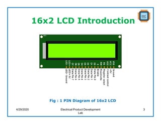
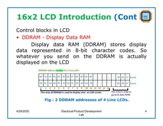
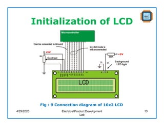
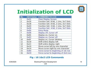
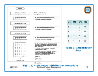
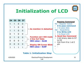
ARM LPC2148 Training
Class - 2
Topic : Introduction to 16x2
LCD, Interfacing with ARM
4/29/2020 Electrical Product Development
Lab
1
Topics
• 16x2 LCD Introduction
• Initialization of LCD
• Simulation of LCD
• Interfacing LCD with ARM
4/29/2020 Electrical Product Development
Lab
2
16x2 LCD Introduction
4/29/2020 Electrical Product Development
Lab
3
Fig : 1 PIN Diagram of 16x2 LCD
16x2 LCD Introduction (Cont..)
4/29/2020 Electrical Product Development
Lab
4
Control blocks in LCD
• DDRAM - Display Data RAM
Display data RAM (DDRAM) stores display
data represented in 8-bit character codes. So
whatever you send on the DDRAM is actually
displayed on the LCD
Fig : 2 DDRAM addresses of 4 Line LCDs.
16x2 LCD Introduction (Cont..)
• CGROM- Character Generator ROM
When we send a ASCII value to DDRAM,
how the character is displayed on LCD? so the
answer is CGROM.
The character generator ROM generates 5 x 8
dot or 5 x 10 dot character patterns from 8-bit
character codes.
It can generate 208 5 x 8 dot character
patterns and 32 5 x 10 dot character patterns
4/29/2020 Electrical Product Development
Lab
5
16x2 LCD Introduction (Cont..)
• CGRAM - Character Generator RAM
As clear from the name, the CGRAM area is used to
create custom characters in LCD.
4/29/2020 Electrical Product Development
Lab
6
Fig : 3 CGRAM addresses of 16x2 LCD
16x2 LCD Introduction (Cont..)
• As you can see in both the code maps, the
character code from 0x00 to 0x07 is occupied
by the CGRAM characters or the user-defined
characters.
• If a user wants to display the fourth custom
character then the code to display it is 0x03
4/29/2020 Electrical Product Development
Lab
7
Fig : 4 Code Maps, the Character Code
16x2 LCD Introduction (Cont..)
4/29/2020 Electrical Product Development
Lab
8
Fig : 5 Character Map for 5x8 Fig : 6 Character Map for 5x10
16x2 LCD Introduction (Cont..)
4/29/2020 Electrical Product Development
Lab
9
Fig : 7 ASCII Character Table
16x2 LCD Introduction (Cont..)
4/29/2020 Electrical Product Development
Lab
10
Fig : 8 Extended ASCII Codes
16x2 LCD Introduction (Cont..)
• BF - Busy Flag
– BF =1 Instruction has being executing
– BF = 0 Instruction is executed successfully
• Instruction Register (IR) and Data Register
(DR) 16 BIT
– IR – 8 Bit
– DR – 8 Bit
4/29/2020 Electrical Product Development
Lab
11
Initialization of LCD
• Two different modes of configuration
– 8 Bit mode
• Operates fast because the data is transferred by
single Enable pulse on EN pin.
• Requires more data lines
– 4 Bit mode
• Requires less data lines
• Operates slow because the data is transferred after
two Enable pulse on EN pin.
4/29/2020 Electrical Product Development
Lab
12
Initialization of LCD
4/29/2020 Electrical Product Development
Lab
13
Fig : 9 Connection diagram of 16x2 LCD
Initialization of LCD
4/29/2020 Electrical Product Development
Lab
14
Fig : 10 16x2 LCD Commands
D4 D5 D6 D7
1 1 0 0
1 1 0 0
1 1 0 0
0 1 0 0
4/29/2020 Electrical Product Development
Lab
15
Fig : 11, 4-Bit mode Initialization Procedure
Table 1: Initialization
Step
Initialization of LCD
4/29/2020 Electrical Product Development
Lab
16
D4 D5 D6 D7
1 1 0 0
1 1 0 0
1 1 0 0
0 1 0 0
0 1 0 0
0 0 0 1
0 0 0 0
1 1 1 1
Table 1: Initialization Step
As mention in datasheet
Function set 4 Bit mode
2 line 5x7 Dots
HEX value – 0x28
Display ON Cursor Blink
HEX value – 0x0F
Passing Command
RS – Register Select
• 0 to pass command
• 1 to pass data
RW – Read/Write
• 0 to Write LCD
• 1 to Read LCD
1. Send Hex Command
• 4 bit binary data to D7
to D4
• CLK from 0 to 1 at E
pin
• .
.
Initialization of LCD
Passing Data to LCD
• RS – Register Select
• 0 to pass command
• 1 to pass data
• RW – Read/Write
• 0 to Write LCD
• 1 to Read LCD
• Display ‘A’ in LCD
• Send upper 4 bit 0100
• CLK E pin from 0 to 1 →0
• Send lower 4 bit 0001
• CLK E pin from 0 to 1 →0
4/29/2020 Electrical Product Development
Lab
17
Initialization of LCD
4/29/2020 Electrical Product Development
Lab
18
Fig : 12, 4-Bit and 8- Bit mode data flow
Simulation of LCD
4/29/2020 Electrical Product Development
Lab
19
Interfacing LCD with ARM
4/29/2020 Electrical Product Development
Lab
20
Assignment
• Write the program to display “ARM” in LCD and
scroll left by 2 times and right by 2 times.
4/29/2020 Electrical Product Development
Lab
21
Thank You
4/29/2020 Electrical Product Development
Lab
22

ARM LCD Interfacing

  • 1.
    ARM LPC2148 Training Class- 2 Topic : Introduction to 16x2 LCD, Interfacing with ARM 4/29/2020 Electrical Product Development Lab 1
  • 2.
    Topics • 16x2 LCDIntroduction • Initialization of LCD • Simulation of LCD • Interfacing LCD with ARM 4/29/2020 Electrical Product Development Lab 2
  • 3.
    16x2 LCD Introduction 4/29/2020Electrical Product Development Lab 3 Fig : 1 PIN Diagram of 16x2 LCD
  • 4.
    16x2 LCD Introduction(Cont..) 4/29/2020 Electrical Product Development Lab 4 Control blocks in LCD • DDRAM - Display Data RAM Display data RAM (DDRAM) stores display data represented in 8-bit character codes. So whatever you send on the DDRAM is actually displayed on the LCD Fig : 2 DDRAM addresses of 4 Line LCDs.
  • 5.
    16x2 LCD Introduction(Cont..) • CGROM- Character Generator ROM When we send a ASCII value to DDRAM, how the character is displayed on LCD? so the answer is CGROM. The character generator ROM generates 5 x 8 dot or 5 x 10 dot character patterns from 8-bit character codes. It can generate 208 5 x 8 dot character patterns and 32 5 x 10 dot character patterns 4/29/2020 Electrical Product Development Lab 5
  • 6.
    16x2 LCD Introduction(Cont..) • CGRAM - Character Generator RAM As clear from the name, the CGRAM area is used to create custom characters in LCD. 4/29/2020 Electrical Product Development Lab 6 Fig : 3 CGRAM addresses of 16x2 LCD
  • 7.
    16x2 LCD Introduction(Cont..) • As you can see in both the code maps, the character code from 0x00 to 0x07 is occupied by the CGRAM characters or the user-defined characters. • If a user wants to display the fourth custom character then the code to display it is 0x03 4/29/2020 Electrical Product Development Lab 7 Fig : 4 Code Maps, the Character Code
  • 8.
    16x2 LCD Introduction(Cont..) 4/29/2020 Electrical Product Development Lab 8 Fig : 5 Character Map for 5x8 Fig : 6 Character Map for 5x10
  • 9.
    16x2 LCD Introduction(Cont..) 4/29/2020 Electrical Product Development Lab 9 Fig : 7 ASCII Character Table
  • 10.
    16x2 LCD Introduction(Cont..) 4/29/2020 Electrical Product Development Lab 10 Fig : 8 Extended ASCII Codes
  • 11.
    16x2 LCD Introduction(Cont..) • BF - Busy Flag – BF =1 Instruction has being executing – BF = 0 Instruction is executed successfully • Instruction Register (IR) and Data Register (DR) 16 BIT – IR – 8 Bit – DR – 8 Bit 4/29/2020 Electrical Product Development Lab 11
  • 12.
    Initialization of LCD •Two different modes of configuration – 8 Bit mode • Operates fast because the data is transferred by single Enable pulse on EN pin. • Requires more data lines – 4 Bit mode • Requires less data lines • Operates slow because the data is transferred after two Enable pulse on EN pin. 4/29/2020 Electrical Product Development Lab 12
  • 13.
    Initialization of LCD 4/29/2020Electrical Product Development Lab 13 Fig : 9 Connection diagram of 16x2 LCD
  • 14.
    Initialization of LCD 4/29/2020Electrical Product Development Lab 14 Fig : 10 16x2 LCD Commands
  • 15.
    D4 D5 D6D7 1 1 0 0 1 1 0 0 1 1 0 0 0 1 0 0 4/29/2020 Electrical Product Development Lab 15 Fig : 11, 4-Bit mode Initialization Procedure Table 1: Initialization Step
  • 16.
    Initialization of LCD 4/29/2020Electrical Product Development Lab 16 D4 D5 D6 D7 1 1 0 0 1 1 0 0 1 1 0 0 0 1 0 0 0 1 0 0 0 0 0 1 0 0 0 0 1 1 1 1 Table 1: Initialization Step As mention in datasheet Function set 4 Bit mode 2 line 5x7 Dots HEX value – 0x28 Display ON Cursor Blink HEX value – 0x0F Passing Command RS – Register Select • 0 to pass command • 1 to pass data RW – Read/Write • 0 to Write LCD • 1 to Read LCD 1. Send Hex Command • 4 bit binary data to D7 to D4 • CLK from 0 to 1 at E pin • . .
  • 17.
    Initialization of LCD PassingData to LCD • RS – Register Select • 0 to pass command • 1 to pass data • RW – Read/Write • 0 to Write LCD • 1 to Read LCD • Display ‘A’ in LCD • Send upper 4 bit 0100 • CLK E pin from 0 to 1 →0 • Send lower 4 bit 0001 • CLK E pin from 0 to 1 →0 4/29/2020 Electrical Product Development Lab 17
  • 18.
    Initialization of LCD 4/29/2020Electrical Product Development Lab 18 Fig : 12, 4-Bit and 8- Bit mode data flow
  • 19.
    Simulation of LCD 4/29/2020Electrical Product Development Lab 19
  • 20.
    Interfacing LCD withARM 4/29/2020 Electrical Product Development Lab 20
  • 21.
    Assignment • Write theprogram to display “ARM” in LCD and scroll left by 2 times and right by 2 times. 4/29/2020 Electrical Product Development Lab 21
  • 22.
    Thank You 4/29/2020 ElectricalProduct Development Lab 22