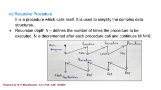
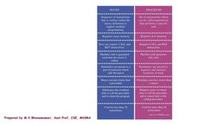
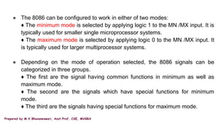
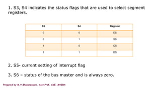
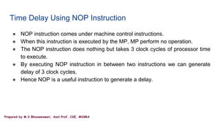
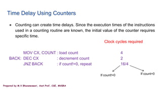
This document discusses various techniques for generating time delays in microprocessors. It describes using NOP instructions, counting loops, and nested loops to create precise delays. With the NOP instruction, each NOP takes a fixed number of clock cycles, allowing delays to be introduced. Counting loops use instructions like DEC and JNZ to iterate a fixed number of times based on an initial count value. Nested loops produce even longer delays by repeating an inner loop multiple times. Examples are provided to calculate delays for known clock speeds and count values.


![Prepared by M.V.Bhuvaneswari, Asst.Prof, CSE, MVGRA
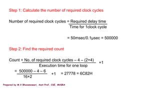
● Assuming operating frequency of 8086 MP is 10MHz then time required for
1clock-cycle = 1/10MHz = 0.1µsec.
● Therefore, time required for execution of a given program with count = 100 is
179.2 µsec (1792 * 0.1)
= [4 + (100 - 1)* (2+16) + (2+4)] = 1792
● Which means 179.2 µsec of delay occurs when the program runs with count
value of 100.](https://image.slidesharecdn.com/ppt-u3-240318195837-99a929a5/85/ppt-U3-Programming-Memory-Interfacing-pptx-8-320.jpg)
![Prepared by M.V.Bhuvaneswari, Asst.Prof, CSE, MVGRA
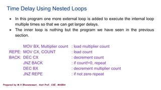
● In delay calculations of nested loops, the delay introduced by inner loop is very large in
comparison with the delay produced by external loop i.e. MOV BX, COUNT , DEC BX and
JNZ instructions.
● Therefore it is not necessary to consider the last loop for external loop delay calculations
separately. The inner loop calculations will remain as it is.
● Clock cycles required to execute the given program is
● For count = 100 and multiplier count = 50, the number of clock cycles required are
[4 + (100 - 1) * (2+16) + (2+4)] * 50
= 89600
[4 + (count - 1)* (2+16) + (2+4)] * Multiplier count](https://image.slidesharecdn.com/ppt-u3-240318195837-99a929a5/85/ppt-U3-Programming-Memory-Interfacing-pptx-12-320.jpg)
![Prepared by M.V.Bhuvaneswari, Asst.Prof, CSE, MVGRA
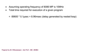
Program: Write an 8086 ALP to generate a delay of 1minute if 8086 system
frequency is 10MHz.
Step 1: Calculate the delay generated by inner loop with maximum count(FFFFH)
Delay generated by inner loop when count = FFFFH = 65535
= [4 + (65535 - 1) * (2+16) + (2+4)] * 0.1µsec
= 117.9622msec
Step 2: Calculate the multiplier count to get delay of 1minute
Multiplier count = required delay/delay provided by inner loop
= 1*60 sec/ 117.9622msec = 509 = 1FDH](https://image.slidesharecdn.com/ppt-u3-240318195837-99a929a5/85/ppt-U3-Programming-Memory-Interfacing-pptx-14-320.jpg)


![Prepared by M.V.Bhuvaneswari, Asst.Prof, CSE, MVGRA
Modular programming
● Modular programming is defined as the process of dividing a larger program
into smaller sub programs[modules].
● Each module is written and tested separately.
● When all modules are tested, they are linked together to form a large
program.
● Three assembly language components are used for the development of
modular program
1) Structure
2) Procedures or subroutines
3) Macros.](https://image.slidesharecdn.com/ppt-u3-240318195837-99a929a5/85/ppt-U3-Programming-Memory-Interfacing-pptx-33-320.jpg)