This document discusses a three-phase power factor controller with minimal output voltage distortion. It presents a single-switch PWM three-phase rectifier that provides a high power factor, wide regulation of the output voltage, and electrical insulation through a high-frequency transformer. The output voltage ripple is eliminated through the use of "one-cycle" pulse width modulation. Additionally, overvoltages across the switch are limited by a lossless clamping circuit, enabling safe operation and high efficiency. The controller achieves a high power factor and low total harmonic distortion of the input current even without duty cycle modulation by operating in discontinuous input current mode.
![S.37.C F O R M E D ' O N D E D U C O U R A N T D'ENTREE ET COMPATIBILTE DES E Q U I P E M E M S
DE CONVERSION D'ENERGIE AVEC LE R E S E A J ELECTRIQUE 1 2
463
THREE-PHASE POWER FACTOR CONTROLLER W I T H M I N I M U M OUTPUT VOLTAGE
DISTORT1O N
U N CONTROLEUR DE FACTEUR DE PUISSANCE TRIPHASE AVEC DISTORTION MINIMALE
DE LA TENSION DE SORTIE
L.
Mdesani , L. Rossetto
G.Spiazzi, P.Tenti
DepPrtment o f Electm~.icsand Informatics
University of Padova
via Gtadenigo 6Ia
35 13 1 Padova Italy
D p r m n of E e t i a Engmeexing
eatet
lcrcl
University of Padova
via Gtadenigo 6Ia
35131 Padova
-
- Italy
Abstract
Rtsumt
On p r h e n t e ici un redresseur triphast P.W.M. a un seul
i n t e v p t e u r Clectronique qui
m e t d'obtenir un facteur
de puissance Cleve. une r e p u g i o n Ctendue de la tension
de sortie et I'isolation Clectrique au moyen d'un
transformateur haute fr6quence. L'ondulation de la
tension de sortie est C l i m n i e g r k e a I'emplol de la
e
technique d e d p u l a t i o n .one cycle". En plus, l s
surtensions aux b o m e s d e I ' i n t e m p t e u r sont linuties par
un circuit k r k t e u r non dissipatif qui permet d'obtenir un
fonctionnement fiable et un rendement plus eleve.
,
,
INTRODUCTION
Pulrcwidth-modulated d G c n are becoming more md mom
popular due to many advanraga: limited ac current dutoruon;
high power factor. no need for low-frequency ac lilten nor
reactive power compaLution; insulation by mcuw of high-fm
qucncy truuformen.
Although mom cxpcnrivtthan conventional mlutions PWM
d f i e n futurc high pomr duuity, wide and fast regulation
clpability and low impact on the rupply. Thua the n a d for ddit i o d compaurting devica in order to comply with rtrndvdr
like IEC 555-2 is rtrongly d u d .
Several r01uti0111 arc p r o p o d in the literrture. both for
ringla and thrraphK appliutiona.
-
Fig1 Bui am-
A ringlc-switch fullycontrolled three-phase rtctiGcr is pns-
which provida high power factor .nd ,,+de dc volhge
hjgh-fraquency hsuhon. owing to
onacyclc
OUtPut
rim1eis * O
Moreover. witch voltage a t r u s is limited by a losslas clampcr
circuit, raulting in ufe opention md high efficiency.
en&,
rcguLtion
Singlaphuc M I U ~ ~ O N11.21 u c mostly brud on ringle
nwitch topologia, which arc c h u p m d provide good 10- m d dcpuforuunca. but thcu power capability doer not exceed fcw
kW.
For higher power Icvclr, threaphuc contiguntiom arc
aomully wd, cithn rtcgdom (inductively-louid) [3] or atcp
up (apoitively-b.dsd)[4].
?hey offer excellent p c r f o m c e a ,
including b i d k t b n d power control, but d for rix fullyoontrollcd nvitc&.; i additin.;, hinafrequency tramformerr
n
must bc ured for irwktion or voltage .d.p.tiun. Syrtana nude
up of r i n g l a p b m b u n b a a .Lo be adopted, which allow
high-fquency inaukrion but rerult in lowcr circuit compaunus.
A d i k m t .ppnrcb hr bcen p ~ t ~ n t c d [SI. where a
in
ringbwbh bead oonfiguntjon ir d to perform a thrab
rcbaac](https://image.slidesharecdn.com/00388529-140129000822-phpapp01/75/power-factor-controller-1-2048.jpg)
![S 37.C INPUT CURRENT WAVEFORMS A N D POWER CONVERSION COMPATIBILTTY WITH ELECTRICAL NETWORK - 2
164
phase (stepup, no power reversal) rectification In spite of the
reduced circuit complexity, a good ac-side behaviour is obtained.
both in terms of power factor and total harmonic distortion
(THD). in this case, however, high-frequency transformers
Also
cannot be used.
In /6/ a three-phase single-switch configuration was p n s entcd. based on an uncontrolled t h n p h a s e rectifier followcd by
a t'uk converfer stage. which allows step-up and stepdown
operation and high-frequency insulation. I t is particularly suitable
for medium-power (kW range) telecommunication applications,
in which power rcvcrsal is not r q u i r c d but high power density
and control simplicity arc prime requirements. The mam
limitations of this solution arc: f m t , high voltage and current
stresses on the switch. which arc typical of single-switch
topologies; second, non-negligible ripple superimposed to the dc
output voltage. arising f o six-pulse operation of the unconrm
trolled rectifier; third, the power loss due to transformer lcakage
inductances, whose energy must be dissipated at M Y turn-off
commutation of the switch.
T i paper demonstrata that these latter dravhacks c
hs
m
actually be m o v e d : the second, by applying the one-cyck
control technique /77; the third, by introducing a suitable
clamping circuit which prevents from OVCrvOItagM across the
switch during the commutations while providing recovery of the
leakage inductance energy.
BASIC CONVERTER EQUATIONS
Thls section recalls the basic convelter equations For a
complek treatment refer to /6]
Assumutions. We assume that:
1) swtching period T, is much smaller than h e period T;
2) voltage ripple on transfer capacitors C, and C d u m g T, is
,
neglipble;
3) line impcdanccs arc purcly inductive;
4) the switch is ideal (no voltage drop, zero lcakage cumnt. no
commutation delay);
5 ) line currents arc zero at the beginning of each switching
cycle (hypothesis of DICM);
6 ) b e voltages arc sinusoidal and symmctncal. given by:
ci =
e sin(wt - 2(i-l)r13)
for i=1,2.3
Owing 1.0 condition 1). we may assume that during a
switching cycle voltages ci rcmain constant at the values:
ci =
sin(8- 2 ( i - l ) ~ / 3 ) for i= 1,2,3
whcrc 8 indicates the angular position of the considered
rwitchmg period w i h the h e period.
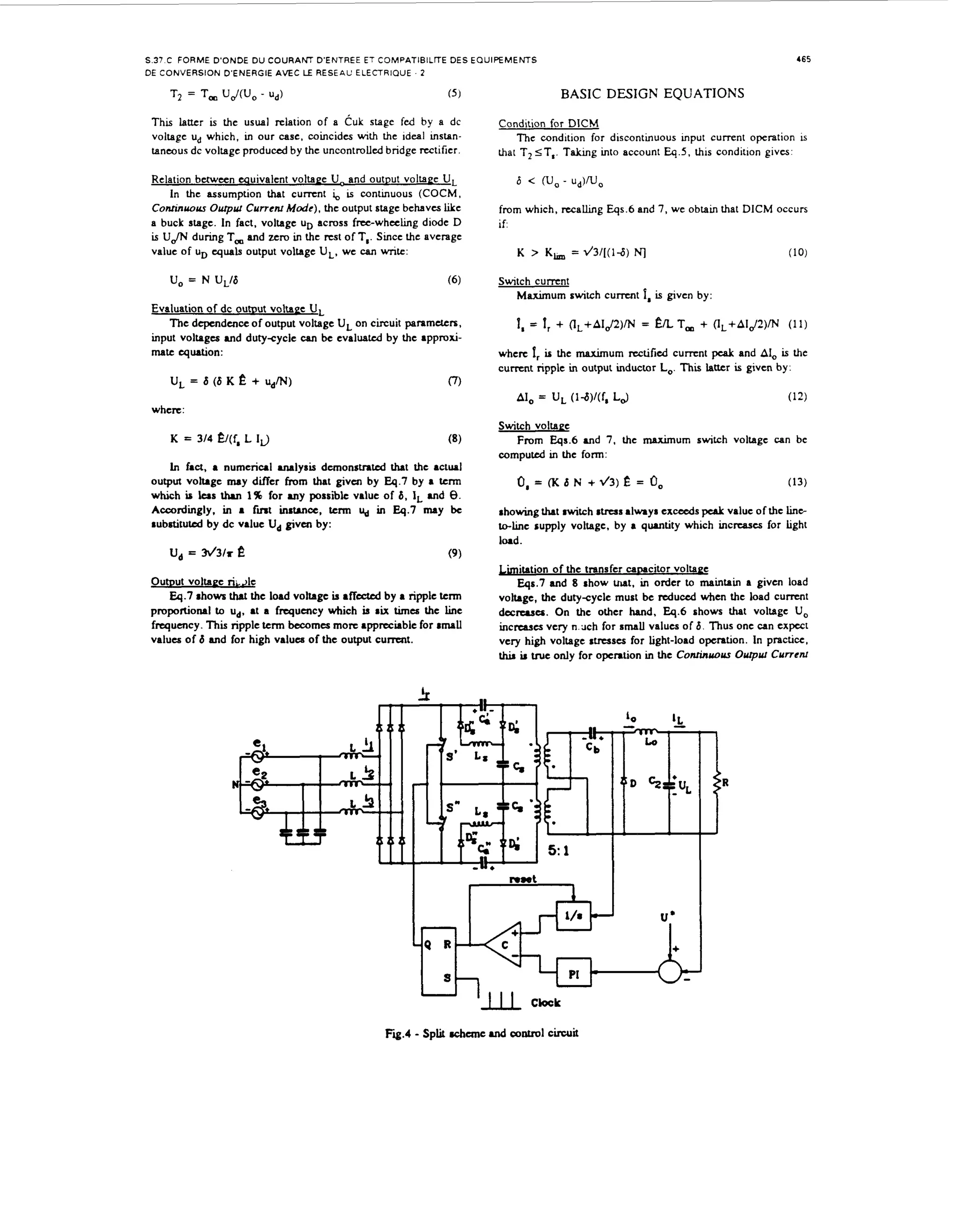
Definitions. With rcfemce ~0Fig.] we defmc:
CONVERTER SCHEME AND
a) Duly cyclr. Lct
PRINCIPLES OF OPERATION
T be the on rime of the switch. duty-cyclc
,
6 is dcfved by:
Fig.1 shows the basic c o n v e e r rchcmc. It includes line
filter inductors L in each supply phase (additional capacitors can
be used for b r filtering), a diode rcctificr, and a Cuk
switching stage with high-frequency tranaformcr.
The circuit behaviour hu been d h c u s d in detail in /]
6.
Here we will only recall aomc basic nape& of operation.
Observe tirat thaf the bcst ac-side performances arc obtained
if the converter M operated in the Disconrinvovr Inpvr Cvrrenr
Mode (DICM), which m u r a high power factor and low THD
even in absence of duty-cyclc modulation. 7his can be cxpkmed
wt reference to the waveforms shown in Fig.2. When the
ih
switch is closed all line currents increase linearly, with a dope
which is p r o p o ~ t i to~the corruponding inst.nt.ncou linc
~ l
voltages. Thus, M rhown in the figure. the peak vdue of a c h
line cumnt during one switching period follow the co-pnding line voltage. Accordingly. one can exnegligible
reactive cunrnts and rnuU harmonic components in the lowfrequency part of the spcctrum /5].
6 = T,n,
b) Tra&onner turn ratio. It M given by:
N = N,/Nb
(2)
c) Equivakw ma&er :apaciror volrage U,. It is the voltage of
the equivalent tranafer capacitor referrcd to the transformer
primary ride:
U = U,
,
+ N U,
Cine c u m [ behaviour.
The ideal h e current waveform during a switching cycle is
s
rhown in Fig.3. The pepk vdue 1i i given by:
ri = q T,L
= 6 ql(f,L),
(4)
thc riae time c q d s , and the duration of the line current pulse
T
U
3
300
2
200
1
100
0
0
-1
-100
-2
-200
-3
-300
1
0
I
4
Fii.2
8
12
16
- Typical ac c u m t mveform
ms
given by:](https://image.slidesharecdn.com/00388529-140129000822-phpapp01/75/power-factor-controller-2-2048.jpg)
![-
166
Mode (COCM).
Instcad. in the case of Disconrinuous 01uprrr Currenr Mode
(DOCM) voltage U, m a i n s constant, k p c c t i v e of load
c u m n t I,, at the value given by Eq.6 in the h i t condition
between DOCM and COCM. Ti h i t value is:
hs
off commutations Moreover. they must avoid overvoltages even
d u m g heavy transients
Instead, mductors L, must provide dc-current balance on
capacitor C,. thus alloulng the clamp voltage to be mamtamcd
at the prcset value In sclectmg L, 11 must be considered also
that its current adds to the on-current m the swtch
From easy computations the commutation tune n s u l t s
where ,1
is the load current whch seis the boundary bctwecn
COCM and DOCM and quls Al.&
while h e clamp voltage variation during the commutation is
pven by:
SPLIT SCHEME
= L a ( , + 1flI2/I2 C, (Uc~mpN U)
1
,]
AUcThe above quations show that voltage stress are quite big.
This CUI affcct the applicability of the proposed scheme,
particularly in the case of 380 V duties.
The voltage stru8 on the switch and primary capacitor CM
be Llved by rpliaing the circuit in two sections, as shown in
Fig.4. In t i scheme the voltage sharing bctwan switches S'
hs
and S and crpciton C', urd C., is c n s u d by a panUel
'
connection of the transformer sccondarics, which involva a
balance of the primary voltages.
It is noticeable that the rolution of Fig.4 does not q u i r e a
prccbc synchronization of the :witch commands.in fact, when
both awitchcr arc c l o u d the vohagu on capaciton C', and C',
bccome equal. due to the voltage balance impored by the tnnrformer. nKn, if one rwitch t m off fvrt its voltage m i n r
ur
near zero, rince tramformer primary voltages match capacitor
voltages. Conversely, w m both witches arc opcn the aame
h
current flow in C', and C', which, again, tend to maintain the
u m e voltage. Whcn one switch turns on ala0 the voltage on the
other nvitch bccoma zcro, due to primary and capacitor voltage
balance. Of coune. in those inatanr~w m only one witch U
h
conducting its c u m t doublcs. due to m.m.f. compenution
betwea~
tramformer windings.
i
valid evcn for the
Note that all the above formulae -n
split scheme, provided that N iI d e f i e d U the tum ratio of each
tnnsformer.
(16)
from which the value of capacitor C, can be chosen.
Assuming now that the voltage variation across C, during
, is the m e given by Eq.16 (quasi-stationary operation).
T
indumr L, can be relcctrd by the quation:
ONE-CYCLE CONTROL
AJ mentioned beforc, operating the convertcr with constant
dutycycle ensum quai-sinusoidal input c u m n u . but the dc
voltage exhibib a l o w - f q u m c y ripple. While the harmonic
content of the input currents cannot be further reduced, the
output voltage waveform CUI be improved by controlling the
duty cycle. For this purpore the onr-rycle control tcchnique r / ]
can profitably be cmploycd.
With t i technique. neglecting dc voltage drop on inductor
ha
Lo,the avenge voltage across diode D is kept qul to the
wanted dc output voltage U
, . For ti purpose. as shown in
'
hs
Fig.4,w1t.p UD on diode D b r e n d and h ~ p k d .
Whcn the
integral r u c h a a proper r e f c m c e (UL*
TJ.the rwitch is
tumcd-off and the in.-ptor b ract. The switch i then turned
s
on synchronously according to the clock signal.Thus wc may
wlilc:
LOSSLESS VOLTAGE CLAMPER
As a l r a d y mentioned, rignificant problana A I ~ I I C
from truuformer pamitics. in particular from the leakage inductanca. In
fact, w m the nvitch U c l o u d , output current i flows through
h
,
the truuformer, giving rire to a cenrin flux lerkrge. Thil flux
h
rcrults in additional voltage aIruru w m the rwitch is tumed
which g i v a :
Off.
In ordcr to limit thac ovcrvoltagcr,
ivoltage
U, =
clamper muat
o d a c m u the truufonncr primvy termiruk. For thia
purpou the nonduripativc p u r i v c ckmpcr rhown in Fig.4 can
bc wd. by which thc a m g y recovered from the tmufonmr
leakage indudurce U rrturned into primvy tnnafer up.citor
C,. 7he behaviour is
U follow.
whal tbe witch U t u d off the t r u u f o n m r primary
ce
to
c u m t m u t m n from the v d u e -@Ithe vrluc + & Sincc
r e v a d time dcpardr on leakage inductu~ce clamping vohmd
age. thia krttr must be ruitlbly higher than tramforma prirmry
voltage. in ordcr to ~ p & d commutation up. On the other
the
hud. ckmper voltage (uroucapacitor C,) annot u a U
cd ,
,
due to thc prt.eaoc of indudor L,,whore avenge voltage drop
i ZCID. n l"
I
u.u
m
witch voltlgccuuIot u a U + U.
cd ,
,
Clam= circuit uanmeterr
Capmiton C, must p w c o t from voltage apika during turn-
In;
7
UD
dt = '
,
U
-T,*T-
bc c
rht output v 0 b . g ~U ~ u I hdcptndcnt of the r i m k Of
,
U
v o h p U&
It U noticable that appliution of o n a c y c k control t Cuko
type convuten may o h rtruh in oacilluory ruponrc of the
input c u m t . In our mnvcltcr, however, thia can never Lppcn
rincc input c u m t r arc discontinuour.
Notc l a d y that onacycle control WO* well .ko i the case
n
of DOCM,where a third voltage Level a p p n wrorr diode D
when c u m t i, vanisha. H o w e r , rince also this voltage is
,
integrucd, UL cquda U* in thia c u e too. Morawcr the dc
,
voltage drop on Lo k cm
oby the PI rcguktor in the
v o w control loop.
SO](https://image.slidesharecdn.com/00388529-140129000822-phpapp01/75/power-factor-controller-4-2048.jpg)
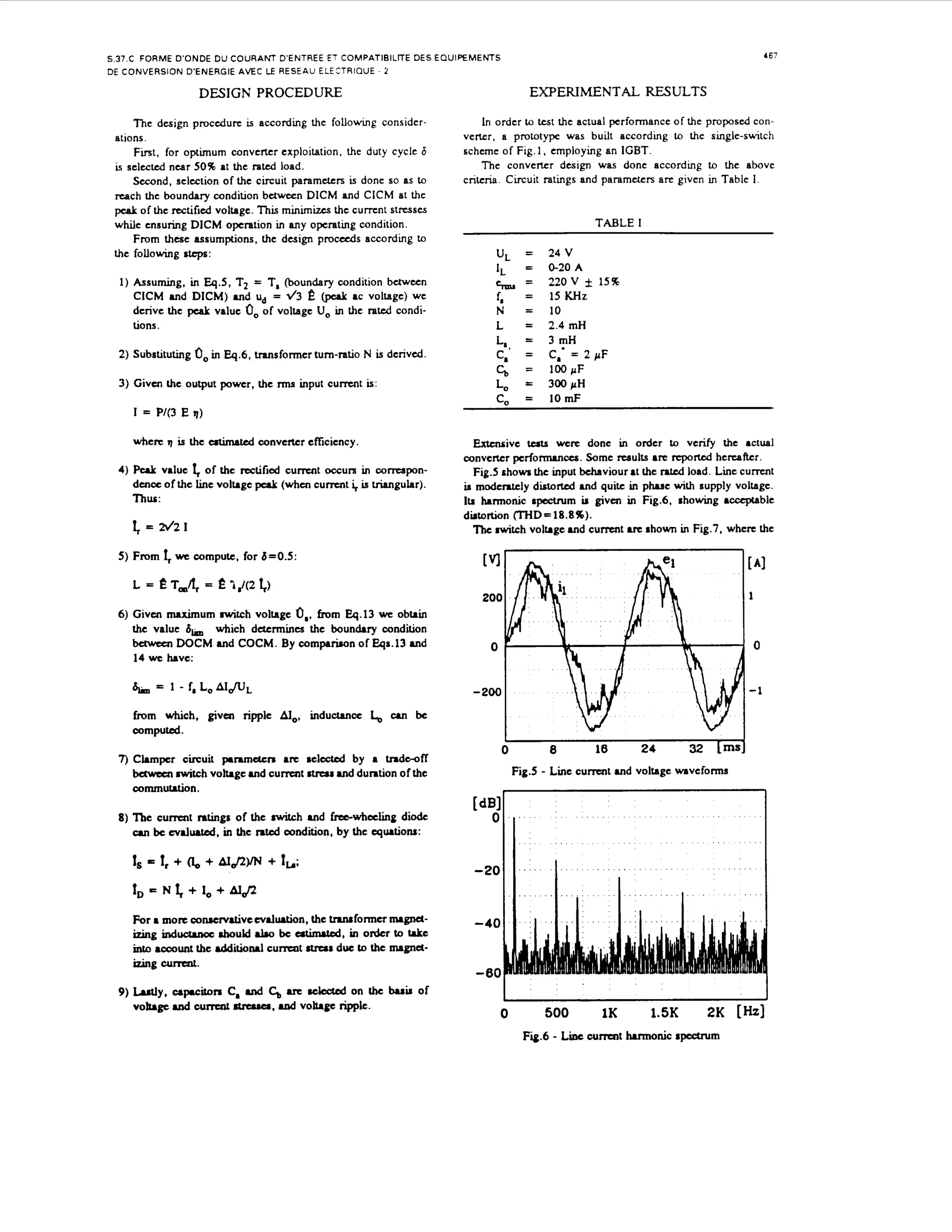
![~
S.37.C INPUT CURRENT WAVEFORMS A N D POWER CONVERSION COMPATIBILITY WITH ELECTRICAL NETWORK. 2
468
effect of the voltage clamper can be ncognized. As anticipated,
voltage stress is h i t 4 to 900 V by the clamper circuit
Lastly, the output voltage spectrum is shown in Fig.8. Owing
to onesyclc control. the harmonic contents is very low. as
r q u d to comply wt most severe specifications of power
ih
supplies for telecommunication quipment.
Acknowlcdgemenk
the
T h e authors would hke to thank Dr.L.Schiavolin. whose
dedicated work made possible prototype development and experimental tcsts.
References
CONCLUSIONS
11 A.R.Rasad. P.D.Ziogas, S.Manias: "A new active power
A single-switch threephase wtificr was presented, which is
capable of high power factor, d u d ac-cumnt and dc-voltage
harmonics, wide range of regulation and high-frquency
insulation.
The wn limitation arises from the high volkgc stress, which
i
can however be overcome by a suitable split circuit arrangement.
Performances CUI be further improved by using onecycle
control, which grutly reduces the output voltage ripple, and by
applying a nondissipative voltage clamper, which incnases
reliability and cftciency.
Due to these benefits, power supplits b u d on Ltus solution
are well :uitd u prc-regulator r u g a in telecommunication
quipmart.
21
31
[4]
(51
US
[q
[7)
factor correction method for single-phase buck-boost ac/dc
converter'. Applid Power Electron~cs
Conference (APEC'92), Boston. February 1992, pp.814-820.
C.A.Cancsin, 1.Barbi: "A unity power factor multiple
isolatd outputs switching mode power supply using a
single switch'. Applied Power Electronic Conferencc
(APEC '91). March 1991, Dallas, pp.430-436.
L.Malcsani, P.Tenti: 'Threephase AClDC PWM converter with :inusoida~ AC c u m t s and minimum fdkr
requirements'. IEEE Trans. on lndustry Applications.
v01.k-23, n.1. 1987, pp.71-TI.
R.Wu, S.B.Dewm, G.R.Slcmon: *Analysis of an a c t o dc
voltage rource converter using PWM with phase and
unptitude control'. IEEE-IAS Annual Meeting, October
1989. San Diego, pp.11561163.
A.R.R.md. P.D.Ziogas, S.Manias: ' A n active power
factor "&on
technique for three phase diode rectifier'.
IEEE T m . on Power Elcctronics, vo1.6, n.1, 1991,
p~ .83-92.
L.Maltsani e al.: 'Singleswitch t h m p h a s c acldc
t
converter with high power factor and wide regulation
capability'. IEEE INTELEC Conf., Washington, October
1992, pp.279-285.
K.M.Smdey. S.Cuk: 'Onecycle control of :witching
converters', IEEE PESC C o d , Boston, June 1991,
pp.888-896.
I
0
26
52
78
104
Fig.7 - M i nwitch and c h p c r waveform
an
P S
1
0
600
Fig.8
1.2k
1.8k
2.4k [b]
- O t u voltage harmonic rpocwm
upt](https://image.slidesharecdn.com/00388529-140129000822-phpapp01/75/power-factor-controller-6-2048.jpg)