The document discusses modelling of DC-DC converters. It describes:
1) DC-DC converters regulate output voltage by varying the duty cycle of switching signals to transistors and diodes.
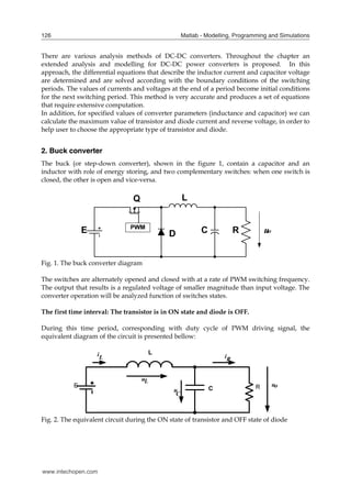
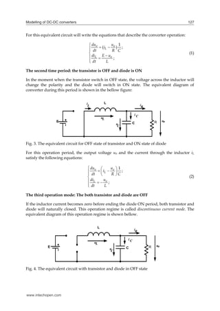
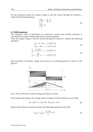
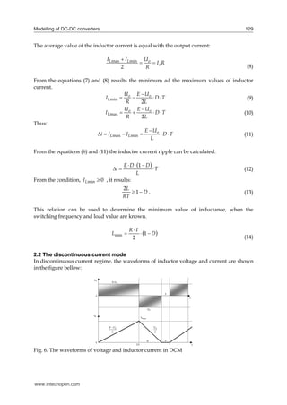
2) Buck and boost converters are analyzed, determining equations for inductor current, capacitor voltage, and minimum inductance for continuous mode.
3) Parameters like maximum current, output ripple, and filtering capacitor value are calculated based on duty cycle, switching frequency, and load.

![Matlab - Modelling, Programming and Simulations
144
As it can be seen at the end of the file, the ed_converter(E,L,C,R,T,D,N,p,type) function is
called. This function is implemented in a file with the same name, and had as arguments the
converter parameters. In the first part of the file are created the buttons that allow to change
the values of the converter parameters. Than, are implemented the functions that solve the
differential equations that describe the converter operation and are calculated the critical
values of inductor for continuous conduction mode operation and value of output voltage.
Also, are defined the plots for output voltage and input current.
The structure of this file is presented bellow:
Listing of function file
function ed_converter(E,L,C,R,T,D,N,p,type);
%create a new figure;
Fig=figure('Name',' DC-DC Converters',...
'Numbertitle','off', 'color', [1, 1, 1]);
% creating 7 text buttons B_T;
txt=['E [V] L[ H] C[ F] R[ohm] T[ s] D N '];
for k=1:7
B_T(k)=uicontrol('Style','text', ...
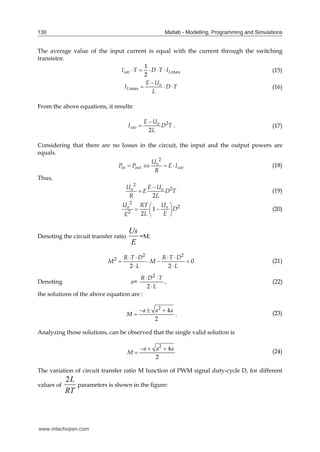
'Units','normalized', ...
'backgroundcolor',[1, 1, 1],...
'Position',[0.91 0.95-0.1.*(k-1) 0.10 0.04], ...
'String',txt((7.*(k-1))+1:7.*k), ...
'Callback','close; ');
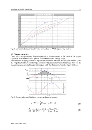
end
% Creating 7 Edit buttons B_E ;
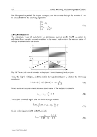
var=['E';'L';'C';'R';'T';'D';'N'];
val=[E;L;C;R;T;D;N];
xc= '=str2num(get(gco,''String''));close;ed_converter(E,L,C,R,T,D,N,p,type)';
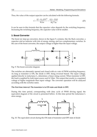
for i=1:7
B_E= uicontrol('Style','edit',...
'Units','normalized',...
'backgroundcolor',[1, 1, 0],...
'Position',[0.91 0.90-0.1*(i-1) 0.10 0.04],...
'String',val(i),...
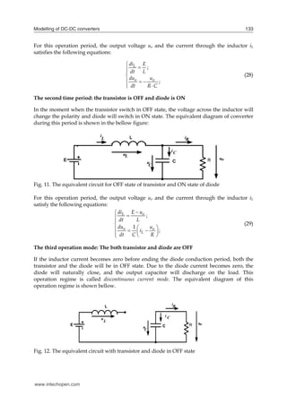
'Callback',cat(2,var(i),xc));
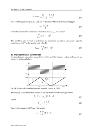
end
%Creating the control buttons for selection of converter type: Buck, Boost or Buck-Boost
Buck=uicontrol('Style','pushbutton',...
'Units','normalized',...
'Position',[0.05 0.01 0.17 0.04],...
'String','Buck',...
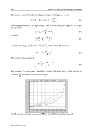
www.intechopen.com](https://image.slidesharecdn.com/dc97-intech-modelingofdcdcconverters-210429201140/85/Dc97-intech-modeling-of-dc_dc_converters-20-320.jpg)
![Modelling of DC-DC converters 145
'backgroundcolor',[0, 1, 0.5],...
'Callback','type=1,close;ed_converter(E,L,C,R,T,D,N,p,type)');
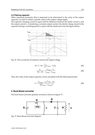
Boost=uicontrol('Style','pushbutton',...
'Units','normalized',...
'Position',[0.25 0.01 0.17 0.04],...
'String','Boost',...
'backgroundcolor',[0, 1, 0.5],...
'Callback','type=2,close;ed_converter(E,L,C,R,T,D,N,p,type)');
Buck_Boost=uicontrol('Style','pushbutton',...
'Units','normalized',...
'Position',[0.45 0.01 0.17 0.04],...
'String','BuckBoost',...
'backgroundcolor',[0, 1, 0.5],...
'Callback','type=3,close;ed_converter(E,L,C,R,T,D,N,p,type)');
%----------------
Bp=uicontrol('Style','pushbutton',...
'Units','normalized',...
'Position',[0.01 0.92 0.19 0.04],...
'String','Steady-State Regime',...
'backgroundcolor',[0, 1, 1],...
'Callback','p=0;close;ed_converter(E,L,C,R,T,D,N,p,type)');
if p==0
set(Bp,'String','Transient Regime');
set(Bp,'Callback','p=1,close;ed_converter(E,L,C,R,T,D,N,p,type)');
end
% When a button is pushed, the callback will call again the function file with the
newer parameters
%Routine for solving the function ec_conv, that describes the converters operation
t=0;
y=[0 0];
for k=1:N
nt=length(t);
t0=(k-1).*T;
tf=t0+D.*T;
ci=y(nt,:);
interval=1;
[t,y]=ode45(@ec_conv,[t0,tf],[ci],[],E,R,L,C,type,interval);
nt=length(t);
%Setting the plots
subplot('Position',[0.10 0.55 0.80 0.35]);
plot(t,y(:,1),'r');grid on;hold on;
subplot('Position',[0.10 0.15 0.80 0.35]);
plot(t,y(:,2),'r');grid on;hold on;
%---------------------interval=2;
t0=(k-1).*T+D.*T;
www.intechopen.com](https://image.slidesharecdn.com/dc97-intech-modelingofdcdcconverters-210429201140/85/Dc97-intech-modeling-of-dc_dc_converters-21-320.jpg)
![Matlab - Modelling, Programming and Simulations
146
tf=k.*T;
ci=y(nt,:);
interval=2;
options=odeset('Events',@conv_ev);
[t,y,te,ye,ie]=ode45(@ec_conv,[t0,tf],[ci],[options],E,R,L,C,type,interval);
nt=length(t);
%-----------------------
subplot('Position',[0.10 0.55 0.80 0.35]);
plot(t,y(:,1),'b');grid on;hold on;
subplot('Position',[0.10 0.15 0.80 0.35]);
plot(t,y(:,2),'b');grid on;hold on;
%----------------------------interval=3;
if te>0;
t0=t(nt);
tf=k.*T;
ci=y(nt,:);
interval=3;
[t,y]=ode45(@ec_conv,[t0,tf],[ci],[],E,R,L,C,type,interval);
%-----------------------
subplot('Position',[0.10 0.55 0.80 0.35]);
plot(t,y(:,1),'g');grid on;hold on;
subplot('Position',[0.10 0.15 0.80 0.35]);
plot(t,y(:,2),'g');grid on;hold on;
%---------------------
end
if (p==0)&(j<N-1)
subplot('Position',[0.10 0.55 0.80 0.35]);
hold off;
end
if (p==0)&(j<N-1)
subplot('Position',[0.10 0.15 0.80 0.35]);
hold off;
end
end
%========================================
subplot('Position',[0.10 0.55 0.80 0.35]);
ylabel(['iL [ A ]']);
switch type;
case 1
Lm=R.*T.*(1-D)./2; %Calculating the minimum value of inductance for Buck Converter
if 2.*L./(R.*T)>=1-D
Uo=E.*D; %Calculating the output voltage in Continuous conduction mode
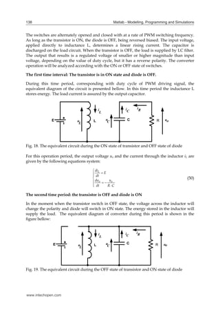
else
www.intechopen.com](https://image.slidesharecdn.com/dc97-intech-modelingofdcdcconverters-210429201140/85/Dc97-intech-modeling-of-dc_dc_converters-22-320.jpg)
![Modelling of DC-DC converters 147
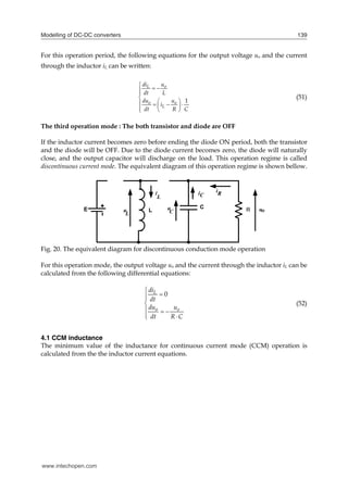
z=0.5.*R.*D.^2.*T./L;
v=0.5.*(sqrt(z.^2+4.*z)-z);
Uo=v.*E; %Calculating the output voltage in Discontinuous conduction mode
end
title(['Buck Converter',' Uo = ',num2str(Uo),' [ V ]',' Lm = ',num2str(Lm),' [ H ]']);
case 2
Lm=R.*T.*D.*(1-D).^2./2; %Calculating the minimum value of inductance for
Boost Converter
di=E.*D.*T./L;
if 2.*L./(R.*T)>=D*(1-D).^2
Uo=E./(1-D); %Calculating the output voltage in Continuous conduction mode
else
v=0.5.*(1+sqrt(1+2.*D.^2.*T.*R./L));
Uo=v.*E; %Calculating the output voltage in Discontinuous conduction mode
end
title(['Boost Converter',' Uo = ',num2str(Uo),' [ V ]',' Lm = ',num2str(Lm),' [ H ]']);
case 3
Lm=R.*T.*(1-D).^2./2, %Calculating the minimum value of inductance
for Buck-Boost Converter
if 2.*L./(R.*T)>=(1-D).^2
Uo=E.*D./(1-D); %Calculating the output voltage in Continuous conduction mode
else
v=D.*sqrt(0.5.*T.*R./L);
Uo=v.*E; %Calculating the output voltage in Discontinuous conduction mode
end
title(['Buck-Boost Converter',' Uo = ',num2str(Uo),' [ V ]',' Lm = ',num2str(Lm),' [ H ]']);
end
subplot('Position',[0.10 0.15 0.80 0.35]);
ylabel(['Uo = uC [ V ]']);
xlabel(['t [ s ]']);
%Function that describes the converters operation
function dy=ec_conv(t,y,E,R,L,C,type,interval);
dy=zeros(2,1);
switch type;
case 1
if interval==1
a=1;b=1;c=1;
www.intechopen.com](https://image.slidesharecdn.com/dc97-intech-modelingofdcdcconverters-210429201140/85/Dc97-intech-modeling-of-dc_dc_converters-23-320.jpg)
![Matlab - Modelling, Programming and Simulations
148
elseif interval==2
a=0;b=1;c=1;
else
a=0;b=0;c=0;
end
case 2
if interval==1
a=1;b=0;c=0;
elseif interval==2
a=1;b=1;c=1;
else
a=0;b=0;c=0;
end
case 3
if interval==1
a=1;b=0;c=0;
elseif interval==2
a=0;b=1;c=1;
else
a=0;b=0;c=0;
end
end
dy(1)=(a.*E-b.*y(2))./L; % Current equation
dy(2)=(c.*y(1)-y(2)./R)./C; % Voltage equation
%===========================================================
function [value,isterminal,direction] =conv_ev(t,y,E,R,L,C,type,interval);
value = y(1); % detect iL = 0
isterminal = 1; % stop the integration
direction = -1; % negative direction
As it can be seen in the converters description, for all types of converters, the equation that
describes the operation has the same shape. The difference consists in the value of the
coefficients. From this reason, the same equations are used for the simulation of the
converters operation and from each converter only the value of a, b, and c coefficients are
set. The equations system is:
1
( )
L o
o o
L
di a E b u
dt L
du u
c i
dt R C
(70)
www.intechopen.com](https://image.slidesharecdn.com/dc97-intech-modelingofdcdcconverters-210429201140/85/Dc97-intech-modeling-of-dc_dc_converters-24-320.jpg)
![Modelling of DC-DC converters 149
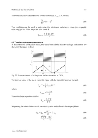
The simulation results of the dc-dc converters are presented in the following figure:
0 0.1 0.2 0.3 0.4 0.5 0.6 0.7 0.8 0.9 1
x 10
-3
-1
0
1
2
3
iL
[
A
]
Buck Converter Uo = 5.3759 [ V ] Lm = 0.000125 [ H ]
0 0.1 0.2 0.3 0.4 0.5 0.6 0.7 0.8 0.9 1
x 10
-3
0
2
4
6
8
10
Uo
=
uC
[
V
]
t [ s ]
Fig. 25. The converters simulation results
As can be seen in the figure, from the upper left side button can be chosen the display mode:
transient, when all the simulated periods are plotted or steady state regime when only the
last simulated period is plotted.
From the right site editing buttons, all of the converter parameters can be set. From the
bottom side it can be selected the desired converter: buck, boost or buck-boost. Also, for
each converter type, the program displays the output voltage value and the minimum
inductance value in order to obtain continuous current mode operation.
6. References
Attaway, S (2009). Matlab: A Practical Introduction to Programming and Problem Solving, 480
pages, Butterworth Heinemann, ISBN 978-0-7506-8762-1, USA
Attia, J. (1999). Electronics and Circuits Analysis using Matlab, 378 pages, CRC Press, ISBN 0-
8493-1176-4, USA
Erickson, R.W. & Macksimovic, D. (2001). Fundamentals of Power Electronics, Second ed., 920
pages, Kluver Academic Publisher, ISBN 0-7923-7270-0, USA
Mohan, N. & Undeland, T.M. (2003). Power Electronics: Converters, Applications and Design.
Third Ed., 802 pages, John Wiley & Sons, ISBN 0-4714-2902-2, USA
Lungu, S. & Pop, O.A. (2006). Modelling of Electronics Circuits, 133 pages, Science Books
House, ISBN 978-973-686-975-4, Romania
Schaffer, R. (2007). Fundamentals of Power Electronics with Matlab, 384 pages, Charles River
Media, ISBN 1-58450-853-3, USA
www.intechopen.com](https://image.slidesharecdn.com/dc97-intech-modelingofdcdcconverters-210429201140/85/Dc97-intech-modeling-of-dc_dc_converters-25-320.jpg)