This document proposes and analyzes a reversible three-phase switching mode rectifier consisting of four active switches. It derives a closed-form pulse width modulation duty cycle control law to achieve sinusoidal input currents, controllable power factor, bidirectional power flow capability, and adjustable DC output voltage without using current sensors. The rectifier is modeled using state space averaging techniques and space vector representation. Both steady-state and small signal analyses are performed. Experimental results demonstrate the rectifier achieves the desired properties and bidirectional power flow. Guidelines for determining component parameters and controller gains are also described.
![Modelling and design of a reversible three-phase
switching mode rectifier
J.-J.Shieh
C.-T. Pan
Z.-J.Cuey
Indexing terms: Three-phase switching mode rect$er, Active switch, Current sensor, Pulse width modulation, Closed-form control law
Abstract: A reversible three-phase switching mode
rectifier consisting of a four-active-switch and
without current sensor is proposed. To achieve
controllable power factor, clean sinusoidal input
current, adjustable DC output voltage, and
bidirectional power flow capability, a closed-form
pulse width modulation (PWM) duty cycle
function is derived. The popularly used state
space averaging technique is extended for
modelling the reversible three-phase four-activeswitch rectifier. The space vector representation
technique is then used to simplify the modelling
process without sacrificing accuracy and valid
frequency range. Both steady-state and small
signal analyses are made. Results show that the
proposed closed-form control law for the rectifier
can indeed achieve the desired property.
Moreover, the rectifier also possesses a
bidirectional power flow capability, which is
useful for many applications. Finally, a prototype
hardware
circuit
was
constructed
and
experimental
results
are
presented
for
demonstration. Guidelines for determining the
LC parameters and the PI controller gains are
described briefly in the text.
1
Introduction
Three-phase diode rectifiers or thyristor rectifiers are
used frequently in many industrial applications which
require a high-power DC supply or as an intermediate
D C link in AC/AC convertors. However, these rectifiers can pollute the AC supply with significant levels of
low frequency harmonics, pulsating input current (electromagnetic interference (EMI)), and excessive VAR
[ 1, 21. With tough regulations and severe economic
restraints, the design of a three-phase switching mode
rectifier which draws nearly sinusoidal three-phase
input currents with unity power factor is very important from the point of view of energy saving and also
to satisfy forthcoming harmonic standards such as
IEEE 519 or IEC 555-2 [3, 41. As a result of recent
rapid progress in high speed power semiconductor
devices, it is now possible to use pulse width modulation (PWM) technology to achieve the above functions.
Several switching mode rectifier topologies have been
proposed to achieve almost sinusoidal waveform with
near-unity power factor [5-91. These rectifiers require
the use of current sensors to correct power factor and/
or eliminate harmonics. From the viewpoints of cost
reduction and enhanced reliability, using fewer active
switches and detector sensors and having higher efficiency are always important goals. Hence, several
switching mode rectifier topologies using fewer switches
have been proposed [lo-121. However, these rectifiers
either require many extra diodes, which incurs more
conduction losses, or are operated in discontinuous
mode, which increases the stress on switches. Also,
existing configurations having a regeneration capability
still require six active switches and some current sensors to shape the desired current. Although Ribeiro et
al. [13] proposed a four-switch convertor with regeneration capability for induction motor drives, it still
required current sensors to improve the input power
factor.
In this paper, a closed-form PWM duty cycle control
for a four-active-switch three-phase switching mode
rectifier is proposed to achieve sinusoidal input current,
controllable power factor, bidirectional capability, and
adjustable D C output voltage without current sensors.
Hence, the hardware circuit can be simplified and the
cost can be reduced.
L
-
L
,
Rs
'c
I
l
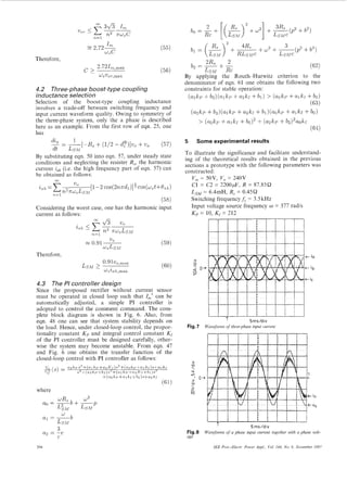
Fig. 1 Main circuit
o
f
switching mode rectifier
0 IEE, 1997
2
Z E E Proceedinfis online no. 19971253
N
the proposed reversible four-switch three-phase
control law
Paper first received 19th August 1996 and in revised form 3rd March
1997
The authors are with the Department of Electrical Engineering, National
Tsing Hua University, Hsinchu, Taiwan, 30043
IEE Proc-Electr. Power Appl., Vol. 144, No. 6, November 1997
Derivation of the closed-form PWM duty cycle
The main circuit of the proposed reversible three-phase
switching mode rectifier (SMR) with sinusoidal input
current and regulated DC output voltage is shown in
389](https://image.slidesharecdn.com/00641915-131014141709-phpapp01/85/modeling-of-three-phase-rectifier-1-320.jpg)
![(iv) t3
-
Substituting eqns. 8 and 9 into eqn. 5 yields the complete state space averaged model as follows:
t4
U, =
d .
(LI+ L,)-%,
dt
-
d .
Lm-2b
dt
d .
- Lm-2,
d
dt
-X
= AX
dt
+ BU
(11)
where
x = [%a
d
1
=ib
i, - -(Uc1 + ' U C 2 )
(4)
dt
R
where R, is the resistance, L is the sum of the per phase
leakage inductance (LI)and mutual inductance (L,) of
the three-phase coupling inductor, C and R are the
capacitance and load resistance, respectively, and vNo
represents the potential difference from N to point 0.
Similarly, the twelve other equivalent circuits and the
corresponding state equations for the remaining time
intervals can be obtained. Hence, by using the state
space averaging technique [ 141 and neglecting the ESR
of the two capacitors, we obtain the state averaged
equation as follows:
ic2
c
+
= c-uc2
0
L+2L,,L
0
0
0
L+2L,,
0 0
L+ZL,,
0
0
0
-
1
0 01
0
0
0
0
0
0 0
-
0
0
-do
-R,
0
-db
%LI+L,
(13)
LSM
A=
--~
R,
LSM
(1
0
-~ 1
0
6LSM
-x, 0
6L;M
0
2
c
J
-
-'(-1+2%--1J)
6LSM
1
(1+2y--s)
GLSlM
LSM
I)
(1+2s--y)
--
--J--l+27,--z)
BLSM
(-z-c-v)
-&(2-"-Y)
LSM
- RC
_
- RIC
_
- -1
2
c
2C
1 0 0 0 0
0 1 0 0 0
0 0 1 0 0
B=-11
L ~ " o o o l o
v
,
dt
CO
-&I I;:I
0 c-
0IT
(12)
'UcZ]
Wcl
0 0 0 0 1
Next, assume input voltages and input currents as follows:
'Ua =
cos wt
Z " 1
2 1,
d
ic
0
'Ub
U=['U,
T
zb
-
v <1
"C2
-
-db
2 , = I , cos(wt - 4)
2,
(5)
where d, and db are duty ratios of switch S , and S3,
respectively.
Assume that the three-phase source is balanced, i.e.
'U,+'Ub+'U,=o
Z,$ib+Zc=o
(6)
Substituting eqn. 6 into eqn. 5 , we obtain
1
'UNO = --[(da
db)'UU,l (1
d,
db)Vu,2]
(7)
3
Now, let
+
+ + +
= I , cos ut
v,1 = vcz =
1
-(I
2
+ y)
I!/ 5 1
z =
-[V,
V
O
cos(4,)
2&
(9)
where x and y denote the time varying part modulation
indices which will be determined later. The duty ratios
of S, and S,, namely d, and d b are defined in sequence
as follows:
1
da -Z 1 - d - _1(1 - Z)
d b E 1 - db = -(I - y)
"-2
2
-
(10)
IEE Psoc.-Elects. Power Appl., Vol. 144. No. 6 , November 1997
-
1
4
1
(18)
f0
Then, by substituting eqn. 18 into eqn. 11 and considering eqns. 16 and 17, the following PWM duty cycle
control law can be obtained explicitly:
-
db =
+-
(
2.ir
3
where V, is the maximum input phase voltage and I,
is the maximum input phase current with phase shift @
included for adjusting power factor.
Assume that the steady state values of vc1and vc2can
be approximated as follows:
Y = -[Vm
-
-
4)
RsIm COS(#^ - 4)]
cos(h)
VO
+ W L S M I ,sin($,
+ W L S M Isin(4b
~
RsIm cos($b
-
d))]
-
4)
(19)
where
4,
wt
30'
&b E w t -
90'
(20)
In addition, the two capacitor state equations can be
obtained by substituting eqn. 19 into the last two rows
of eqn. 11, i.e.
E
-
391](https://image.slidesharecdn.com/00641915-131014141709-phpapp01/85/modeling-of-three-phase-rectifier-3-320.jpg)
![.
1
$cl
+ y i b - 2,)
= -(II:Z,
2
-
vo
R
1
V,
z ( x i a y i b f i c )- (21)
R
At steady state, the DC output voltage is almost constant. Hence
d
d
= -dt c 1 +U&) F 0
(U
.
+
%e2
From eqns. 19-22, one obtains the following relation:
[:
V, = -ImR(Vm COS$
-
1
ImRs)
(23)
Since one of the goals is to eliminate the necessity for a
current sensor, I,* will be considered as a command
signal. If adjustable phase capability is required, 4 can
also be considered as a command signal. Thus, the
desired control law can be rewritten as follows:
II: =
2&
-[V,
+ W L S M I ;sin($,
cos($,)
v,
-
RSIL C O S ( &
a&
7~ = -[Vm
-
q5*)
$*)I
+ W L S M sin(q5b
I~
COS(&,)
-
-
4")
vo
cos($b - $*)I
(24)
If the duty ratios are controlled according to these
equations, the input line current will be forced to be
sinusoidal. Also, by closed-loop implementation, I, can
be controlled automatically and indirectly without
using any current sensor. Fig. 6 shows the schematic
diagram of the control function.
Vb
['U,
'U,]
=Re{[l
= Re{[l
U2
U]V,}
u]is}
u2 ald,}
(29)
Application of the above space vector notation yields
the following compact form:
[Za
Zb
[dl
d2
ZC]
U2
dg]=Re{[l
v
va,b.c
-!-
LSM
R
,
la,b,c
3
+ -Re{i,d,}
d
2
- = --U,
dtuo
I
(31)
c
In the synchronous rotating reference frame, the above
equations can be expressed in terms of direct and quadrature components as follows:
Re
I
d"
z~~-DdId
d
3
Fig.6 Complete block diugmm of the closed-loop control
3
Small signal model of the switching mode
rectifier
For simplicity, states vcl and vc2in eqn. 12 are replaced
with vo (= vcl + vC2),resulting in the following approx-
=
+ -D41q
3
c
-
-V,
2
(34)
Re
C
From eqns. 32-34 one obtains the steady state closedform PWM duty cycle control law corresponding to
eqn. 24 as follows:
1
Dd
=
-(Vm
-
R,I,*
-
wLsMIQ*)
U0
0
-R,
d
-
LSM
dt
0
2d2
C
+-L S1M
where
392
0
1
di
-~
D , = -(RsI,*
LSM
U,
wLsMI;)
(35)
I 4 = -I*m sin 4"
"
(36)
where
I;
I; cos 4"
1
Then, define the following perturbation equations:
Id = Id0 f
.o
-
f,
1,. = I& + I ;
U, =
v,+ 6,
I,*= 140 + f q
I" = I" + I "
4
40
4
(37)
IEE Proc.-Electr. Power Appl.. Vol. 144, No. 6, November 1997](https://image.slidesharecdn.com/00641915-131014141709-phpapp01/85/modeling-of-three-phase-rectifier-4-320.jpg)
![Due to the well-controlled output voltage, eqn. 35 can
be approximated as follows without much influence:
1
-(Vm
Dd
-
R,I,"
- wLsMI,*)
[
V O
Dq
1
-(R,I,*
-
~Lsn/rI,*)
(38)
vo
By substituting eqn. 38 into eqns. 32-34 and linearising
these equations, one obtains the following small signal
model:
where
1
a1
= -(V
m
-
RsI&
-
wLsMI,",)
1
= -(wLsMI,*, - R,I,*,)
vu
1
P1
= T(R,IdO
P2
=
-
+ z9-b
L,,
+ $ (( & ) 2
+ &)')] }
e
EGP(s)
(47)
where
4
Some design guidelines for the switching
mode rectifier
V O
a
2
+ &P
W~SMIqO)
1
E(wLSMId0 + &I@)
(40)
For easy implementation, the resistance of the threephase coupling inductor is neglected (R, = 0) and only
unity power factor is considered, i.e.
I; = I;
I* = 0
4
(41)
Hence, substituting eqn. 41 into eqn. 38, one obtains
the desired control law as follows:
4.7 Output capacitance selection
Selection of the output capacitor involves a trade-off
between rectifier volume and output DC voltage quality, which is dependent on the specific application.
From the previous result of eqn. 23, theoretically, the
output voltage will be pure DC. However, a little ripple
will exist on the output voltage from the switching
action, and this can be estimated from the last row of
eqn. 25 as follows:
where dL@i_1,2,3 the practical PWM duty cycle and
is
can be denoted by the Fourier series as follows:
d@ = di+
1-[1
1
nr
7
n=l
Hence, the simplified small signal model becomes
-
2 cos(2n7rdi) sin(nw,t
+ dni)]
i = 1,2,3
(50)
where wsis switching angular frequency and
On% = tan-'
(43)
where
b - WLSMIk,
Vo
e - WLSMIqO
Vo
V,
p= -
sin(2 n n d , )
1 - cos(2n7rd,)
i = 1,2,3
(51)
Substituting eqns. 50, 51 and 17 into eqn. 49, at steady
state, the ripple component of output voltage vorcan
be obtained:
3
7Jo7=
z=1
V O
(44)
Therefore, applying Laplace transformation to eqn. 43
yields the following transfer functions:
n=l
I,, Ff
nrrJl+(nw,RC)Z
x (1 - 2 ( - 1 ) n
xsin[wt-+(z-I)
cos[zn.rr
e
sin(wt-c-(z-l)
9 )I 1+
9 sin(nw,t+O,,)
1
(52)
where
Em = [(Vm ImR,cosq5- I , w L s ~ s i n 4 ) ~
+(ImR, sin 4 - I,WLSM cos 4 ) 2 ]
(53)
ImR, sin q5 - I,WLSM COS 4
(54)
- I,R,
cos 4 - I,WLSM sin 4
Assuming (ncoSRQ2>> 1 and considering the worst
case, one has the following approximate output ripple
voltage:
E = V,
IEE Proc.-Electr. Power Appl., Vol. 144, No. 6. November 1997
393](https://image.slidesharecdn.com/00641915-131014141709-phpapp01/85/modeling-of-three-phase-rectifier-5-320.jpg)