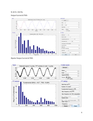
Downloaded 41 times


The document is a lab manual for the Power Electronics course at the Department of Electrical Engineering, SIBAU, covering various experiments such as single-phase and three-phase rectification with different load types, MATLAB/Simulink modeling, and DC motor speed control. It includes detailed procedures, expected outcomes, and analysis based on laboratory experiments conducted in Spring 2017 for BE-VI students. Additionally, it discusses the impact of circuit parameters on performance and provides guidelines for simulations.


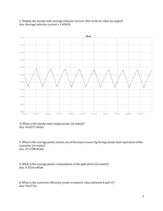
![Bio—chip ] sensor](https://cdn.slidesharecdn.com/ss_thumbnails/biochipsensor-160414183218-thumbnail.jpg?width=640&height=640&fit=bounds)


