Download to read offline
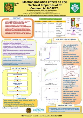

This document summarizes a study on the effects of electron radiation on the electrical properties of commercial MOSFETs. Two types of MOSFETs were irradiated with electron beams at doses from 50-250KGy. For both MOSFET types, drain current increased after irradiation due to generated electron-hole pairs. The P-channel MOSFET exhibited negative threshold voltage shifts and the N-channel MOSFET positive shifts, attributed to increased oxide and interface traps respectively. In conclusion, ionization damage degrades MOSFET performance but helps understand failure mechanisms to improve radiation-hardened designs.