Downloaded 174 times
![13.703 Embedded Systems
Prepared By: Mahesh S
Assist. Professor
MZIST, Chengannur
Page 5
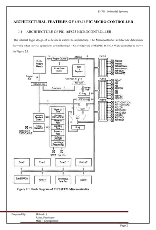
2.3 MEMORY ORGANIZATION
There are three memory blocks in PIC 16F873 Microcontroller [13]. The Program Memory and Data Memory
have separate buses so that concurrent access can occur.
2.3.1 Program Memory Organization
The PIC16F87X devices have a 13-bit program counter capable of addressing an 8K x 14 program memory
space. The PIC 16F873 device has 4K x 14 words of FLASH program memory. Accessing a location above
the physically implemented address will cause a wraparound. The reset vector is at OOOOh and the interrupt
vector is at 0004h.
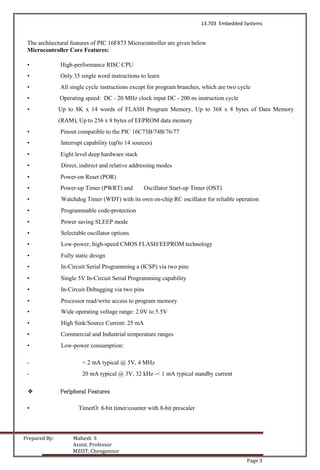
The PIC 16F873 Program memory Map and stack is shown in Figure 2.3.
Figure 2.3 PIC16F873 Program Memory Map And Stack](https://image.slidesharecdn.com/picfullnote-161120164010/85/Pic-full-note-5-320.jpg)
![13.703 Embedded Systems
Prepared By: Mahesh S
Assist. Professor
MZIST, Chengannur
Page 6
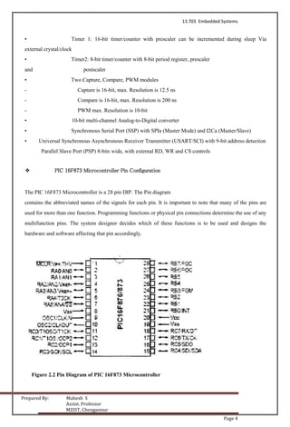
2.3.2 Data Memory Organization
The data memory is partitioned into multiple banks, which contain the General Purpose Registers and the
Special Function Registers. Bits RP1 (STATUS<6>) and RPO (STATUS<5>) are the bank select bits. These
bits are represented in the Table 2.2.
Table 2.2 Bank Select Bits
Each bank extends up to 7Fh (128 bytes). The lower locations of each bank are reserved for the Special
Function Registers. Above the Special Function Registers are General Purpose Registers, implemented as
Static RAM. All implemented banks contain Special Function Registers. Some “high use” Special Function
Registers from one bank may be mirrored in another.
2.3.3 Special Function Registers
Special Function Registers [14] are special elements of RAM, their purpose predefined by the manufacturer.
Each of these registers is named and controls a certain subsystem of MCU. For example: by writing zeros and
ones to the SFR register which controls an I/O port, each of these pins can be designated as input or output
(each register bit corresponds to one of the port pins).
The Special Function Registers are registers used by the CPU and peripheral modules for controlling the
desired operation of the device. These registers are implemented as static RAM. The Special Function
Registers can be classified into two sets; core (CPU) and peripheral.
Status Register
The STATUS register contains the arithmetic status of the ALU, the RESET status and the bank select bits for
data memory. The STATUS register can be the destination for any instruction, as with any other register. If
the STATUS register is the destination for an instruction that affects the Z, DC or C bits, then the write to
these three bits is disabled. These bits are set or cleared according to the device logic. Furthermore, the TO
and PD bits are not writable, therefore, the result of an instruction with the STATUS register as destination](https://image.slidesharecdn.com/picfullnote-161120164010/85/Pic-full-note-6-320.jpg)

![13.703 Embedded Systems
Prepared By: Mahesh S
Assist. Professor
MZIST, Chengannur
Page 9
• Internal or external clock select
• Interrupt on overflow from FFh to OOh
• Edge select for external clock
Timer mode is selected by clearing bit TOCS (OPTION REG<5>). In timer mode, the TimerO module will
increment every instruction cycle (without prescaler). If the TMRO register is written, the increment is
inhibited for the following two instruction cycles. The user can work around this by writing an adjusted value
to the TMRO register. Counter mode is selected by setting bit TOCS (OPTION REG<5>). In counter mode,
TimerO will increment either on every rising or falling edge of pin RA4/T0CKI. The incrementing edge is
determined by the TimerO Source Edge Select bit TOSE (OPTION_REG<4>). Clearing bit TOSE selects the
rising edge. The prescaler is mutually exclusively shared between the TimerO module and the watchdog
timer. The prescaler is not readable or writable
2.5.2 Timer1 Module
The Timerl module is a 16-bit timer/counter consisting of two 8-bit registers (TMR1H and TMR1L), which
are readable and writable. The TMR1 Register pair (TMR1H:TMR1L) increments from OOOOh to FFFFh
and rolls over to OOOOh. The TMR1 Interrupt, if enabled, is generated on overflow, which is latched in
interrupt flag bit TMR1IF (PIR1<0>). This interrupt can be enabled/disabled by setting/clearing TMR1
interrupt enable bit TMR1IE (PIE1<0>). Timerl can operate in one of two modes:
• As a timer
* As a counter
The operating mode is determined by the clock select bit, TMR1CS (T1C0N<1>). In timer mode, Timer 1
increments every instruction cycle. In counter mode, it increments on every rising edge of the external clock
input. Timer 1 can be enabled/disabled by setting/clearing control bit TMRION (T1CON<0>). Timer 1 also
has an internal “reset input”. This reset can be generated by either of the two CCP modules counter mode is
selected by setting bit TMR1CS. In this mode, the timer increments on every rising edge of clock input on pin
RC1/T10SI/CCP2, when bit T10SCEN is set, or on pin RCO/TIOSO/TICKI, when bit T10SCEN is cleared.
Timerl may operate in asynchronous or synchronous mode depending on the setting of the TMR1CS bit.
2.6 ADDRESSABLE UNIVERSAL SYNCHRONOUS
ASYNCHRONOUS RECEIVER TRANSMITTER (USART)
The Universal Synchronous Asynchronous Receiver Transmitter (USART) module is one of the two serial
I/O modules. (USART is also known as a Serial Communications Interface or SCI). The USART [15] can be](https://image.slidesharecdn.com/picfullnote-161120164010/85/Pic-full-note-9-320.jpg)


This document describes the architectural features and peripheral functions of the PIC16F873 microcontroller. It discusses the microcontroller core, which uses a Harvard architecture with separate program and data memory. It then describes the peripheral features including timers, I/O ports, serial communication interfaces, and analog-to-digital converter. Diagrams are included showing the memory map, pin configuration, and block diagrams of timers and serial communication modules. The document provides a detailed overview of the capabilities and operation of the PIC16F873 microcontroller.