
Recommended
Recommended
More Related Content
What's hot
What's hot (19)
Similar to Original NPN Transistor BD135 135 TO-225 New STMicroelectronics
Similar to Original NPN Transistor BD135 135 TO-225 New STMicroelectronics (20)
More from AUTHELECTRONIC
More from AUTHELECTRONIC (20)
Recently uploaded
Recently uploaded (20)
Original NPN Transistor BD135 135 TO-225 New STMicroelectronics
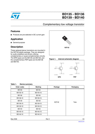
- 1. May 2008 Rev 5 1/9 9 BD135 - BD136 BD139 - BD140 Complementary low voltage transistor Features ■ Products are pre-selected in DC current gain Application ■ General purpose Description These epitaxial planar transistors are mounted in the SOT-32 plastic package. They are designed for audio amplifiers and drivers utilizing complementary or quasi-complementary circuits. The NPN types are the BD135 and BD139, and the complementary PNP types are the BD136 and BD140. Figure 1. Internal schematic diagram 3 2 1 SOT-32 NPN PNP Table 1. Device summary Order codes Marking Package Packaging BD135 BD135 SOT-32 Tube BD135-16 BD135-16 BD136 BD136 BD136-16 BD136-16 BD139 BD139 BD139-10 BD139-10 BD139-16 BD139-16 BD140 BD140 BD140-10 BD140-10 BD140-16 BD140-16 www.st.com
- 2. Contents BD135 - BD136 - BD139 - BD140 2/9 Contents 1 Electrical ratings . . . . . . . . . . . . . . . . . . . . . . . . . . . . . . . . . . . . . . . . . . . . 3 2 Electrical characteristics . . . . . . . . . . . . . . . . . . . . . . . . . . . . . . . . . . . . . 4 2.1 Electrical characteristics (curves) . . . . . . . . . . . . . . . . . . . . . . . . . . . . . . . 5 3 Package mechanical data . . . . . . . . . . . . . . . . . . . . . . . . . . . . . . . . . . . . . 6 4 Revision history . . . . . . . . . . . . . . . . . . . . . . . . . . . . . . . . . . . . . . . . . . . . 8
- 3. BD135 - BD136 - BD139 - BD140 Electrical ratings 3/9 1 Electrical ratings Table 2. Absolute maximum ratings Symbol Parameter Value UnitNPN PNP BD135 BD139 BD136 BD140 VCBO Collector-base voltage (IE = 0) 45 80 -45 -80 V VCEO Collector-emitter voltage (IB = 0) 45 80 -45 -80 V VEBO Emitter-base voltage (IC = 0) 5 -5 V IC Collector current 1.5 -1.5 A ICM Collector peak current 3 -3 A IB Base current 0.5 -0.5 A PTOT Total dissipation at Tc ≤ 25 °C 12.5 W PTOT Total dissipation at Tamb ≤ 25 °C 1.25 W Tstg Storage temperature -65 to 150 °C Tj Max. operating junction temperature 150 °C Table 3. Thermal data Symbol Parameter Max value Unit Rthj-case Thermal resistance junction-case 10 °C/W Rthj-amb Thermal resistance junction-ambient 100 °C/W
- 4. Electrical characteristics BD135 - BD136 - BD139 - BD140 4/9 2 Electrical characteristics (Tcase= 25 °C unless otherwise specified) Table 4. On/off states Symbol Parameter Polarity Test conditions Value Unit Min. Typ. Max. ICBO Collector cut-off current (IE=0) NPN VCB = 30 V VCB = 30 V, TC = 125 °C 0.1 10 µA µA PNP VCB = -30 V VCB = -30 V, TC = 125 °C -0.1 -10 µA µA IEBO Emitter cut-off current (IC=0) NPN VEB = 5 V 10 µA PNP VEB = -5 V -10 µA VCEO(sus) (1) 1. Pulsed: pulse duration = 300 µs, duty cycle 1.5% Collector-emitter sustaining voltage (IB=0) NPN IC = 30 mA BD135 BD139 45 80 V V PNP IC = -30 mA BD136 BD140 -45 -80 V V VCE(sat) (1) Collector-emitter saturation voltage NPN IC = 0.5 A, IB = 0.05 A 0.5 V PNP IC = -0.5 A, IB = -0.05 A -0.5 V VBE (1) Base-emitter voltage NPN IC = 0.5 A, VCE = 2 V 1 V PNP IC = -0.5 A, VCE = -2 V -1 V hFE (1) DC current gain NPN IC = 5 mA, VCE = 2 V IC = 150 mA, VCE = 2 V IC = 0.5 A, VCE = 2 V 25 40 25 250 PNP IC = -5 mA, VCE = -2 V IC = -150 mA, VCE = -2 V IC = -0.5 A, VCE = -2 V 25 40 25 250 hFE (1) hFE groups NPN IC = 150 mA, VCE = 2 V BD139-10 BD135-16/BD139-16 63 100 160 250 PNP IC = -150 mA, VCE = -2 V BD140-10 BD136-16/BD140-16 63 100 160 250
- 5. BD135 - BD136 - BD139 - BD140 Electrical characteristics 5/9 2.1 Electrical characteristics (curves) Figure 2. Safe operating area Figure 3. Derating
- 6. Package mechanical data BD135 - BD136 - BD139 - BD140 6/9 3 Package mechanical data In order to meet environmental requirements, ST offers these devices in ECOPACK® packages. These packages have a lead-free second level interconnect. The category of second level interconnect is marked on the package and on the inner box label, in compliance with JEDEC Standard JESD97. The maximum ratings related to soldering conditions are also marked on the inner box label. ECOPACK is an ST trademark. ECOPACK specifications are available at: www.st.com
- 7. BD135 - BD136 - BD139 - BD140 Package mechanical data 7/9
- 8. Revision history BD135 - BD136 - BD139 - BD140 8/9 4 Revision history Table 5. Document revision history Date Revision Changes 16-Sep-2001 4 22-May-2008 5 Mechanical data has been updated.
- 9. BD135 - BD136 - BD139 - BD140 9/9 Please Read Carefully: Information in this document is provided solely in connection with ST products. STMicroelectronics NV and its subsidiaries (“ST”) reserve the right to make changes, corrections, modifications or improvements, to this document, and the products and services described herein at any time, without notice. All ST products are sold pursuant to ST’s terms and conditions of sale. Purchasers are solely responsible for the choice, selection and use of the ST products and services described herein, and ST assumes no liability whatsoever relating to the choice, selection or use of the ST products and services described herein. No license, express or implied, by estoppel or otherwise, to any intellectual property rights is granted under this document. If any part of this document refers to any third party products or services it shall not be deemed a license grant by ST for the use of such third party products or services, or any intellectual property contained therein or considered as a warranty covering the use in any manner whatsoever of such third party products or services or any intellectual property contained therein. UNLESS OTHERWISE SET FORTH IN ST’S TERMS AND CONDITIONS OF SALE ST DISCLAIMS ANY EXPRESS OR IMPLIED WARRANTY WITH RESPECT TO THE USE AND/OR SALE OF ST PRODUCTS INCLUDING WITHOUT LIMITATION IMPLIED WARRANTIES OF MERCHANTABILITY, FITNESS FOR A PARTICULAR PURPOSE (AND THEIR EQUIVALENTS UNDER THE LAWS OF ANY JURISDICTION), OR INFRINGEMENT OF ANY PATENT, COPYRIGHT OR OTHER INTELLECTUAL PROPERTY RIGHT. UNLESS EXPRESSLY APPROVED IN WRITING BY AN AUTHORIZED ST REPRESENTATIVE, ST PRODUCTS ARE NOT RECOMMENDED, AUTHORIZED OR WARRANTED FOR USE IN MILITARY, AIR CRAFT, SPACE, LIFE SAVING, OR LIFE SUSTAINING APPLICATIONS, NOR IN PRODUCTS OR SYSTEMS WHERE FAILURE OR MALFUNCTION MAY RESULT IN PERSONAL INJURY, DEATH, OR SEVERE PROPERTY OR ENVIRONMENTAL DAMAGE. ST PRODUCTS WHICH ARE NOT SPECIFIED AS "AUTOMOTIVE GRADE" MAY ONLY BE USED IN AUTOMOTIVE APPLICATIONS AT USER’S OWN RISK. Resale of ST products with provisions different from the statements and/or technical features set forth in this document shall immediately void any warranty granted by ST for the ST product or service described herein and shall not create or extend in any manner whatsoever, any liability of ST. ST and the ST logo are trademarks or registered trademarks of ST in various countries. Information in this document supersedes and replaces all information previously supplied. The ST logo is a registered trademark of STMicroelectronics. All other names are the property of their respective owners. © 2008 STMicroelectronics - All rights reserved STMicroelectronics group of companies Australia - Belgium - Brazil - Canada - China - Czech Republic - Finland - France - Germany - Hong Kong - India - Israel - Italy - Japan - Malaysia - Malta - Morocco - Singapore - Spain - Sweden - Switzerland - United Kingdom - United States of America www.st.com