Original N-channel 650 V 0.230 Ohm 12 A MDmesh V Power MOSFET in DPAK DPAK ST...AUTHELECTRONIC
Original N-channel 650 V 0.230 Ohm 12 A MDmesh V Power MOSFET in DPAK DPAK STF16N65M5 16N65M5 16N65 710V 12A TO-220FP New STMicroelectronics
https://authelectronic.com/original-n-channel-650-v-0-230-ohm-12-a-mdmesh-v-power-mosfet-in-dpak-dpak-stf16n65m5-16n65m5-16n65-710v-12a-to-220fp-new-stmicroelectronics
Original N-Channel Power MOSFET IRF1010EPBF IRF1010 1010 60V 84A TO-220 New I...AUTHELECTRONIC
Original N-Channel Power MOSFET IRF1010EPBF IRF1010 1010 60V 84A TO-220 New International Rectifier
https://authelectronic.com/original-n-channel-power-mosfet-irf1010epbf-irf1010-1010-60v-84a-to-220-new-international-rectifier
Dienhathe.com miniature circuit breakersDien Ha The
Siemens,
Catalog Thiết Bị Điện Siemens, Catalog Thiết Bị Điện,
Catalog Phụ Kiện Siemens, Catalog Phụ Kiện,
Catalog Siemens, Catalog,
http://dienhathe.com,
Chi tiết các sản phẩm khác của Siemens tại https://dienhathe.com
Xem thêm các Catalog khác của Siemens tại https://dienhathe.info
Để nhận báo giá sản phẩm Siemens vui lòng gọi: 0907.764.966
ICL7660 Monolithic CMOS Voltage ConvertersGeorgage Zim
ICL7660 and ICL7660A contain all the necessary circuitry to complete a negative voltage converter, with the exception of 2 external capacitors which may be inexpensive 10μF polarized electrolytic types. Please visit for more information http://www.intersil.com/en/products/power-management/isolated-power/charge-pumps/ICL7660.html
Welcome to WIPAC Monthly the magazine brought to you by the LinkedIn Group Water Industry Process Automation & Control.
In this month's edition, along with this month's industry news to celebrate the 13 years since the group was created we have articles including
A case study of the used of Advanced Process Control at the Wastewater Treatment works at Lleida in Spain
A look back on an article on smart wastewater networks in order to see how the industry has measured up in the interim around the adoption of Digital Transformation in the Water Industry.
About
Indigenized remote control interface card suitable for MAFI system CCR equipment. Compatible for IDM8000 CCR. Backplane mounted serial and TCP/Ethernet communication module for CCR remote access. IDM 8000 CCR remote control on serial and TCP protocol.
• Remote control: Parallel or serial interface.
• Compatible with MAFI CCR system.
• Compatible with IDM8000 CCR.
• Compatible with Backplane mount serial communication.
• Compatible with commercial and Defence aviation CCR system.
• Remote control system for accessing CCR and allied system over serial or TCP.
• Indigenized local Support/presence in India.
• Easy in configuration using DIP switches.
Technical Specifications
Indigenized remote control interface card suitable for MAFI system CCR equipment. Compatible for IDM8000 CCR. Backplane mounted serial and TCP/Ethernet communication module for CCR remote access. IDM 8000 CCR remote control on serial and TCP protocol.
Key Features
Indigenized remote control interface card suitable for MAFI system CCR equipment. Compatible for IDM8000 CCR. Backplane mounted serial and TCP/Ethernet communication module for CCR remote access. IDM 8000 CCR remote control on serial and TCP protocol.
• Remote control: Parallel or serial interface
• Compatible with MAFI CCR system
• Copatiable with IDM8000 CCR
• Compatible with Backplane mount serial communication.
• Compatible with commercial and Defence aviation CCR system.
• Remote control system for accessing CCR and allied system over serial or TCP.
• Indigenized local Support/presence in India.
Application
• Remote control: Parallel or serial interface.
• Compatible with MAFI CCR system.
• Compatible with IDM8000 CCR.
• Compatible with Backplane mount serial communication.
• Compatible with commercial and Defence aviation CCR system.
• Remote control system for accessing CCR and allied system over serial or TCP.
• Indigenized local Support/presence in India.
• Easy in configuration using DIP switches.
Immunizing Image Classifiers Against Localized Adversary Attacksgerogepatton
This paper addresses the vulnerability of deep learning models, particularly convolutional neural networks
(CNN)s, to adversarial attacks and presents a proactive training technique designed to counter them. We
introduce a novel volumization algorithm, which transforms 2D images into 3D volumetric representations.
When combined with 3D convolution and deep curriculum learning optimization (CLO), itsignificantly improves
the immunity of models against localized universal attacks by up to 40%. We evaluate our proposed approach
using contemporary CNN architectures and the modified Canadian Institute for Advanced Research (CIFAR-10
and CIFAR-100) and ImageNet Large Scale Visual Recognition Challenge (ILSVRC12) datasets, showcasing
accuracy improvements over previous techniques. The results indicate that the combination of the volumetric
input and curriculum learning holds significant promise for mitigating adversarial attacks without necessitating
adversary training.
Industrial Training at Shahjalal Fertilizer Company Limited (SFCL)MdTanvirMahtab2
This presentation is about the working procedure of Shahjalal Fertilizer Company Limited (SFCL). A Govt. owned Company of Bangladesh Chemical Industries Corporation under Ministry of Industries.
Forklift Classes Overview by Intella PartsIntella Parts
Discover the different forklift classes and their specific applications. Learn how to choose the right forklift for your needs to ensure safety, efficiency, and compliance in your operations.
For more technical information, visit our website https://intellaparts.com
Water scarcity is the lack of fresh water resources to meet the standard water demand. There are two type of water scarcity. One is physical. The other is economic water scarcity.
Quality defects in TMT Bars, Possible causes and Potential Solutions.PrashantGoswami42
Maintaining high-quality standards in the production of TMT bars is crucial for ensuring structural integrity in construction. Addressing common defects through careful monitoring, standardized processes, and advanced technology can significantly improve the quality of TMT bars. Continuous training and adherence to quality control measures will also play a pivotal role in minimizing these defects.
Quality defects in TMT Bars, Possible causes and Potential Solutions.
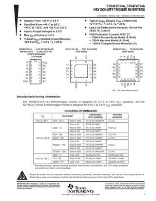
Original Logic IC SN74LVC14A SN54LVC14A 74LVC14A 54LVC14A SOP-14 New Texas Instruments
1. SN54LVC14A, SN74LVC14A
HEX SCHMITTĆTRIGGER INVERTERS
SCAS285W − MARCH 1993 − REVISED FEBRUARY 2004
1POST OFFICE BOX 655303 • DALLAS, TEXAS 75265
D Operate From 1.65 V to 3.6 V
D Specified From −40°C to 85°C,
−40°C to 125°C, and −55°C to 125°C
D Inputs Accept Voltages to 5.5 V
D Max tpd of 6.4 ns at 3.3 V
D Typical VOLP (Output Ground Bounce)
<0.8 V at VCC = 3.3 V, TA = 25°C
D Typical VOHV (Output VOH Undershoot)
>2 V at VCC = 3.3 V, TA = 25°C
D Latch-Up Performance Exceeds 100 mA Per
JESD 78, Class II
D ESD Protection Exceeds JESD 22
− 2000-V Human-Body Model (A114-A)
− 200-V Machine Model (A115-A)
− 1000-V Charged-Device Model (C101)
SN74LVC14A . . . RGY PACKAGE
(TOP VIEW)
1 14
7 8
2
3
4
5
6
13
12
11
10
9
6A
6Y
5A
5Y
4A
1Y
2A
2Y
3A
3Y
1A
4YV
GND
CC
1
2
3
4
5
6
7
14
13
12
11
10
9
8
1A
1Y
2A
2Y
3A
3Y
GND
VCC
6A
6Y
5A
5Y
4A
4Y
SN54LVC14A . . . J OR W PACKAGE
SN74LVC14A . . . D, DB, DGV, NS,
OR PW PACKAGE
(TOP VIEW)
3 2 1 20 19
9 10 11 12 13
4
5
6
7
8
18
17
16
15
14
6Y
NC
5A
NC
5Y
2A
NC
2Y
NC
3A
1Y
1A
NC
4Y
4A
V
6A
3Y
GND
NC
SN54LVC14A . . . FK PACKAGE
(TOP VIEW)
CC
NC − No internal connection
description/ordering information
The SN54LVC14A hex Schmitt-trigger inverter is designed for 2.7-V to 3.6-V VCC operation, and the
SN74LVC14A hex Schmitt-trigger inverter is designed for 1.65-V to 3.6-V VCC operation.
ORDERING INFORMATION
TA PACKAGE† ORDERABLE
PART NUMBER
TOP-SIDE
MARKING
−40°C to 85°C QFN − RGY Reel of 1000 SN74LVC14ARGYR LC14A
Tube of 50 SN74LVC14AD
SOIC − D Reel of 2500 SN74LVC14ADR LVC14ASOIC − D
Reel of 250 SN74LVC14ADT
LVC14A
SOP − NS Reel of 2000 SN74LVC14ANSR LVC14A
−40°C to 125°C SSOP − DB Reel of 2000 SN74LVC14ADBR LC14A−40 C to 125 C
Tube of 90 SN74LVC14APW
TSSOP − PW Reel of 2000 SN74LVC14APWR LC14ATSSOP − PW
Reel of 250 SN74LVC14APWT
LC14A
TVSOP − DGV Reel of 2000 SN74LVC14ADGVR LC14A
CDIP − J Tube of 25 SNJ54LVC14AJ SNJ54LVC14AJ
−55°C to 125°C CFP − W Tube of 150 SNJ54LVC14AW SNJ54LVC14AW−55 C to 125 C
LCCC − FK Tube of 55 SNJ54LVC14AFK SNJ54LVC14AFK
† Package drawings, standard packing quantities, thermal data, symbolization, and PCB design guidelines
are available at www.ti.com/sc/package.
Copyright 2004, Texas Instruments IncorporatedPRODUCTION DATA information is current as of publication date.
Products conform to specifications per the terms of Texas Instruments
standard warranty. Production processing does not necessarily include
testing of all parameters.
Please be aware that an important notice concerning availability, standard warranty, and use in critical applications of
Texas Instruments semiconductor products and disclaimers thereto appears at the end of this data sheet.
On products compliant to MILĆPRFĆ38535, all parameters are tested
unless otherwise noted. On all other products, production
processing does not necessarily include testing of all parameters.
2. SN54LVC14A, SN74LVC14A
HEX SCHMITTĆTRIGGER INVERTERS
SCAS285W − MARCH 1993 − REVISED FEBRUARY 2004
2 POST OFFICE BOX 655303 • DALLAS, TEXAS 75265
description/ordering information (continued)
The devices contain six independent inverters and perform the Boolean function Y = A.
Inputs can be driven from either 3.3-V or 5-V devices. This feature allows the use of these devices as translators
in a mixed 3.3-V/5-V system environment.
FUNCTION TABLE
(each inverter)
INPUT
A
OUTPUT
Y
H L
L H
logic diagram, each inverter (positive logic)
YA
absolute maximum ratings over operating free-air temperature range (unless otherwise noted)†
Supply voltage range, VCC −0.5 V to 6.5 V. . . . . . . . . . . . . . . . . . . . . . . . . . . . . . . . . . . . . . . . . . . . . . . . . . . . . . . . .
Input voltage range, VI (see Note 1) −0.5 V to 6.5 V. . . . . . . . . . . . . . . . . . . . . . . . . . . . . . . . . . . . . . . . . . . . . . . . .
Output voltage range, VO (see Notes 1 and 2) −0.5 V to VCC + 0.5 V. . . . . . . . . . . . . . . . . . . . . . . . . . . . . . . . . .
Input clamp current, IIK (VI < 0) −50 mA. . . . . . . . . . . . . . . . . . . . . . . . . . . . . . . . . . . . . . . . . . . . . . . . . . . . . . . . . . .
Output clamp current, IOK (VO < 0) −50 mA. . . . . . . . . . . . . . . . . . . . . . . . . . . . . . . . . . . . . . . . . . . . . . . . . . . . . . . .
Continuous output current, IO ±50 mA. . . . . . . . . . . . . . . . . . . . . . . . . . . . . . . . . . . . . . . . . . . . . . . . . . . . . . . . . . . . .
Continuous current through VCC or GND ±100 mA. . . . . . . . . . . . . . . . . . . . . . . . . . . . . . . . . . . . . . . . . . . . . . . . . .
Package thermal impedance, θJA (see Note 3): D package 86°C/W. . . . . . . . . . . . . . . . . . . . . . . . . . . . . . . . . . .
(see Note 3): DB package 96°C/W. . . . . . . . . . . . . . . . . . . . . . . . . . . . . . . . .
(see Note 3): DGV package 127°C/W. . . . . . . . . . . . . . . . . . . . . . . . . . . . . . .
(see Note 3): NS package 76°C/W. . . . . . . . . . . . . . . . . . . . . . . . . . . . . . . . .
(see Note 3): PW package 113°C/W. . . . . . . . . . . . . . . . . . . . . . . . . . . . . . . .
(see Note 4): RGY package 47°C/W. . . . . . . . . . . . . . . . . . . . . . . . . . . . . . . .
Storage temperature range, Tstg −65°C to 150°C. . . . . . . . . . . . . . . . . . . . . . . . . . . . . . . . . . . . . . . . . . . . . . . . . . .
Power dissipation, Ptot (TA = −40°C to 125°C) (see Notes 5 and 6) 500 mW. . . . . . . . . . . . . . . . . . . . . . . . . . . .
† Stresses beyond those listed under “absolute maximum ratings” may cause permanent damage to the device. These are stress ratings only, and
functional operation of the device at these or any other conditions beyond those indicated under “recommended operating conditions” is not
implied. Exposure to absolute-maximum-rated conditions for extended periods may affect device reliability.
NOTES: 1. The input negative-voltage and output voltage ratings may be exceeded if the input and output current ratings are observed.
2. The value of VCC is provided in the recommended operating conditions table.
3. The package thermal impedance is calculated in accordance with JESD 51-7.
4. The package thermal impedance is calculated in accordance with JESD 51-5.
5. For the D package: above 70°C, the value of Ptot derates linearly with 8 mW/K.
6. For the DB, DGV, NS, and PW packages: above 60°C, the value of Ptot derates linearly with 5.5 mW/K.
3. SN54LVC14A, SN74LVC14A
HEX SCHMITTĆTRIGGER INVERTERS
SCAS285W − MARCH 1993 − REVISED FEBRUARY 2004
3POST OFFICE BOX 655303 • DALLAS, TEXAS 75265
recommended operating conditions (see Note 7)
SN54LVC14A
−55 TO 125°C UNIT
MIN MAX
UNIT
VCC Supply voltage
Operating 2 3.6
VVCC Supply voltage
Data retention only 1.5
V
VI Input voltage 0 5.5 V
VO Output voltage 0 VCC V
IOH High-level output current
VCC = 2.7 V −12
mAIOH High-level output current
VCC = 3 V −24
mA
IOL Low-level output current
VCC = 2.7 V 12
mAIOL Low-level output current
VCC = 3 V 24
mA
NOTE 7: All unused inputs of the device must be held at VCC or GND to ensure proper device operation. Refer to the TI application report,
Implications of Slow or Floating CMOS Inputs, literature number SCBA004.
recommended operating conditions (see Note 7)
SN74LVC14A
TA = 25°C −40 TO 85°C −40 TO 125°C UNIT
MIN MAX MIN MAX MIN MAX
UNIT
VCC Supply voltage
Operating 1.65 3.6 1.65 3.6 1.65 3.6
VVCC Supply voltage
Data retention only 1.5 1.5 1.5
V
VI Input voltage 0 5.5 0 5.5 0 5.5 V
VO Output voltage 0 VCC 0 VCC 0 VCC V
VCC = 1.65 V −4 −4 −4
IOH High-level output current
VCC = 2.3 V −8 −8 −8
mAIOH High-level output current
VCC = 2.7 V −12 −12 −12
mA
VCC = 3 V −24 −24 −24
VCC = 1.65 V 4 4 4
IOL Low-level output current
VCC = 2.3 V 8 8 8
mAIOL Low-level output current
VCC = 2.7 V 12 12 12
mA
VCC = 3 V 24 24 24
NOTE 7: All unused inputs of the device must be held at VCC or GND to ensure proper device operation. Refer to the TI application report,
Implications of Slow or Floating CMOS Inputs, literature number SCBA004.
4. SN54LVC14A, SN74LVC14A
HEX SCHMITTĆTRIGGER INVERTERS
SCAS285W − MARCH 1993 − REVISED FEBRUARY 2004
4 POST OFFICE BOX 655303 • DALLAS, TEXAS 75265
electrical characteristics over recommended operating free-air temperature range (unless
otherwise noted)
SN54LVC14A
PARAMETER TEST CONDITIONS VCC −55 TO 125°C UNITPARAMETER TEST CONDITIONS VCC
MIN TYP MAX
UNIT
VT+
2.7 V 0.8 2VT+
Positive-going
threshold
3 V 0.9 2 VPositive-going
threshold 3.6 V 1.1 2
V
VT−
2.7 V 0.4 1.4VT−
Negative-going
threshold
3 V 0.6 1.5 VNegative-going
threshold 3.6 V 0.8 1.7
V
∆VT
2.7 V 0.3 1.1∆VT
Hysteresis
(V − V )
3 V 0.3 1.2 VHysteresis
(VT+ − VT−) 3.6 V 0.3 1.2
V
IOH = −100 µA 2.7 V to 3.6 V VCC−0.2
VOH IOH = −12 mA
2.7 V 2.2
VVOH IOH = −12 mA
3 V 2.4
V
IOH = −24 mA 3 V 2.2
IOL = 100 µA 2.7 V to 3.6 V 0.2
VOL IOL = 12 mA 2.7 V 0.4 VVOL
IOL = 24 mA 3 V 0.55
V
II VI = 5.5 V or GND 3.6 V ±5 µA
ICC VI = VCC or GND, IO = 0 3.6 V 10 µA
∆ICC One input at VCC − 0.6 V, Other inputs at VCC or GND 2.7 V to 3.6 V 500 µA
Ci VI = VCC or GND 3.3 V 5† pF
† TA = 25°C
5. SN54LVC14A, SN74LVC14A
HEX SCHMITTĆTRIGGER INVERTERS
SCAS285W − MARCH 1993 − REVISED FEBRUARY 2004
5POST OFFICE BOX 655303 • DALLAS, TEXAS 75265
electrical characteristics over recommended operating free-air temperature range (unless
otherwise noted)
SN74LVC14A
PARAMETER TEST CONDITIONS VCC TA = 25°C −40 TO 85°C −40 TO 125°C UNITPARAMETER TEST CONDITIONS VCC
MIN TYP MAX MIN MAX MIN MAX
UNIT
1.65 V 0.4 1.3 0.4 1.3 0.4 1.3
1.95 V 0.6 1.5 0.6 1.5 0.6 1.5
VT+
2.3 V 0.8 1.7 0.8 1.7 0.8 1.7VT+
Positive-going
threshold
2.5 V 0.8 1.7 0.8 1.7 0.8 1.7 VPositive-going
threshold 2.7 V 0.8 2 0.8 2 0.8 2
V
3 V 0.9 2 0.9 2 0.9 2
3.6 V 1.1 2 1.1 2 1.1 2
1.65 V 0.15 0.85 0.15 0.85 0.15 0.85
1.95 V 0.25 0.95 0.25 0.95 0.25 0.95
VT−
2.3 V 0.4 1.2 0.4 1.2 0.4 1.2VT−
Negative-going
threshold
2.5 V 0.4 1.2 0.4 1.2 0.4 1.2 VNegative-going
threshold 2.7 V 0.4 1.4 0.4 1.4 0.4 1.4
V
3 V 0.6 1.5 0.6 1.5 0.6 1.5
3.6 V 0.8 1.7 0.8 1.7 0.8 1.7
1.65 V 0.1 1.15 0.1 1.15 0.1 1.15
1.95 V 0.15 1.25 0.15 1.25 0.15 1.25
∆VT
2.3 V 0.25 1.3 0.25 1.3 0.25 1.3∆VT
Hysteresis
(V − V )
2.5 V 0.25 1.3 0.25 1.3 0.25 1.3 VHysteresis
(VT+ − VT−) 2.7 V 0.3 1.1 0.3 1.1 0.3 1.1
V
T+ T−
3 V 0.3 1.2 0.3 1.2 0.3 1.2
3.6 V 0.3 1.2 0.3 1.2 0.3 1.2
IOH = −100 µA 1.65 V to 3.6 V VCC−0.2 VCC−0.2 VCC−0.3
IOH = −4 mA 1.65 V 1.29 1.2 1.05
VOH
IOH = −8 mA 2.3 V 1.9 1.7 1.65
VVOH
IOH = −12 mA
2.7 V 2.2 2.2 2.05
V
IOH = −12 mA
3 V 2.4 2.4 2.25
IOH = −24 mA 3 V 2.3 2.2 2
IOL = 100 µA 1.65 V to 3.6 V 0.1 0.2 0.3
IOL = 4 mA 1.65 V 0.24 0.45 0.6
VOL IOL = 8 mA 2.3 V 0.3 0.7 0.75 VVOL
IOL = 12 mA 2.7 V 0.4 0.4 0.6
V
IOL = 24 mA 3 V 0.55 0.55 0.8
II VI = 5.5 V or GND 3.6 V ±1 ±5 ±20 µA
ICC VI = VCC or GND, IO = 0 3.6 V 1 10 40 µA
∆ICC
One input at
VCC − 0.6 V,
Other inputs at
VCC or GND
2.7 V to 3.6 V 500 500 5000 µA
Ci VI = VCC or GND 3.3 V 5 pF
6. SN54LVC14A, SN74LVC14A
HEX SCHMITTĆTRIGGER INVERTERS
SCAS285W − MARCH 1993 − REVISED FEBRUARY 2004
6 POST OFFICE BOX 655303 • DALLAS, TEXAS 75265
switching characteristics over recommended operating free-air temperature range (unless
otherwise noted) (see Figure 1)
FROM TO
SN54LVC14A
PARAMETER
FROM
(INPUT)
TO
(OUTPUT)
VCC −55 TO 125°C UNITPARAMETER
(INPUT) (OUTPUT)
VCC
MIN MAX
UNIT
tpd A Y
2.7 V 7.5
nstpd A Y
3.3 V ± 0.3 V 1 6.4
ns
switching characteristics over recommended operating free-air temperature range (unless
otherwise noted) (see Figure 1)
FROM TO
SN74LVC14A
PARAMETER
FROM
(INPUT)
TO
(OUTPUT)
VCC TA = 25°C −40 TO 85°C −40 TO 125°C UNITPARAMETER
(INPUT) (OUTPUT)
VCC
MIN TYP MAX MIN MAX MIN MAX
UNIT
1.8 V ± 0.15 V 1 5 10.5 1 11 1 13
tpd A Y
2.5 V ± 0.2 V 1 3.4 7.3 1 7.8 1 10
nstpd A Y
2.7 V 1 3.6 7.3 1 7.5 1 9.5
ns
3.3 V ± 0.3 V 1 3.2 6.2 1 6.4 1 8
tsk(o) 3.3 V ± 0.3 V 1 1 1.5 ns
operating characteristics, TA = 25°C
PARAMETER
TEST
CONDITIONS
VCC TYP UNIT
1.8 V 11
Cpd Power dissipation capacitance per inverter f = 10 MHz 2.5 V 12 pFCpd Power dissipation capacitance per inverter f = 10 MHz
3.3 V 15
pF
7. SN54LVC14A, SN74LVC14A
HEX SCHMITTĆTRIGGER INVERTERS
SCAS285W − MARCH 1993 − REVISED FEBRUARY 2004
7POST OFFICE BOX 655303 • DALLAS, TEXAS 75265
PARAMETER MEASUREMENT INFORMATION
VM
thtsu
From Output
Under Test
CL
(see Note A)
LOAD CIRCUIT
S1
VLOAD
Open
GND
RL
RL
Data Input
Timing Input
VI
0 V
VI
0 V0 V
tw
Input
VOLTAGE WAVEFORMS
SETUP AND HOLD TIMES
VOLTAGE WAVEFORMS
PROPAGATION DELAY TIMES
INVERTING AND NONINVERTING OUTPUTS
VOLTAGE WAVEFORMS
PULSE DURATION
tPLH
tPHL
tPHL
tPLH
VOH
VOH
VOL
VOL
VI
0 V
Input
Output
Waveform 1
S1 at VLOAD
(see Note B)
Output
Waveform 2
S1 at GND
(see Note B)
VOL
VOH
tPZL
tPZH
tPLZ
tPHZ
VLOAD/2
0 V
VOL + V∆
VOH − V∆
≈0 V
VI
VOLTAGE WAVEFORMS
ENABLE AND DISABLE TIMES
LOW- AND HIGH-LEVEL ENABLING
Output
Output
tPLH/tPHL
tPLZ/tPZL
tPHZ/tPZH
Open
VLOAD
GND
TEST S1
NOTES: A. CL includes probe and jig capacitance.
B. Waveform 1 is for an output with internal conditions such that the output is low, except when disabled by the output control.
Waveform 2 is for an output with internal conditions such that the output is high, except when disabled by the output control.
C. All input pulses are supplied by generators having the following characteristics: PRR ≤ 10 MHz, ZO = 50 Ω.
D. The outputs are measured one at a time, with one transition per measurement.
E. tPLZ and tPHZ are the same as tdis.
F. tPZL and tPZH are the same as ten.
G. tPLH and tPHL are the same as tpd.
H. All parameters and waveforms are not applicable to all devices.
Output
Control
VM VM
VM VM
VM VM
VM
VM VM
VM
VM
VM
VI
VM
VM
1.8 V ± 0.15 V
2.5 V ± 0.2 V
2.7 V
3.3 V ± 0.3 V
1 kΩ
500 Ω
500 Ω
500 Ω
VCC RL
2 × VCC
2 × VCC
6 V
6 V
VLOAD CL
30 pF
30 pF
50 pF
50 pF
0.15 V
0.15 V
0.3 V
0.3 V
V∆
VCC
VCC
2.7 V
2.7 V
VI
VCC/2
VCC/2
1.5 V
1.5 V
VMtr/tf
≤2 ns
≤2 ns
≤2.5 ns
≤2.5 ns
INPUTS
Figure 1. Load Circuit and Voltage Waveforms
8.
9. MECHANICAL DATA
MCFP002A – JANUARY 1995 – REVISED FEBRUARY 2002
POST OFFICE BOX 655303 • DALLAS, TEXAS 75265
W (R-GDFP-F14) CERAMIC DUAL FLATPACK
0.360 (9,14)
0.250 (6,35)
87
141
0.235 (5,97)
0.004 (0,10)
0.026 (0,66)
4 Places
0.015 (0,38)
0.045 (1,14)
0.335 (8,51)
0.008 (0,20)
0.045 (1,14)
Base and Seating Plane
0.005 (0,13) MIN
0.019 (0,48)
0.390 (9,91)
0.260 (6,60)
0.080 (2,03)
4040180-2/C 02/02
0.360 (9,14)
0.250 (6,35)
0.280 (7,11) MAX
0.050 (1,27)
NOTES: A. All linear dimensions are in inches (millimeters).
B. This drawing is subject to change without notice.
C. This package can be hermetically sealed with a ceramic lid using glass frit.
D. Index point is provided on cap for terminal identification only.
E. Falls within MIL STD 1835 GDFP1-F14 and JEDEC MO-092AB
10. MECHANICAL DATA
MLCC006B – OCTOBER 1996
POST OFFICE BOX 655303 • DALLAS, TEXAS 75265
FK (S-CQCC-N**) LEADLESS CERAMIC CHIP CARRIER
4040140/D 10/96
28 TERMINAL SHOWN
B
0.358
(9,09)
MAX
(11,63)
0.560
(14,22)
0.560
0.458
0.858
(21,8)
1.063
(27,0)
(14,22)
ANO. OF
MINMAX
0.358
0.660
0.761
0.458
0.342
(8,69)
MIN
(11,23)
(16,26)
0.640
0.739
0.442
(9,09)
(11,63)
(16,76)
0.962
1.165
(23,83)
0.938
(28,99)
1.141
(24,43)
(29,59)
(19,32)(18,78)
**
20
28
52
44
68
84
0.020 (0,51)
TERMINALS
0.080 (2,03)
0.064 (1,63)
(7,80)
0.307
(10,31)
0.406
(12,58)
0.495
(12,58)
0.495
(21,6)
0.850
(26,6)
1.047
0.045 (1,14)
0.045 (1,14)
0.035 (0,89)
0.035 (0,89)
0.010 (0,25)
121314151618 17
11
10
8
9
7
5
432
0.020 (0,51)
0.010 (0,25)
6
12826 27
19
21
B SQ
A SQ
22
23
24
25
20
0.055 (1,40)
0.045 (1,14)
0.028 (0,71)
0.022 (0,54)
0.050 (1,27)
NOTES: A. All linear dimensions are in inches (millimeters).
B. This drawing is subject to change without notice.
C. This package can be hermetically sealed with a metal lid.
D. The terminals are gold plated.
E. Falls within JEDEC MS-004
11. MECHANICAL DATA
MPDS006C – FEBRUARY 1996 – REVISED AUGUST 2000
POST OFFICE BOX 655303 • DALLAS, TEXAS 75265
DGV (R-PDSO-G**) PLASTIC SMALL-OUTLINE
24 PINS SHOWN
14
3,70
3,50 4,90
5,10
20
DIM
PINS **
4073251/E 08/00
1,20 MAX
Seating Plane
0,05
0,15
0,25
0,50
0,75
0,23
0,13
1 12
24 13
4,30
4,50
0,16 NOM
Gage Plane
A
7,90
7,70
382416
4,90
5,103,70
3,50
A MAX
A MIN
6,60
6,20
11,20
11,40
56
9,60
9,80
48
0,08
M0,070,40
0°–ā8°
NOTES: A. All linear dimensions are in millimeters.
B. This drawing is subject to change without notice.
C. Body dimensions do not include mold flash or protrusion, not to exceed 0,15 per side.
D. Falls within JEDEC: 24/48 Pins – MO-153
14/16/20/56 Pins – MO-194
12.
13.
14.
15. MECHANICAL DATA
MSSO002E – JANUARY 1995 – REVISED DECEMBER 2001
POST OFFICE BOX 655303 • DALLAS, TEXAS 75265
DB (R-PDSO-G**) PLASTIC SMALL-OUTLINE
4040065 /E 12/01
28 PINS SHOWN
Gage Plane
8,20
7,40
0,55
0,95
0,25
38
12,90
12,30
28
10,50
24
8,50
Seating Plane
9,907,90
30
10,50
9,90
0,38
5,60
5,00
15
0,22
14
A
28
1
2016
6,506,50
14
0,05 MIN
5,905,90
DIM
A MAX
A MIN
PINS **
2,00 MAX
6,90
7,50
0,65 M0,15
0°–ā8°
0,10
0,09
0,25
NOTES: A. All linear dimensions are in millimeters.
B. This drawing is subject to change without notice.
C. Body dimensions do not include mold flash or protrusion not to exceed 0,15.
D. Falls within JEDEC MO-150
16. MECHANICAL DATA
MTSS001C – JANUARY 1995 – REVISED FEBRUARY 1999
POST OFFICE BOX 655303 • DALLAS, TEXAS 75265
PW (R-PDSO-G**) PLASTIC SMALL-OUTLINE PACKAGE
14 PINS SHOWN
0,65 M0,10
0,10
0,25
0,50
0,75
0,15 NOM
Gage Plane
28
9,80
9,60
24
7,90
7,70
2016
6,60
6,40
4040064/F 01/97
0,30
6,60
6,20
8
0,19
4,30
4,50
7
0,15
14
A
1
1,20 MAX
14
5,10
4,90
8
3,10
2,90
A MAX
A MIN
DIM
PINS **
0,05
4,90
5,10
Seating Plane
0°–8°
NOTES: A. All linear dimensions are in millimeters.
B. This drawing is subject to change without notice.
C. Body dimensions do not include mold flash or protrusion not to exceed 0,15.
D. Falls within JEDEC MO-153
17. IMPORTANT NOTICE
Texas Instruments Incorporated and its subsidiaries (TI) reserve the right to make corrections, modifications,
enhancements, improvements, and other changes to its products and services at any time and to discontinue
any product or service without notice. Customers should obtain the latest relevant information before placing
orders and should verify that such information is current and complete. All products are sold subject to TI’s terms
and conditions of sale supplied at the time of order acknowledgment.
TI warrants performance of its hardware products to the specifications applicable at the time of sale in
accordance with TI’s standard warranty. Testing and other quality control techniques are used to the extent TI
deems necessary to support this warranty. Except where mandated by government requirements, testing of all
parameters of each product is not necessarily performed.
TI assumes no liability for applications assistance or customer product design. Customers are responsible for
their products and applications using TI components. To minimize the risks associated with customer products
and applications, customers should provide adequate design and operating safeguards.
TI does not warrant or represent that any license, either express or implied, is granted under any TI patent right,
copyright, mask work right, or other TI intellectual property right relating to any combination, machine, or process
in which TI products or services are used. Information published by TI regarding third-party products or services
does not constitute a license from TI to use such products or services or a warranty or endorsement thereof.
Use of such information may require a license from a third party under the patents or other intellectual property
of the third party, or a license from TI under the patents or other intellectual property of TI.
Reproduction of information in TI data books or data sheets is permissible only if reproduction is without
alteration and is accompanied by all associated warranties, conditions, limitations, and notices. Reproduction
of this information with alteration is an unfair and deceptive business practice. TI is not responsible or liable for
such altered documentation.
Resale of TI products or services with statements different from or beyond the parameters stated by TI for that
product or service voids all express and any implied warranties for the associated TI product or service and
is an unfair and deceptive business practice. TI is not responsible or liable for any such statements.
Following are URLs where you can obtain information on other Texas Instruments products and application
solutions:
Products Applications
Amplifiers amplifier.ti.com Audio www.ti.com/audio
Data Converters dataconverter.ti.com Automotive www.ti.com/automotive
DSP dsp.ti.com Broadband www.ti.com/broadband
Interface interface.ti.com Digital Control www.ti.com/digitalcontrol
Logic logic.ti.com Military www.ti.com/military
Power Mgmt power.ti.com Optical Networking www.ti.com/opticalnetwork
Microcontrollers microcontroller.ti.com Security www.ti.com/security
Telephony www.ti.com/telephony
Video & Imaging www.ti.com/video
Wireless www.ti.com/wireless
Mailing Address: Texas Instruments
Post Office Box 655303 Dallas, Texas 75265
Copyright 2004, Texas Instruments Incorporated