SlideShare a Scribd company logo
1 of 36
Download to read offline
UCC28060
1NATURAL INTERLEAVING FEATURES SYSTEM FEATURES
APPLICATIONS
+–
COMP
VREF
PGNDAGND
VCC ZCDA
ZCDB
GDA
CS
GDB
VINAC
VSENSE
PWMCNTL
UCC28061
TSET
PHB
HVSEN
EMI
Filter
400 VDC
Power Good to
downstream converter
85-265VAC
Input Voltage (V)
5
4
3
2
1
70 120 170 220 270
CapacitorRippleCurrent(A)
P = 600 W
V = 400 V
OUT
OUT
1-Phase TM
2-Phase TM Interleave
1-Phase CCM
UCC28061
www.ti.com .............................................................................................................................................................. SLUS837A–JUNE 2008–REVISED JULY 2009
Natural Interleaving™ Transition-Mode PFC Controller With Improved Audible Noise
Immunity
• Improved Audible Noise Performance23• Phase Management Capability
• Soft Start on Overvoltage• FailSafe OVP with Dual Paths Prevents Output
• Integrated BrownoutOver-Voltage Conditions Caused by
Voltage-Sensing Failures • Improved Efficiency and Design Flexibility
over Traditional, Single-Phase Continuous• Sensorless Current Shaping Simplifies Board
Conduction Mode (CCM)Layout and Improves Efficiency
• Input Filter and Output Capacitor Current• Inrush Safe Current Limiting:
Cancellation:
– Prevents MOSFET conduction during
– Reduced current ripple for higher system
inrush reliability and smaller bulk capacitor
– Eliminates reverse recovery events in – Reduced EMI filter size
output rectifiers • Enables Use of Low-Cost Diodes without
Extensive Snubber Circuitry
• Improved Light-Load Efficiency
• Improved Transient Response
• Complete System-Level Protection
• 1-A Source/1.8-A Sink Gate Drivers
• 100-W to 800-W Power Supplies
• Gaming
• D to A Set Top Boxes
• Adapters
• LCD, Plasma and DLP™ TVs
• Home Audio Systems
Typical Application Circuit
Ripple Current Reduction
1
Please be aware that an important notice concerning availability, standard warranty, and use in critical applications of Texas
Instruments semiconductor products and disclaimers thereto appears at the end of this data sheet.
2DLP is a trademark of Texas Instruments.
3Natural Interleaving is a trademark of Texas Instuments.
PRODUCTION DATA information is current as of publication date. Copyright © 2008–2009, Texas Instruments Incorporated
Products conform to specifications per the terms of the Texas
Instruments standard warranty. Production processing does not
necessarily include testing of all parameters.
CONTENTS
DESCRIPTION
UCC28061
SLUS837A–JUNE 2008–REVISED JULY 2009 .............................................................................................................................................................. www.ti.com
• Ordering Information 2
• Electrical Characteristics 4
• Device Information 7
• Functional Block Diagram 9
• Typical Characteristics 10
• Application Information 16
• Design Example 22
• Additional References 29
Optimized for consumer applications concerned with audible noise elimination, this solution extends the
advantages of transition mode—high efficiency with low-cost components—to higher power ratings than
previously possible. By utilizing a Natural Interleaving technique, both channels operate as masters (that is, there
is no slave channel) synchronized to the same frequency. This approach delivers inherently strong matching,
faster responses, and ensures that each channel operates in transition mode.
Complete system-level protections feature input brownout, output over-voltage, open-loop, overload, soft-start,
phase-fail detection, and thermal shutdown. The additional FailSafe over-voltage protection (OVP) feature
protects against shorts to an intermediate voltage that, if undetected, could lead to catastrophic device failure.
This integrated circuit can be damaged by ESD. Texas Instruments recommends that all integrated circuits be handled with
appropriate precautions. Failure to observe proper handling and installation procedures can cause damage.
ESD damage can range from subtle performance degradation to complete device failure. Precision integrated circuits may be more
susceptible to damage because very small parametric changes could cause the device not to meet its published specifications.
ORDERING INFORMATION(1)
PART NUMBER PACKAGE(2)
OPERATING TEMPERATURE RANGE, TA
UCC28061D SOIC 16-Pin (D) –40°C to +125°C
(1) For the most current package and ordering information see the Package Option Addendum at the end of this document, or see the TI
web site at www.ti.com.
(2) SOIC (D) package is available taped and reeled by adding R to the above part number. Reeled quantities for UCC28061DR are 2500
devices per reel.
2 Submit Documentation Feedback Copyright © 2008–2009, Texas Instruments Incorporated
Product Folder Link(s): UCC28061
ABSOLUTE MAXIMUM RATINGS(1)
DISSIPATION RATINGS
RECOMMENDED OPERATING CONDITIONS
ELECTROSTATIC DISCHARGE (ESD) PROTECTION
UCC28061
www.ti.com .............................................................................................................................................................. SLUS837A–JUNE 2008–REVISED JULY 2009
All voltages are with respect to GND, –40°C < TJ = TA < +125°C, and currents are positive into and negative out of the
specified terminal, unless otherwise noted.
UCC28061 UNIT
VCC(2)
–0.5 to +21
PWMCNTL –0.5 to +20
Input voltage range V
COMP(3)
, CS, PHB, HVSEN(4)
, VINAC(4)
, VSENSE(4)
–0.5 to +7
ZCDA, ZCDB –0.5 to +4
Continuous input current VCC 20
Input current PWMCNTL 10
Input current range ZCDA, ZCDB, VSENSE –5 to +5 mA
Output current VREF –10
Continuous gate current GDA, GDB(5)
±25
Operating –40 to +125
Junction temperature, TJ
Storage –65 to +150 °C
Lead temperature, TSOL Soldering, 10s +260
(1) Stresses beyond those listed under absolute maximum ratings may cause permanent damage to the device. These are stress ratings
only and functional operation of the device at these or any other condition beyond those included under recommended operating
conditions is not implied. Exposure to absolute-maximum-rated conditions for extended periods of time may affect device reliability.
(2) Voltage on VCC is internally clamped. VCC may exceed the absolute maximum input voltage if the source is current limited below the
absolute maximum continuous VCC input current level.
(3) In normal use, COMP is connected to capacitors and resistors and is internally limited in voltage swing.
(4) In normal use, VINAC, VSENSE, and HVSEN are connected to resistors and are internally limited in voltage swing. Although not
recommended for extended use, VINAC, VSENSE, and HVSEN can survive input currents as high as ±10 mA from high voltage
sources.
(5) No GDA or GDB current limiting is required when driving a power MOSFET gate. However, a small series resistor may be required to
damp ringing due to stray inductance. See Figure 12 and Figure 13 for details.
THERMAL IMPEDANCE
PACKAGE JUNCTION-TO-AMBIENT TA = +25°C POWER RATING TA = +85°C POWER RATING
SOIC 16-Pin (D) 140°C/W(1)
890 mW(1)
460 mW(1)
(1) Tested per JEDEC EIA/JESD 51-1. Thermal resistance is a strong function of board construction and layout. Air flow will reduce thermal
resistance. This number is only a general guide; see TI document SPRA953 device Thermal Metrics.
All voltages are with respect to GND, –40°C < TJ = TA < +125°C, and currents are positive into and negative out of the
specified terminal, unless otherwise noted.
MIN MAX UNIT
VCC input voltage from a low-impedance source 14 21 V
VCC input current from a high-impedance source 8 18
mA
VREF load current 0 –2
VINAC Input voltage 0 6 V
ZCDA, ZCDB series resistor 20 80
kΩ
TSET resistor to program PWM on-time 66.5 400
HVSEN input voltage 0.8 4.5 V
PWMCNTL pull-up resistor to VREF 1 10 kΩ
RATING UNIT
Human body model (HBM) 2000 V
Charged device model (CDM) 500 V
Copyright © 2008–2009, Texas Instruments Incorporated Submit Documentation Feedback 3
Product Folder Link(s): UCC28061
ELECTRICAL CHARACTERISTICS
UCC28061
SLUS837A–JUNE 2008–REVISED JULY 2009 .............................................................................................................................................................. www.ti.com
At VCC = 16 V, AGND = PGND = 0 V, VINAC = 3 V, VSENSE = 6 V, HVSEN = 3 V, PHB = 5 V, RTSET = 133 kΩ; all voltages
are with respect to GND, all outputs unloaded, –40°C < TJ = TA < +125°C, and currents are positive into and negative out of
the specified terminal, unless otherwise noted.
PARAMETER TEST CONDITIONS MIN TYP MAX UNIT
VCC BIAS SUPPLY
VCC(shunt) VCC shunt voltage(1)
IVCC = 10 mA 22 24 26 V
IVCC(stby) VCC current, disabled VSENSE = 0 V 100 200 µA
IVCC(on) VCC current, enabled VSENSE = 6 V 5 8 mA
UNDERVOLTAGE LOCKOUT (UVLO)
VCC(on) VCC turn-on threshold 11.5 12.6 13.5
VCC(off) VCC turn-off threshold 9.5 10.35 11.5 V
UVLO Hysteresis 1.85 2.25 2.65
REFERENCE
VREF VREF output voltage, no load IVREF = 0 mA 5.82 6.00 6.18 V
VREF change with load 0 mA ≤ IVREF ≤ –2 mA 1 6
mV
VREF change with VCC 12 V ≤ VCC ≤ 20 V 1 10
ERROR AMPLIFIER
VSENSE input regulation voltage TA = +25°C 5.85 6.00 6.15
V
VSENSE input regulation voltage 5.82 6.00 6.18
VSENSE input bias current In regulation 125 300 800 nA
COMP high voltage, clamped VSENSE = 5.8 V 4.70 4.95 5.10
V
COMP low voltage, saturated VSENSE = 6.2 V 0.03 0.125
COMP = 3 V,
gm VSENSE to COMP transconductance 75 96 110 µS
5.94 V < VSENSE < 6.06 V
COMP source current, overdriven VSENSE = 5 V, COMP = 3 V –120 –160 –190
µA
COMP sink current VSENSE = 6.2 V, COMP = 3 V 7 20 32
VSENSE threshold for COMP offset enable, down
Voltage below VREF 135 185 235 mV
from VREF
VOVP VSENSE over-voltage threshold, rising 6.25 6.45 6.7
VSENSE over-voltage hysteresis 0.1 0.2 0.4
V
VSENSE enable threshold, rising 1.15 1.25 1.35
VSENSE enable hysteresis 0.02 0.05 0.2
OUTPUT MONITORING
VPWMCNTL HVSEN threshold to PWMCNTL HVSEN rising 2.35 2.50 2.65 V
HVSEN input bias current, high HVSEN = 3 V –0.5 0.5
µA
HVSEN input bias current, low HVSEN = 2 V 28 36 41
HVSEN rising threshold to over-voltage fault 4.64 4.87 5.1
V
HVSEN falling threshold to over-voltage fault 4.45 4.67 4.80
PHB = 5 V,
Phase Fail filter time to PWMCNTL high 8 12 20 ms
ZCDA switching, ZCDB = 0.5 V
PWMCNTL leakage current high HVSEN = 2 V, PWMCNTL = 15 V –1 1 µA
PWMCNTL output voltage low HVSENS = 3 V, IPWMCNTL = 5 mA 0.2 0.5 V
(1) Excessive VCC input voltage and current will damage the device. This clamp does not protect the device from an unregulated supply. If
an unregulated supply is used, a Fixed Positive Voltage Regulator such as the UA78L15A is recommended. See the Absolute Maximum
Ratings table for the limits on VCC voltage and current.
4 Submit Documentation Feedback Copyright © 2008–2009, Texas Instruments Incorporated
Product Folder Link(s): UCC28061
UCC28061
www.ti.com .............................................................................................................................................................. SLUS837A–JUNE 2008–REVISED JULY 2009
ELECTRICAL CHARACTERISTICS (continued)
At VCC = 16 V, AGND = PGND = 0 V, VINAC = 3 V, VSENSE = 6 V, HVSEN = 3 V, PHB = 5 V, RTSET = 133 kΩ; all voltages
are with respect to GND, all outputs unloaded, –40°C < TJ = TA < +125°C, and currents are positive into and negative out of
the specified terminal, unless otherwise noted.
PARAMETER TEST CONDITIONS MIN TYP MAX UNIT
GATE DRIVE(2)
GDA, GDB output voltage high IGDA, IGDB = –100 mA 11.5 13 15
GDA, GDB output voltage high, clamped VCC = 20 V, IGDA, IGDB = –5 mA 12 13.5 15 V
GDA, GDB output voltage high, low VCC VCC = 12 V, IGDA, IGDB = –5 mA 10 10.5 11.5
GDA, GDB on-resistance high IGDA, IGDB = –100 mA 8 14 Ω
GDA, GDB output voltage low IGDA, IGDB = 100 mA 0.15 0.3 V
GDA, GDB on-resistance low IGDA, IGDB = 100 mA 2 3 Ω
Rise time 1 V to 9 V, CLOAD = 1 nF 18 30
ns
Fall time 9 V to 1 V, CLOAD = 1 nF 12 25
GDA, GDB output voltage UV IGDA, IGDB = 2.5 mA 1.6 2 V
ZERO CURRENT DETECTOR
ZCDA, ZCDB voltage threshold, falling 0.8 1.0 1.2
ZCDA, ZCDB voltage threshold, rising 1.5 1.68 1.88 V
ZCDA, ZCDB clamp, high IZCDA = +2 mA, IZCDB = +2 mA 2.6 3.0 3.4
ZCDA, ZCDB input bias current ZCDA = 1.4 V, ZCDB = 1.4 V –0.5 0.5 µA
ZCDA, ZCDB clamp, low IZCDA = –2 mA, IZCDB = –2 mA –0.4 –0.2 0 V
Respective gate drive output rising 10%
ZCDA, ZCDB delay to GDA, GDB outputs(2)
45 100 ns
from zero crossing input falling to 1 V
CURRENT SENSE
CS input bias current At rising threshold –150 –250 µA
CS current limit rising threshold –0.18 –0.20 –0.22
V
CS current limit falling threshold –0.005 –0.015 –0.029
From CS exceeding threshold –0.05 V to
CS current limit response time(2)
60 100 ns
GDx dropping 10%
MAINS INPUT
VINAC input bias current VINAC = 2 V –0.5 0.5 µA
BROWNOUT
VINAC brownout threshold VINAC falling 1.34 1.39 1.44 V
VINAC brownout current VINAC = 1 V 5 7 9 µA
VINAC fails to exceed the brownout
VINAC brownout filter time 340 440 540 ms
threshold for the brownout filter time
(2) Refer to Figure 12, Figure 13, Figure 14, and Figure 15 in the Typical Characteristics for typical gate drive waveforms.
Copyright © 2008–2009, Texas Instruments Incorporated Submit Documentation Feedback 5
Product Folder Link(s): UCC28061
UCC28061
SLUS837A–JUNE 2008–REVISED JULY 2009 .............................................................................................................................................................. www.ti.com
ELECTRICAL CHARACTERISTICS (continued)
At VCC = 16 V, AGND = PGND = 0 V, VINAC = 3 V, VSENSE = 6 V, HVSEN = 3 V, PHB = 5 V, RTSET = 133 kΩ; all voltages
are with respect to GND, all outputs unloaded, –40°C < TJ = TA < +125°C, and currents are positive into and negative out of
the specified terminal, unless otherwise noted.
PARAMETER TEST CONDITIONS MIN TYP MAX UNIT
PULSE-WIDTH MODULATOR
KTL On-time factor, phases A and B VINAC = 3.2 V, VSENSE = 5.8 V(3)
3.6 4.0 4.4
µs/VVINAC = 3.2 V, VSENSE = 5.8 V,
KTLS On-time factor, single-phase, A 7.2 8 8.9
PHB = 0 V(3)
Phase B to phase A on-time matching VSENSE = 5.8 V, VINAC = 3.2 V –6% 6%
COMP = 0.25 V, VINAC = 1 V 1.2 2 2.7Zero-crossing distortion correction additional on
µs
time COMP = 0.25 V, VINAC = 0.1 V 12.6 20 29
PHB threshold falling, to single-phase operation To GDB output shutdown VINAC = 1.5 V 0.7 0.8 0.9
V
PHB threshold rising, to two-phase operation To GDB output running VINAC = 1.5 V 0.9 1.0 1.1
T(min) Minimum switching period RTSET = 133 kΩ(3)
1.7 2.2 2.5
µs
PWM restart time ZCDA = ZCDB = 2 V(4)
165 200 265
THERMAL SHUTDOWN
Thermal shutdown temperature TJ, temperature rising(5)
+160
°C
Thermal restart temperature TJ, temperature falling(5)
+140
(3) Gate drive on-time is proportional to VCOMP – 125 mV. The on-time proportionality factor, KT, is different in two-phase and single-phase
modes. The on-time factor, KT, scales linearly with the value of RTSET. The minimum switching period is proportional to RTSET.
(4) An output on-time is generated at both GDA and GDB if both ZCDA and ZCDB negative-going edges are not detected for the restart
time. In single-phase mode, the restart time applies for the ZCDA input and the GDA output.
(5) Thermal shutdown occurs at temperatures higher than the normal operating range. Device performance above the normal operating
temperature is not specified or assured.
6 Submit Documentation Feedback Copyright © 2008–2009, Texas Instruments Incorporated
Product Folder Link(s): UCC28061
DEVICE INFORMATION
ZCDA
VREF
GDA
PGND
VCC
GDB
CS
PWMCNTL
ZCDB
VSENSE
TSET
PHB
COMP
AGND
VINAC
HVSEN
1
2
3
4
5
6
7
8
16
15
14
13
12
11
10
9
UCC28061
www.ti.com .............................................................................................................................................................. SLUS837A–JUNE 2008–REVISED JULY 2009
UCC28061D
SOIC 16-Pin (D)
Top View
TERMINAL FUNCTIONS
TERMINAL
DESCRIPTION
NAME NO. I/O
Analog ground: Connect analog signal bypass capacitors, compensation components, and analog
AGND 6 — signal returns to this pin. Connect the analog and power grounds at a single point to isolate high-current
noise signals of the power components from interference with the low-current analog circuits.
Error amplifier output: The error amplifier is a transconductance amplifier, so this output is a
high-impedance current source. Connect voltage regulation loop compensation components from this
pin to AGND. The on-time seen at the gate drive outputs is proportional to the voltage at this pin minus
an offset of approximately 125 mV. During soft-start events (undervoltage, brownout, disable or output
COMP 5 O
over voltage), COMP is pulled low. Normal operation only resumes after the soft-start event clears and
COMP has been discharged below 0.5 V, making sure that the circuit restarts with a low COMP voltage
and a short on-time. Do not connect COMP to a low-impedance source that would interfere with COMP
falling below 0.5 V.
Current sense input: Connect the current sense resistor and the negative terminal of the diode bridge
to this pin. Connect the return of the current sense resistor to the AGND pin with a separate trace. As
input current increases, the voltage on CS goes more negative. This cycle-by-cycle over-current
protection limits input current by turning off both gate driver (GDx) outputs when CS is more negative
than the CS rising threshold (approximately –200 mV). The GD outputs remain low until CS falls to the
CS 10 I CS falling threshold (approximately –15 mV). Current sense is blanked for approximately 100 ns
following the falling edge of either GD output. This blanking filters noise that occurs when current
switches from a power FET to a boost diode. In most cases, no additional current sense filtering is
required. If filtering is required, the filter series resistance must be under 100 Ω to maintain accuracy. To
prevent excessive negative voltage on the CS pin during inrush conditions, connect the current sensing
resistor to the CS pin through a low value external resistor.
GDA 14 O Channel A and channel B gate drive output: Connect these pins to the gate of the power FET for
each phase through the shortest connection practical. If it is necessary to use a trace longer than 0.5
inch (12.6 mm) for this connection, some ringing may occur due to trace series inductance. This ringingGDB 11 O
can be reduced by adding a 5-Ω to 10-Ω resistor in series with GDA and GDB.
High voltage output sense: The UCC28061 incorporates FailSafe OVP so that any single failure does
not allow the output to boost above safe levels. Output over-voltage is monitored by both VSENSE and
HVSEN and shuts down the PWM if either pin exceeds the appropriate over-voltage threshold. Using
two pins to monitor for over-voltage provides redundant protection and fault tolerance. HVSEN can also
be used to enable a downstream power converter when the voltage on HVSEN is within the operating
HVSEN 8 I
region. Select the HVSEN divider ratio for the desired over-voltage and power-good thresholds. Select
the HVSEN divider impedance for the desired power-good hysteresis. During operation, HVSEN must
never fall below 0.8 V. Dropping HVSEN below 0.8 V puts the UCC28061 into a special test mode, used
only for factory testing. A bypass capacitor from HVSEN to AGND is recommended to filter noise and
prevent false over-voltage shutdown.
Power ground for the integrated circuit: Connect this pin to AGND through a separate short trace to
PGND 13 —
isolate gate driver noise from analog signals.
Phase B enable: This pin turns on/off channel B of the boost converter. The commanded on-time for
channel A is immediately doubled when channel B is disabled, which helps to keep COMP voltage
PHB 4 I constant during the phase management transient. The PHB pin allows the user to add external phase
management circuitry if they desire. To disable phase management, connect the PHB pin to the VREF
pin.
Copyright © 2008–2009, Texas Instruments Incorporated Submit Documentation Feedback 7
Product Folder Link(s): UCC28061
UCC28061
SLUS837A–JUNE 2008–REVISED JULY 2009 .............................................................................................................................................................. www.ti.com
TERMINAL FUNCTIONS (continued)
TERMINAL
DESCRIPTION
NAME NO. I/O
PWM enable logic output: This open-drain output goes low when HVSEN is within the HVSEN good
PWMCNTL 9 O region and the ZCDA and ZCDB inputs are switching correctly if operating in two-phase mode (see PHB
Pin). Otherwise, PWMCNTL is high impedance.
Timing set: PWM on-time programming input. Connect a resistor from TSET to AGND to set the
TSET 3 I
on-time versus COMP voltage and the minimum period at the gate drive outputs.
Bias supply input: Connect this pin to a controlled bias supply of between 14 V and 21 V. Also connect
a 0.1-µF ceramic bypass capacitor from this pin to PGND with the shortest possible board trace. This
VCC 12 —
supply powers all circuits in the device and must be capable of delivering 6 mA dc plus the transient
power MOSFET gate charging current.
Input ac voltage sense: For normal operation, connect this pin to a voltage divider across the rectified
input power mains. When the voltage on VINAC remains below the brownout threshold for more than
VINAC 7 I the brownout filter time, the device enters a brownout mode and both output drives are disabled. Select
the input voltage divider ratio for the desired brownout threshold. Select the divider impedance for the
desired brownout hysteresis.
Voltage reference output: Connect a 0.1-µF ceramic bypass capacitor from this pin to AGND. VREF
VREF 15 O turns off during VCC undervoltage and VSENSE disable to save supply current and increase efficiency.
This 6 VDC reference can be used to bias other circuits requiring less than 2 mA of total supply current.
Output dc voltage sense: Connect this pin to a voltage divider across the output of the power
converter. The error amplifier reference voltage is 6 V. Select the output voltage divider ratio for the
desired output voltage. Connect the ground side of this divider to ground through a separate short trace
VSENSE 2 I for best output regulation accuracy and noise immunity. VSENSE can be pulled low by an open-drain
logic output or 6-V logic output in series with a low-leakage diode to disable the outputs and reduce
VCC current. If VSENSE is disconnected, open-loop protection provides an internal current source to
pull VSENSE low, turning off the gate drivers.
Zero current detection inputs: These inputs expect to see a negative edge when the inductor current
in the respective phases go to zero. The inputs are clamped at 0 V and 3 V. Signals should be coupled
ZCDA 16 I
through a series resistor that limits the clamping current to less than ±3 mA. Connect these pins through
a current limiting resistor to the zero crossing detection windings of the appropriate boost
inductor. The inductor winding must be connected so that this voltage drops when inductor current
decays to zero. When the inductor current drops to zero, the ZCD input must drop below the falling
ZCDB 1 I threshold, approximately 1 V, to cause the gate drive output to rise. When the power MOSFET turns off,
the ZCD input must rise above the rising threshold, approximately 1.7 V, to arm the logic for another
falling ZCD edge.
8 Submit Documentation Feedback Copyright © 2008–2009, Texas Instruments Incorporated
Product Folder Link(s): UCC28061
7VINAC
+1.4V
Brownout440ms Delay
7mA
Crossover
Notch
Reduction
Phase A
On Time Control
3
1.68V/1V
ZCDA
+
1.68V/1V
ZCDB
+
16
1
Phase B
On Time Control
2VSENSE
+
VREF
gm
6V15
EN
+
6.45V
OV
+
4.95V
300nA
TSET
STOPA
STOPB
5
COMP
222mV
Brownout
EN
UV
+
12 VCC
GDA
13 PGND
UV
12.6V
10.35V
24V
11 GDB
14
+
13.5V
PGND
Interleave
Control
4.87V
9
PWMCNTL
36mA
8 HVSEN
Phase
OK
2.5V
+
+
HVSEN OV
10CS
Overcurrent
+
OV
OC
TSD
STOPA
HVSENOV
Burst Operation
STOPB
SinglePhase
-0.2V/-0.015V
OC
+0.8V
Single
Phase
4
PHB
6
AGND
Thermal
ShutDown
+
160C
TJ
TSD
ZCA
ZCB
Phase Fail
Detector
1.25V
13.5V
OV
EN
UV
96ms
UCC28061
www.ti.com .............................................................................................................................................................. SLUS837A–JUNE 2008–REVISED JULY 2009
BLOCK DIAGRAM
Copyright © 2008–2009, Texas Instruments Incorporated Submit Documentation Feedback 9
Product Folder Link(s): UCC28061
TYPICAL CHARACTERISTICS
V Bias Supply Voltage VVCC - -
5.5
5.0
4.5
4.0
3.5
3.0
0
0 2 4 6 8 10 12 14 16 18 20
IBiasSupplyCurrentmA-VCC-
VCC Turn-Off VCC Turn-On
2.5
2.0
1.5
1.0
0.5
T Temperature C°J - -
6.0
5.8
5.6
5.4
5.2
4.0
-40 -20 0 20 40 60 80 100 120
IBiasSupplyCurrentmA-VCC-
5.0
4.8
4.6
4.4
4.2
Operating
T Temperature C°J - -
140
120
100
80
60
0
-40 -20 0 20 40 60 80 100 120
IBiasSupplyCurrentA-mVCC-
40
20
Disabled
V Input Voltage VVSENSE - -
40
20
0
-20
-40
-60
-180
5.5 5.6 5.7 5.8 5.9 6.0 6.1 6.2 6.3 6.4 6.5
IOutputCurrentA-mCOMP-
-80
-100
-120
-140
-160
Transconductance 96 Sm Sink Current
25 Am
Input Regulation Voltage
0 A at 6.0 Vm
COMP Offset Enable
165 mV Down from
Regulation Voltage
Source Current Overdriven -160 Am
UCC28061
SLUS837A–JUNE 2008–REVISED JULY 2009 .............................................................................................................................................................. www.ti.com
At VCC = 16 V, AGND = PGND = 0 V, VINAC = 3 V, VSENSE = 6 V, HVSEN = 3 V, PHB = 5 V, RTSET = 133 kΩ; all voltages
are with respect to GND, all outputs unloaded, TJ = TA = +25°C, and currents are positive into and negative out of the
specified terminal, unless otherwise noted.
BIAS SUPPLY CURRENT BIAS SUPPLY CURRENT
vs vs
BIAS SUPPLY VOLTAGE TEMPERATURE
Figure 1. Figure 2.
BIAS SUPPLY CURRENT
vs
TEMPERATURE ERROR AMPLIFIER TRANSFER FUNCTION
Figure 3. Figure 4.
10 Submit Documentation Feedback Copyright © 2008–2009, Texas Instruments Incorporated
Product Folder Link(s): UCC28061
T Temperature C°J - -
110
105
100
95
90
80
-40 -20 0 20 40 60 80 100 120
gTransconductances-mm-
85
5.94 V < V < 6.06 VSENSE
V Output Voltage VCOMP - -
11
10
9
8
7
6
0
0 1 2 3 4 5
IOutputCurrentA-mCOMP-
5
4
3
2
1
V = 6.1 VSENSE
T Temperature C°J - -
150
145
140
135
130
125
-40 -20 0 20 40 60 80 100 120
ICurrentSenseInputBiasCurrentA-mCS-
V Input Voltage VVSENSE - -
440
400
360
320
280
240
0
0 0.6 1.2 1.8 2.4 3.0 3.6 4.2 4.8 5.4 6.0
IInputBiasCurrentnA-VSENSE-
200
160
120
80
40
UCC28061
www.ti.com .............................................................................................................................................................. SLUS837A–JUNE 2008–REVISED JULY 2009
TYPICAL CHARACTERISTICS (continued)
At VCC = 16 V, AGND = PGND = 0 V, VINAC = 3 V, VSENSE = 6 V, HVSEN = 3 V, PHB = 5 V, RTSET = 133 kΩ; all voltages
are with respect to GND, all outputs unloaded, TJ = TA = +25°C, and currents are positive into and negative out of the
specified terminal, unless otherwise noted.
ERROR AMPLIFIER TRANSCONDUCTANCE ERROR AMPLIFIER OUTPUT CURRENT
vs vs
TEMPERATURE OUTPUT VOLTAGE
Figure 5. Figure 6.
ERROR AMPLIFIER INPUT BIAS CURRENT CURRENT SENSE INPUT BIAS CURRENT
vs vs
INPUT VOLTAGE TEMPERATURE
Figure 7. Figure 8.
Copyright © 2008–2009, Texas Instruments Incorporated Submit Documentation Feedback 11
Product Folder Link(s): UCC28061
V Input Voltage VZCD - -
5
4
3
0
0 0.5 1.0 1.5 2.0 2.5 3.0 3.5 4.0
IClampCurrentmA-ZCD-
2
1
V Input Voltage VZCD - -
0
-0.5
-1.0
-3.5
-0.4 -0.3 -0.2 -0.1 0 0.1 0.2 0.3 0.4
IClampCurrentmA-ZCD-
-1.5
-2.0
-2.5
-3.0
Time ns-
14
12
10
-2
0 50 100 150 200 250 300 350
GateDriveOutputV-
8
6
4
2
0
V = 20 V and 12 V
C = 4.7 nF
CC
LOAD
GD Source Current:
V = 20 V
V = 12 V
CC
CC
GD Voltage:
V = 20 V
V = 12 V
CC
CC
3.0
2.5
2.0
-1.0
GateDriveSourceCurrentA-
1.5
1.0
0.5
0
-0.5
T Temperature C°J - -
500
490
480
470
460
350
-40 -20 0 20 40 60 80 100 120
BrownoutFilterDelayTimems-
450
440
430
360
370
380
390
400
410
420
UCC28061
SLUS837A–JUNE 2008–REVISED JULY 2009 .............................................................................................................................................................. www.ti.com
TYPICAL CHARACTERISTICS (continued)
At VCC = 16 V, AGND = PGND = 0 V, VINAC = 3 V, VSENSE = 6 V, HVSEN = 3 V, PHB = 5 V, RTSET = 133 kΩ; all voltages
are with respect to GND, all outputs unloaded, TJ = TA = +25°C, and currents are positive into and negative out of the
specified terminal, unless otherwise noted.
ZERO CURRENT DETECT CLAMP CURRENT ZERO CURRENT DETECT CLAMP CURRENT
vs vs
HIGH INPUT VOLTAGE LOW INPUT VOLTAGE
Figure 9. Figure 10.
BROWNOUT FILTER DELAY TIME GATE DRIVE RISING
vs vs
TEMPERATURE TIME
Figure 11. Figure 12.
12 Submit Documentation Feedback Copyright © 2008–2009, Texas Instruments Incorporated
Product Folder Link(s): UCC28061
Time ns-
14
12
10
-2
0 20 40 60 80 100 120 140
GateDriveOutputV-
8
6
4
2
0
V = 20 V and 12 V
C = 4.7 nF
CC
LOAD
GD Sink Current:
V = 20 V
V = 12 V
CC
CC
GD Voltage:
V = 20 V
V = 12 V
CC
CC
3.0
2.5
2.0
-1.0
GateDriveSourceCurrentA-
1.5
1.0
0.5
0
-0.5
Time ns-
7
6
5
-1
-25 50 100 150 200 250 300
ZCDInputV-
4
3
2
1
0
0
14
12
10
-2
GateDriveOutputV-
8
6
4
2
0
C = 4.7 nFLOAD
ZCD Input Voltage
GD Output:
T = 40 C
T = +25 C
T = +125 C
J - °
J
J
°
°
Time ns-
500
400
300
-300
-25 50 100 150 200 250 300
CurrentSenseInputmV-
200
100
0
-100
-200
0
14
12
10
-2
GateDriveOutputV-
8
6
4
2
0
C = 4.7 nFLOAD
CS Input
Voltage GD Output:
T = 40 C
T = +25 C
T = +125 C
J - °
J
J
°
°
V Bias Supply Voltage VVCC - -
15
14
13
12
11
10
8
10 11 12 13 14 15 16 17 18 19 20
GateDriveVoltageV-
9
R = 2.7 kWLOAD
T = 40 C- °J
T = +25 CJ °
T = +125 CJ °
UCC28061
www.ti.com .............................................................................................................................................................. SLUS837A–JUNE 2008–REVISED JULY 2009
TYPICAL CHARACTERISTICS (continued)
At VCC = 16 V, AGND = PGND = 0 V, VINAC = 3 V, VSENSE = 6 V, HVSEN = 3 V, PHB = 5 V, RTSET = 133 kΩ; all voltages
are with respect to GND, all outputs unloaded, TJ = TA = +25°C, and currents are positive into and negative out of the
specified terminal, unless otherwise noted.
GATE DRIVE FALLING GATE DRIVE RISING
vs vs
TIME TIME AND DELAY FROM ZCD INPUT
Figure 13. Figure 14.
GATE DRIVE FALLING GATE DRIVE OUTPUT HIGH
vs vs
TIME AND DELAY FROM CS INPUT VCC
Figure 15. Figure 16.
Copyright © 2008–2009, Texas Instruments Incorporated Submit Documentation Feedback 13
Product Folder Link(s): UCC28061
Gate Drive Sink Current mA-
2.5
2.0
1.5
1.0
0
0 1 2 3 4 5 6 7 8 9 10
GateDriveVoltageV-
0.5
T = 40 C- °J
T = +25 CJ °
T = +125 CJ °
T Temperature C°J - -
15
14
13
5
-40 -20 0 20 40 60 100 120
GateDriveVoltageV-
12
11
10
9
8
7
6
Clamped VCC 15 V³
Unclamped VCC = 12 V
R = 2 kWLOAD
60
R Time Setting Resistor kWTSET - -
10
9
8
7
6
0
60 80 100 180 200 220 240 260 280
KOn-TimeFactors/V-mT-
5
4
3
2
1
120 140 160
KTL
T Temperature C°J - -
9
8
7
0
-40 -20 0 20 40 60 80 100 120
KOn-TimeFactors/V-mTL-
6
5
4
3
2
1
R = 266 kWTSET
R = 133 kWTSET
R = 66 kWTSET
UCC28061
SLUS837A–JUNE 2008–REVISED JULY 2009 .............................................................................................................................................................. www.ti.com
TYPICAL CHARACTERISTICS (continued)
At VCC = 16 V, AGND = PGND = 0 V, VINAC = 3 V, VSENSE = 6 V, HVSEN = 3 V, PHB = 5 V, RTSET = 133 kΩ; all voltages
are with respect to GND, all outputs unloaded, TJ = TA = +25°C, and currents are positive into and negative out of the
specified terminal, unless otherwise noted.
GATE DRIVE OUTPUT IN UVLO GATE DRIVE HIGH VOLTAGE
vs vs
SINK CURRENT TEMPERATURE
Figure 17. Figure 18.
ON-TIME FACTOR ON-TIME FACTOR PHASE A AND B
vs vs
TIME SETTING RESISTOR TEMPERATURE
Figure 19. Figure 20.
14 Submit Documentation Feedback Copyright © 2008–2009, Texas Instruments Incorporated
Product Folder Link(s): UCC28061
Phase Shift of GDA Relative to GDB - Degrees
110
108
106
90
150 160 170 180 190 200 210
K/K%-TT0
104
102
100
98
96
94
92
R = 266 kWTSET
R = 133 kWTSET
R = 66 kWTSET
K =T0
2(K K )´TA TB
K + KTA TB
GDA GDB
T Temperature C°J - -
300
275
250
100
-40 -20 0 20 40 60 80 100 120
PWMRestartTimes-m
225
200
175
150
125
V Input AC Voltage Sense VVINAC - -
100
0.1
0 0.5 1.0 1.5 2.0 2.5 3.0
AdditionalOn-Times-m
10
1
R = 266 kTSET W
R = 133 kTSET W
R = 66 kWTSET
UCC28061
www.ti.com .............................................................................................................................................................. SLUS837A–JUNE 2008–REVISED JULY 2009
TYPICAL CHARACTERISTICS (continued)
At VCC = 16 V, AGND = PGND = 0 V, VINAC = 3 V, VSENSE = 6 V, HVSEN = 3 V, PHB = 5 V, RTSET = 133 kΩ; all voltages
are with respect to GND, all outputs unloaded, TJ = TA = +25°C, and currents are positive into and negative out of the
specified terminal, unless otherwise noted.
ON-TIME FACTOR PWM RESTART TIME
vs vs
PHASE SHIFT TEMPERATURE
Figure 21. Figure 22.
ADDITIONAL ON-TIME
vs
VINAC ZERO-CROSSING DISTORTION CORRECTION
Figure 23.
Copyright © 2008–2009, Texas Instruments Incorporated Submit Documentation Feedback 15
Product Folder Link(s): UCC28061
APPLICATION INFORMATION
Theory of Operation
I (t) =PEAK
VINAC (t) T´ ON
L (1)
I (t) =AVG
VINAC (t) T´ ON
2 L´ (2)
On-Time Control, Maximum Frequency Limiting, and Restart Timer
T = K (V 125 mV)-ON T COMP (3)
T = K 4.825 V´ON(max) T (4)
UCC28061
SLUS837A–JUNE 2008–REVISED JULY 2009 .............................................................................................................................................................. www.ti.com
The UCC28061 contains the control circuits for two boost pulse-width modulation (PWM) power converters. The
boost PWM power converters ramp current in the boost inductors for a time period proportional to the voltage on
the error amplifier output. Each power converter then turns off the power MOSFET until current in the boost
inductor decays to 0, as sensed on the zero current detection inputs (ZCDA and ZCDB). Once the inductor
current decays to 0, the power converter starts another cycle. This on/off cycling produces a triangle wave of
current, with peak current set by the on-time and power mains input voltage, as shown in Equation 1.
The average line current is exactly equal to half of the peak line current, as shown in Equation 2.
With TON and L being essentially constant during an ac line period, the resulting triangular current waveform
during each switching cycle has an average value proportional to the instantaneous value of the rectified ac line
voltage. This architecture results in a resistive input impedance characteristic at the line frequency and a
near-unity power factor.
The outputs of the two PWMs operate 180° out-of-phase so that power-line ripple current for the two PWMs is
greatly reduced from the ripple current of each individual PWM. This design reduces ripple current at the input
and output, allowing the reduction in size and cost of input and output filters.
Optimal phase balance occurs if the individual power stages and the on-times are well-matched. Mismatches in
inductor values do not affect the phase relationship.
Gate drive on-time varies with the error amplifier output voltage by a factor called KT, as shown in Equation 3.
Where:
VCOMP is the output of the error amplifier, and 125 mV is a modulator offset.
To provide smooth transition between two-phase and single-phase operation, KT increases by a factor of two in
single-phase mode:
• KTLS = 2 × KTL; active in single-phase operation
The clamped maximum output of the error amplifier is limited to 4.95 V. This value, less the 125 mV modulator
offset, limits on-time to Equation 4.
This on-time limit sets the maximum power that can be delivered by the converter at a given input voltage level.
The switching frequency of each phase is limited by minimum period timers. If the current decays to 0 before the
minimum period timer elapses, turn-on is delayed, resulting in discontinuous phase current.
The restart timer ensures starting under all circumstances by restarting both phases if either phase ZCD input
has not transitioned high-to-low for approximately 200 µs. To prevent the circuit from operating in continuous
conduction mode (CCM), the restart time does not trigger turn-on until both phase currents return to 0.
16 Submit Documentation Feedback Copyright © 2008–2009, Texas Instruments Incorporated
Product Folder Link(s): UCC28061
K =TL
RTSET
133 kW
´ 4.0
ms
V (5)
T =MIN
RTSET
133 kW
´ 2.2ms; Minimum Switching Period
(6)
Natural Interleaving
Phase Management
UCC28061
www.ti.com .............................................................................................................................................................. SLUS837A–JUNE 2008–REVISED JULY 2009
The on-time factors (KTH, KTHS, KTL, KTLS) and the minimum switching period TMIN are proportional to the time
setting resistor RTSET, the resistor from the TSET pin to ground, and they can be calculated by Equation 5
through Equation 6:
The proper value of RTSET results in the clamped maximum on-time, TON(max), required by the converter operating
at the minimum input line and maximum load.
Under normal operating conditions, the UCC28061 regulates the relative phasing of the channel A and channel B
inductor currents to be very close to 180°, minimizing the ripple currents seen at the line source and output
capacitor. The phase control function differentially modulates the on-times of the A and B channels based on the
phase and frequency relationship. This natural interleaving method allows the converter to achieve 180° phase
shift and transition mode operation for both phases without the requirements on boost inductor tolerance. As a
result, the current sharing of the A and B channels are proportional to the inductor tolerance. The best current
sharing is achieved when both inductors are exactly the same value.
At light load, it can improve efficiency to shut down one phase. Although conduction losses increase in
one-phase operation, switching losses decrease. At certain power levels, the reduction of switching losses is
greater than the increase in conduction losses. Turning off one phase at light load is especially valuable for
meeting light-load efficient standards.
To operate in two-phase (normal) mode, pull PHB high or connect PHB to VREF. To operate in one-phase
mode, connect PHB to ground.
Copyright © 2008–2009, Texas Instruments Incorporated Submit Documentation Feedback 17
Product Folder Link(s): UCC28061
Zero Crossing Detection and Valley Switching
R
C
ZCD
CT
R1
C R2
ZCD
CT
Brownout Protection
Failsafe OVP—Output Over-Voltage Protection
UCC28061
SLUS837A–JUNE 2008–REVISED JULY 2009 .............................................................................................................................................................. www.ti.com
In transition-mode PFC circuits, the MOSFET turns on when the boost inductor current crosses 0. Because of the
resonance between the boost inductor and the parasitic capacitor at the MOSFET drain node, part of the energy
stored in the MOSFET junction capacitor can be recovered, reducing switching losses. Furthermore, when the
rectified input voltage is less than half of the output voltage, all the energy stored in the MOSFET junction
capacitor can be recovered and zero-voltage switching (ZVS) can be realized. By adding an appropriate delay,
the MOSFET can be turned on at the valley of its resonating drain voltage (valley switching). In this way, the
energy recovery can be maximized and switching loss is minimized.
The RC time constant is generally derived empirically, but a good starting point is a value equal to 25% of the
resonant period of the drain circuit. The delay can be realized by a simple RC filter, as shown in Figure 24.
Because the ZCD pin is internally clamped, a more accurate delay can also be realized by using Figure 25.
Figure 24. Simple RC Delay Circuit
Figure 25. More Accurate Time Delay Circuit
As the power line RMS voltage decreases, RMS input current increases to maintain the output voltage constant
for a specific load. Brownout protection prevents the RMS input current from exceeding a safe operating level.
Power line RMS voltage is sensed at VINAC. When the voltage applied to VINAC fails to exceed the brownout
threshold for the brownout filter time, a brownout condition is detected and both gate drive outputs immediately
pull low. During brownout, COMP is actively pulled low. Gate drive outputs remain low until the voltage on VINAC
rises above the brownout threshold. After a brownout, the power stage soft-starts as COMP rises.
The brownout detection threshold and its hysteresis are set by the voltage divider ratio and resistor values.
Brownout protection is based on VINAC peak voltage; the threshold and hysteresis are also based on line peak
voltage. The peak VINAC voltage can be easily translated into RMS value. Suggested resistor values for the
voltage divider are 3 MΩ ±1% from the rectified input voltage to VINAC and 46.4 kΩ ±1% from VINAC to ground.
These resistors set the typical thresholds for RMS line voltages, as shown in Table 1.
Table 1. Brownout Thresholds
THRESHOLD BROWNOUT (RMS)
Falling 65 V
Rising 79.8 V
FailSafe OVP prevents any single failure from allowing the output to boost above safe levels. Redundant paths
for output voltage sensing provide additional protection against output over-voltage. Over-voltage protection is
implemented through two independent paths: VSENSE and HVSEN. The converter shuts down if either input
senses an over-voltage condition. The output voltage can still maintain a safe level with either loop failure. The
device is re-enabled when both sense inputs fall back into the normal range. At that time, the gate drive outputs
resume switching under PWM control. Output over-voltage does not cause soft-start and the COMP pin is not
discharged during an output over-voltage event.
18 Submit Documentation Feedback Copyright © 2008–2009, Texas Instruments Incorporated
Product Folder Link(s): UCC28061
Over-Current Protection
Phase Fail Protection
Distortion Reduction
UCC28061
www.ti.com .............................................................................................................................................................. SLUS837A–JUNE 2008–REVISED JULY 2009
Under certain conditions (such as inrush, brownout recovery, and output overload), the PFC power stage sees
large currents. It is critical that the power devices be protected from switching during these conditions.
The conventional current sensing method uses a shunt resistor in series with the MOSFET source to sense the
converter current, resulting in multiple ground points and high power dissipation. Furthermore, since no current
information is available when the MOSFETs are off, the source resistor current sensing method requires
repeated turn-ons of the MOSFETs during over-current conditions. As a result, the converter may temporarily
operate in continuous current mode (CCM) and experience failures induced by excessive reverse recovery
currents in the boost diode.
The UCC28061 uses a single resistor to continuously sense the total inductor (input) current. This way, turn-on of
the MOSFETs is completely avoided when the inductor currents are excessive. The drive to the MOSFETs is
inhibited until total inductor current drops to near zero, precluding reverse recovery induced failures (these
failures are most likely to occur when the ac line recovers from a brownout condition).
Following an over-current condition, both MOSFETs are turned on in phase when the input current drops to near
0. Because two phase currents are temporarily operating in phase, set the over-current protection threshold to
more than twice of each phase maximum current ripple value in order to allow a return to normal operation after
an over-current event.
The UCC28061 detects failure of one phase by monitoring the sequence of ZCD pulses. During normal
two-phase operation, if one ZCD input remains idle for longer than approximately 14 ms while the other ZCD
input switches normally, PWMCNTL goes high, indicating that the power stage is not operating correctly. During
normal single-phase operation, phase failure is not monitored. On the UCC28061, phase failure is not monitored
if COMP is below approximately 222 mV.
Because of the resonance between the capacitance present across the drain-source of the switching MOSFET
and the boost inductor, conventional transition mode power factor correction circuits may not be able to absorb
power from the input line when the input voltage is around 0 V. This limitation results in waveform distortion and
increased harmonic distortion. To reduce line current distortion to the lowest possible level, the UCC28061
increases switching MOSFET on-time when input voltage is around 0 V to increase the power absorption and
compensate for this effect.
Copyright © 2008–2009, Texas Instruments Incorporated Submit Documentation Feedback 19
Product Folder Link(s): UCC28061
Improved Error Amplifier
REF
VSENSE
+
-
COMP
4.95 V
CZ
RZ
CP
+
+
COMP
VSENSE
Soft Start
6V
5.8V
6.45V
OV
PWM
Shutdown
100mA
gm
+
R Q
QS
+0.5V
Brownout
EN
UV
OV
UCC28061
SLUS837A–JUNE 2008–REVISED JULY 2009 .............................................................................................................................................................. www.ti.com
The voltage error amplifier is a transconductance amplifier. Voltage loop compensation is connected from the
error amplifier output, COMP, to analog ground, AGND. The recommended compensation network is shown in
Figure 26.
Figure 26. Typical Error Amplifier Compensation
To improve the transient response, the error amplifier output current is increased by 100 µA when the error amp
input is below 5.8 V, as shown in Figure 27. This increase allows faster charging of the compensation
components following sudden load current increases (also refer to Figure 4 in the Typical Characteristics).
Figure 27. Error Amplifier Block Diagram Showing Speed-Up and Latched Soft-Start
The UCC28061 asserts soft start when output over-voltage is detected, pulling COMP to ground. This improves
response to a change from heavy load to light load.
20 Submit Documentation Feedback Copyright © 2008–2009, Texas Instruments Incorporated
Product Folder Link(s): UCC28061
Open-Loop Protection
Soft-Start
Light-Load Operation
Command for the Downstream Converter
VCC Undervoltage Protection
VCC
UCC28061
www.ti.com .............................................................................................................................................................. SLUS837A–JUNE 2008–REVISED JULY 2009
If the feedback loop is disconnected from the device, a current source internal to the UCC28061 pulls the
VSENSE pin voltage towards ground. When VSENSE falls below 1.20 V, the device is disabled. When disabled,
supply current decreases, and both gate drive outputs and COMP are actively pulled low. The device is
re-enabled when VSENSE rises above 1.25 V. At that time, the gate drive outputs begin switching under PWM
control.
The device can be externally disabled by grounding the VSENSE pin with an open-drain or open-collector driver.
When disabled, device supply current drops and COMP is actively pulled low. When VSENSE is released, the
device soft-starts. This disable method forces the device into standby mode and minimizes its power
consumption. This feature is particularly useful when standby power is a key design aspect.
If the feedback loop is disconnected from ground, the VSENSE voltage goes high. When VSENSE rises above
the over-voltage protection threshold, both gate drive outputs go low, and COMP is actively pulled low. The
device is re-enabled when VSENSE falls back into range. At that time, the gate drive outputs begin switching
under PWM control. The VSENSE pin is internally clamped to protect the device from damage under this
condition.
The PWM gradually ramps from zero on-time to normal on-time as the compensation capacitor from COMP to
AGND charges from a low level to the final value. This process implements a soft-start, with a time constant set
by the output current of the error amplifier and the value of the compensation capacitors. In the event of a
brownout, logic disable, or VCC undervoltage fault, COMP is actively pulled low so the PWM soft-starts after this
event is cleared. The UCC28061 also asserts soft start when output over-voltage is detected. Even if a fault
event happens very briefly, soft-start fully discharges the compensation components before resuming operation,
ensuring soft-starting. See Figure 27 for details.
As load current decreases, the error amplifier commands less input current by lowering the COMP voltage. If
PHB (normally connected to COMP) falls below 0.8 V at low input line (or 1.1 V at high input line), channel B
stops switching and channel A on-time doubles to compensate. If COMP falls below 150 mV, channel A also
stops switching and the loop enters a hysteretic control mode. The PWM skips cycles to maintain regulation.
Instead of skipping cycles, the UCC28061 allows on-time reduction smoothly to zero as load decreases.
However, maximum switching frequency is limited, so at very light load, discountinuous operation is possible.
In the UCC28061, the PWMCNTL pin is used to coordinate the PFC stage with a downstream converter.
Through the HVSEN pin, the output voltage is sensed. When the output voltage is within the desired range, the
PWMCNTL pin is pulled to ground internally and can be used to enable a downstream converter. The enable
threshold and hysteresis can be adjusted independently through the voltage divider ratio and resistor values. The
HVSEN pin is also used for the FailSafe over-voltage protection. When designing the voltage divider, make sure
this FailSafe over-voltage protection level is set above normal operating levels.
VCC must rise above the undervoltage threshold for the PWM to begin functioning. If VCC drops below the
threshold during operation, both gate drive outputs and COMP are actively pulled low. VCC must rise above the
threshold for PWM function to restart.
VCC is connected to a bias supply of between 13 V and 21 V. When powered from a poorly-regulated supply, an
external zener diode is recommended to prevent excessive current into VCC.
Copyright © 2008–2009, Texas Instruments Incorporated Submit Documentation Feedback 21
Product Folder Link(s): UCC28061
DESIGN EXAMPLE
+–
COMP
VREF
PGNDAGND
VCC ZCDA
ZCDB
GDA
CS
GDB
VINAC
VSENSE
PWMCNTL
UCC28061
TSET
PHB
HVSEN
R
100 W
CIN
10 nF
RZ
CZ
RS CP
RT
16V
2.2 mF
Q1
Q2
D1
D2
RZA
RZB
L1
L2
RG1
RG2
COUT
RD
RC
RLOAD16 V
RE
RF
RA
RB
50 kW
PWMCNTL 20 kW
20 kW
5 W
5 W
CB
CA
F1
D3
2.2 mF
CF3
CF2
RP
Bridge
VOUT
CF4
22 pF
CF5
22 pF
Design Goals
UCC28061
SLUS837A–JUNE 2008–REVISED JULY 2009 .............................................................................................................................................................. www.ti.com
An example of the UCC28061 PFC controller in a two-phase transition mode interleaved PFC pre-regulator is
shown in Figure 28.
Figure 28. Typical Transition Mode Interleaved PFC Pre-Regulator
The specifications for this design were chosen based on the power requirements of a 300-W LCD TV. These
specifications are shown in Table 2.
Table 2. Design Specifications
PARAMETER MIN TYP MAX UNIT
265
VIN RMS input voltage 85 (VIN_MIN) VRMS(VIN_MAX)
VOUT Output voltage 390 V
fLINE Line frequency 47 63 Hz
PF Power factor at maximum load 0.90
POUT 300 W
η Full load efficiency 0.92
fMIN Minimum switching frequency 45 kHz
22 Submit Documentation Feedback Copyright © 2008–2009, Texas Instruments Incorporated
Product Folder Link(s): UCC28061
Recommended PCB Device Layout
CF4
UCC28061
www.ti.com .............................................................................................................................................................. SLUS837A–JUNE 2008–REVISED JULY 2009
Interleaved transition-mode PFC system architecture dramatically reduces input and output ripple current,
allowing the circuit to use smaller and less expensive filters. To maximize the benefits of interleaving, the input
and output filter capacitors should be located after the two phase currents are combined together. Similar to
other power management devices, when laying out the printed circuit board (PCB) it is important to use star
grounding techniques and keep filter capacitors as close to device ground as possible. To minimize the
interference caused by capacitive coupling from the boost inductor, the device should be located at least 1 in
(25.4 mm) away from the boost inductor. It is also recommended that the device not be placed underneath
magnetic elements. Because of the precise timing requirement, the timing setting resistor RT should be put as
close as possible to the TSET pin and returned to the analog ground. See Figure 29 for a recommended
component layout and placement.
Figure 29. Recommended PCB Layout
NOTE:
PHB and VREF Pins are connected by a Jumper on the back of the board.
Copyright © 2008–2009, Texas Instruments Incorporated Submit Documentation Feedback 23
Product Folder Link(s): UCC28061
Inductor Selection
D =PEAK_LOW_LINE
V V- ÖOUT IN_MIN 2
VOUT
» 0.69=
390 V 85 V- Ö2
390 V (7)
L1 = L2 =
h ´ V x DIN_MIN PEAK_LOW_LINE
2
P fOUT MIN´
» m340 H=
0.92(85 V) 0.692
300 W 45 kHz´ (8)
I =LPEAK
P ÖOUT 2
V ´ hIN_MIN
=
300 W Ö2
85 V 0.92´
» 5.4 A
(9)
I =LRMS
ILPEAK
Ö6
=
5.4 A
Ö6
» 2.2 A
(10)
V V- ÖOUT IN_MAX 2
2 V
» 8=
390 V 265 V- Ö2
2 V
NP
NS
=
(11)
ZCD Resistor Selection (RZA, RZB)
V NOUT S
N 3 mA´P
» W16.3 k=
390 V
8 3 mA´
R = R ³ZA ZB
(12)
R = R = 2ZA ZB 0 kW (13)
UCC28061
SLUS837A–JUNE 2008–REVISED JULY 2009 .............................................................................................................................................................. www.ti.com
The boost inductor is selected based on the inductor ripple current requirements at the peak of low line.
Selecting the inductor requires calculating the boost converter duty cycle at the peak of low line (DPEAK_LOW_LINE),
as shown in Equation 7.
The minimum switching frequency of the converter (fMIN) under low line conditions occurs at the peak of low line
and is set between 25 kHz and 50 kHz to avoid audible noise. For this design example, fMIN was set to 45 kHz:
The inductor for this design would have a peak current (ILPEAK) of 5.4 A, as shown in Equation 9, and an RMS
current (ILRMS) of 2.2 A, as shown in Equation 10.
This converter uses constant on-time (TON) and zero-current switching (ZCS) to set up the converter timing.
Auxiliary windings off of L1 and L2 detect when the inductor currents are 0. Selecting the turns ratio in
Equation 11 ensures that there is at least 2 V at the peak of high line to reset the ZCD comparator after every
switching cycle.
The turns-ratio of each auxiliary winding is:
The minimum value of the ZCD resistors is selected based on the internal zener clamp maximum current rating
of 3 mA, as shown in Equation 12.
In this design the ZCD resistors were set to 20 kΩ, as shown in Equation 13.
24 Submit Documentation Feedback Copyright © 2008–2009, Texas Instruments Incorporated
Product Folder Link(s): UCC28061
HVSENSE
V = V 0.90 351 V´ »OUT_OK OUT (14)
R =E
Hysteresis
36 Am
=
108 V
36 Am
= 3 MW
(15)
R =F = = 31.185 kW » W31.6 k
2.5 V
V 2.5 V-OUT_OK
RE
- m36 A
2.5 V
351 V 2.5 V-
3 MW
- m36 A
(16)
V =OUT_MIN = » 240 V
2.5 V (R + R )E F
RF
2.5 V (3 M + 31.6 k )W W
31.6 kW (17)
V =OV_FAILSAFE = » 467 V
4.87 V (R + R )E F
RF
4.87 V (3 M + 31.6 k )W W
31.6 kW (18)
UCC28061
www.ti.com .............................................................................................................................................................. SLUS837A–JUNE 2008–REVISED JULY 2009
The HVSENSE pin programs the PWMCNTL output of the UCC28061. The PWMCNTL open-drain output can be
used to disable a downstream converter while the PFC output capacitor is charging. PWMCNTL starts in high
impedance and pulls to ground when the HVSENSE increases above 2.5 V. Setting the point where PWMCNTL
becomes active requires a voltage divider from the boost voltage to the HVSEN pin to ground. Equation 14 to
Equation 18 show how to set the PWMCNTL pin to activate when the output voltage is within 90% of its nominal
value.
Resistor RE sets up the high side of the voltage divider and programs the hysteresis of the PWMCNTL signal.
For this example, RE was selected to provide 108 V of hysteresis, as shown in Equation 15.
Resistor RF is used to program the PWMCNTL active threshold, as shown in Equation 16.
This PWMCNTRL output remains active until a minimum output voltage (VOUT_MIN) is reached, as shown in
Equation 17.
According to the resistor value, the FailSafe OVP threshold should be set according to Equation 18:
Copyright © 2008–2009, Texas Instruments Incorporated Submit Documentation Feedback 25
Product Folder Link(s): UCC28061
Output Capacitor Selection
C ³OUT = » m147 F
V (V )-OUT OUT_MIN
2 2
2
POUT
h
1
fLINE
(390 V) (240 V)-
2 2
2
300 W
0.92
1
47 Hz
(19)
C = 200 FmOUT (20)
2 1 2 300
14
4 0 92 390 4 47 200h p p m
´ ´
= = »
´ ´ ´ ´ ´ ´ ´
OUT
RIPPLE
OUT LINE OUT
P W
V V
V f C . V Hz F
(21)
I =COUT_100Hz = = 0.591 A
POUT
V ´ h ÖOUT ´ 2
300 W
390 V 0.92´ ´ Ö2 (22)
I =COUT_HF - (I )COUT_100 Hz
2
P 2OUT Ö2
2 ´ ´h VIN_MIN
4 VÖ IN_MIN2
9 Vp OUT
2
(23)
I =COUT_HF - (0.591 A)2300 W 2´ Ö2
2 ´ ´0.92 85 V
4 85 VÖ ´2
9 390 Vp ´
2
» 0.966 A
(24)
UCC28061
SLUS837A–JUNE 2008–REVISED JULY 2009 .............................................................................................................................................................. www.ti.com
The output capacitor (COUT) is selected based on holdup requirements as shown in Equation 19.
Two 100-µF capacitors were used in parallel for the output capacitor:
For this size capacitor, the output voltage ripple (VRIPPLE) is approximately 11 V, as shown in Equation 21:
In addition to hold-up requirements, a capacitor must be selected so that it can withstand the low-frequency RMS
current (ICOUT_100 Hz) and the high-frequency RMS current (ICOUT_HF); see Equation 22 to Equation 24.
High-voltage electrolytic capacitors generally have both a low- and a high-frequency RMS current rating on the
product data sheets.
26 Submit Documentation Feedback Copyright © 2008–2009, Texas Instruments Incorporated
Product Folder Link(s): UCC28061
Selecting an RS for Peak Current Limiting
I =PEAK » 13 A
2P (1.2)OUT Ö2
h ´ VIN_MIN
2 300 W 1.2´ Ö ´2
0.92 85 V´
=
(25)
R =S » W15 m
200 mV
IPEAK
200 mV
13 A
=
(26)
R =S ´ »15 m 0.22 WW
300 W
85 V 0.92´
2
P =RS
POUT
V ´ hIN_MIN
2
(27)
´ 5 s = 833 A s22.5 W
0.015 W
I t =2
(28)
Power Semiconductor Selection (Q1, Q2, D1, D2):
I I = 13 A³DM PEAK (29)
I =DS » 2.3 A
4 VÖ IN_MIN2
9 Vp ´ OUT
IPEAK
2
1
6
- =
4 85 VÖ ´2
9 390 Vp ´
13 A
2
1
6
-
(30)
I =D » 1.4 A
4 VÖ IN_MIN2
9 Vp ´ OUT
IPEAK
2
=
4 85 VÖ ´2
9 390 Vp ´
13 A
2
(31)
UCC28061
www.ti.com .............................................................................................................................................................. SLUS837A–JUNE 2008–REVISED JULY 2009
The UCC28061 peak limit comparator senses the total input current and is used to protect the MOSFETs during
inrush and over-load conditions. For reliability, the peak current limit (IPEAK) threshold in this design is set for
120% of the nominal inrush current that is observed during power-up, as shown in Equation 25.
A standard 15-mΩ metal-film current-sense resistor is used for current sensing, as shown in Equation 26. The
estimated power loss of the current sense resistor (PRS) is less than 0.25 W during normal operation, as shown
in Equation 27.
The most critical parameter in selecting a current-sense resistor is the surge rating. The resistor needs to
withstand a short-circuit current larger than the current required to open the fuse (F1). I2
t (ampere squared
seconds) is a measure of thermal energy resulting from current flow required to melt the fuse, where I2
t is equal
to RMS current squared times the duration of the current flow in seconds. A 4-A fuse with an I2
t of 14 A2
s was
chosen to protect the design from a short-circuit condition. To ensure the current-sense resistors have a high
enough surge protection, a 15-MΩ, 500-mW, metal-strip resistor was chosen for the design. The resistor has a
2.5-W surge rating for 5 seconds. This result translates into 833 A2
s and has a high enough I2
t rating to survive a
short-circuit before the fuse opens, as described in Equation 28.
The selection of Q1, Q2, D1, and D2 are based on the power requirements of the design. Application note
SLUU138, UCC38050 100-W Critical Conduction Power Factor Corrected (PFC) Pre-Regulator, explains how to
select power semiconductor components for transition-mode PFC pre-regulators.
The MOSFET maximum-pulsed drain current (Q1, Q2) is shown in Equation 29:
The MOSFET RMS current calculation (Q1, Q2) is shown in Equation 30:
To meet the power requirements of the design, IRFB11N50A 500-V MOSFETs were chosen for Q1 and Q2.
The boost diode RMS current (D1, D2) is shown in Equation 31:
To meet the power requirements of the design, MURS306T3 600-V diodes from On Semiconductor were chosen
for the design for D1 and D2.
Copyright © 2008–2009, Texas Instruments Incorporated Submit Documentation Feedback 27
Product Folder Link(s): UCC28061
Brownout Protection
R =A » W3 M
Hysteresis
7 Am
=
21 V
7 Am (32)
R =B » W47 k
1.4 V R´ A
V 0.75 1.4 V´ Ö -IN_MIN 2
=
1.4 V ´ W3 M
85 V 0.75 1.4 V´ Ö -2 (33)
Converter Timing
f =MIN = 39.2 kHz
P L1OUT MAX´
=
h (V )´ IN_MIN
2
V ÖIN_MIN ´ 2
VOUT
1 -
300 W 390 Hm´
0.92 (85 V)´ 2 85 V Ö´ 2
390 V
1 -
(34)
R =TSET » W121 k
4.85 V 4 s fm´ ´ MIN
=
133 kW
V ÖIN_MIN ´ 2
VOUT
1 -
4.85 V 4 s 39.2 kHzm´ ´
133 kW
85 V Ö´ 2
390 V
1 -
(35)
f =MAX » 550 kHz
2 s Rm ´ T
=
133 kW
2 s 121 km W´
133 kW
(36)
Programming VOUT
R = 3 MWC (37)
V = 6 VREF (38)
R =D » W47 k
(V V )-OUT REF
=
V RREF C´
(390 V 6V)-
6 V 3 M´ W
(39)
V = 6.45 VOVP = 418 V
RD
= 6.45 V
R + RC D
47 kW
3 M + 47 kW W
(40)
UCC28061
SLUS837A–JUNE 2008–REVISED JULY 2009 .............................................................................................................................................................. www.ti.com
Resistor RA and RB are selected to activate brownout protection at 75% of the specified minimum operated input
voltage. Resistor RA programs the brownout hysteresis comparator, which was selected to provide 21 V of
hysteresis. RA and RB are shown in Equation 32 and Equation 33.
In this design example, brownout becomes active when the input drops below 64 VRMS and deactivates when the
input reaches 79 VRMS.
Select the timing resistor, RTSET, for the correct on-time (TON) based on KTL, as shown in Equation 34. To ensure
proper operation, the timing must be set based on the highest boost inductance (L1MAX). In this design example,
the boost inductor could be as high as 390 µH, based on line and load conditions, as shown in Equation 35.
This result sets the maximum frequency clamp (fMAX), as shown in Equation 36, which improves efficiency at light
load.
Resistor RC is selected to minimize error because of VSENSE input bias current and minimize loading on the
power line when the PFC is disabled. Construct resistor RC from two or more resistors in series to meet
high-voltage requirements. RC was also selected to be of a similar value of RA and RE to simplify the bill of
materials and reduce design costs.
Based on the resistor values shown in Equation 37 to Equation 39, the primary output over-voltage protection
threshold should be as shown in Equation 40:
28 Submit Documentation Feedback Copyright © 2008–2009, Texas Instruments Incorporated
Product Folder Link(s): UCC28061
Loop Compensation
g = 96 Smm (41)
H = » 0.015=
VREF
VOUT
6 V
390 V (42)
R =Z = 6.313 k 6.34 k» WW=
100 mV
V H gRIPPLE m´ ´
100 mV
11 V 0.015 96 Sm´ ´ (43)
C =Z = 2.67 Fm=
1
fLINE
5
2p ´ ´ RZ
1
47 Hz
5
2p ´ ´ W6.34 k
(44)
C =P = 1.12 nF=
1
fMIN
2
2p ´ ´ RZ
1
45 kHz
2
2p ´ ´ W6.34 k
(45)
C = 2.2 FmZ (46)
C = 1 nFP (47)
ADDITIONAL REFERENCES
Related Parts
References
Package Outline and Recommended PCB Footprint
UCC28061
www.ti.com .............................................................................................................................................................. SLUS837A–JUNE 2008–REVISED JULY 2009
Resistor RZ is sized to attenuate low-frequency ripple to less than 2% of the voltage amplifier output range. This
value ensures good power factor and low input current harmonic distortion.
The transconductance amplifier gain is shown in Equation 41:
The voltage divider feedback gain is shown in Equation 42 and Equation 43:
CZ is then set to add 45° of phase margin at 1/5th of the switching frequency, as shown in Equation 44:
CP is sized to attenuate high-frequency noise, as shown in Equation 45:
The standard values of Equation 46 and Equation 47 should be chosen for CZ and CP.
Table 3 lists several TI parts that have characteristics similar to the UCC28061.
Table 3. Related Parts
DEVICE DESCRIPTION
UCC28051 PFC controller for low to medium power applications
UCC28019 8-pin continuous conduction mode (CCM) PFC controller
UCC28060 Natural Interleaving™ Dual-Phase Transition-Mode PFC Controller
These references, design tools, and links to additional references, including design software, may be found at
www.power.ti.com:
• Evaluation Module, UCC28060EVM 300W interleaved PFC Pre-regulator, SLUU280 from Texas Instruments
• Application Note, UCC38050 100-W Critical Conduction Power Factor Corrected (PFC) Pre-regulator,
SLUU138 from Texas Instruments
The mechanical packages at the end of this data sheet outline the mechanical dimensions of the 16-pin D
(SOIC) package and provide recommendations for PCB layout.
Copyright © 2008–2009, Texas Instruments Incorporated Submit Documentation Feedback 29
Product Folder Link(s): UCC28061
PACKAGE OPTION ADDENDUM
www.ti.com 6-Feb-2020
Addendum-Page 1
PACKAGING INFORMATION
Orderable Device Status
(1)
Package Type Package
Drawing
Pins Package
Qty
Eco Plan
(2)
Lead/Ball Finish
(6)
MSL Peak Temp
(3)
Op Temp (°C) Device Marking
(4/5)
Samples
UCC28061D ACTIVE SOIC D 16 40 Green (RoHS
& no Sb/Br)
NIPDAU Level-1-260C-UNLIM -40 to 125 UCC28061
UCC28061DG4 ACTIVE SOIC D 16 40 Green (RoHS
& no Sb/Br)
NIPDAU Level-1-260C-UNLIM -40 to 125 UCC28061
UCC28061DR ACTIVE SOIC D 16 2500 Green (RoHS
& no Sb/Br)
NIPDAU Level-1-260C-UNLIM -40 to 125 UCC28061
(1)
The marketing status values are defined as follows:
ACTIVE: Product device recommended for new designs.
LIFEBUY: TI has announced that the device will be discontinued, and a lifetime-buy period is in effect.
NRND: Not recommended for new designs. Device is in production to support existing customers, but TI does not recommend using this part in a new design.
PREVIEW: Device has been announced but is not in production. Samples may or may not be available.
OBSOLETE: TI has discontinued the production of the device.
(2)
RoHS: TI defines "RoHS" to mean semiconductor products that are compliant with the current EU RoHS requirements for all 10 RoHS substances, including the requirement that RoHS substance
do not exceed 0.1% by weight in homogeneous materials. Where designed to be soldered at high temperatures, "RoHS" products are suitable for use in specified lead-free processes. TI may
reference these types of products as "Pb-Free".
RoHS Exempt: TI defines "RoHS Exempt" to mean products that contain lead but are compliant with EU RoHS pursuant to a specific EU RoHS exemption.
Green: TI defines "Green" to mean the content of Chlorine (Cl) and Bromine (Br) based flame retardants meet JS709B low halogen requirements of <=1000ppm threshold. Antimony trioxide based
flame retardants must also meet the <=1000ppm threshold requirement.
(3)
MSL, Peak Temp. - The Moisture Sensitivity Level rating according to the JEDEC industry standard classifications, and peak solder temperature.
(4)
There may be additional marking, which relates to the logo, the lot trace code information, or the environmental category on the device.
(5)
Multiple Device Markings will be inside parentheses. Only one Device Marking contained in parentheses and separated by a "~" will appear on a device. If a line is indented then it is a continuation
of the previous line and the two combined represent the entire Device Marking for that device.
(6)
Lead/Ball Finish - Orderable Devices may have multiple material finish options. Finish options are separated by a vertical ruled line. Lead/Ball Finish values may wrap to two lines if the finish
value exceeds the maximum column width.
Important Information and Disclaimer:The information provided on this page represents TI's knowledge and belief as of the date that it is provided. TI bases its knowledge and belief on information
provided by third parties, and makes no representation or warranty as to the accuracy of such information. Efforts are underway to better integrate information from third parties. TI has taken and
continues to take reasonable steps to provide representative and accurate information but may not have conducted destructive testing or chemical analysis on incoming materials and chemicals.
TI and TI suppliers consider certain information to be proprietary, and thus CAS numbers and other limited information may not be available for release.
PACKAGE OPTION ADDENDUM
www.ti.com 6-Feb-2020
Addendum-Page 2
In no event shall TI's liability arising out of such information exceed the total purchase price of the TI part(s) at issue in this document sold by TI to Customer on an annual basis.
OTHER QUALIFIED VERSIONS OF UCC28061 :
•Automotive: UCC28061-Q1
NOTE: Qualified Version Definitions:
•Automotive - Q100 devices qualified for high-reliability automotive applications targeting zero defects
TAPE AND REEL INFORMATION
*All dimensions are nominal
Device Package
Type
Package
Drawing
Pins SPQ Reel
Diameter
(mm)
Reel
Width
W1 (mm)
A0 (mm) B0 (mm) K0 (mm) P1
(mm)
W
(mm)
Pin1
Quadrant
UCC28061DR SOIC D 16 2500 330.0 16.4 6.5 10.3 2.1 8.0 16.0 Q1
PACKAGE MATERIALS INFORMATION
www.ti.com 29-Apr-2009
Pack Materials-Page 1
*All dimensions are nominal
Device Package Type Package Drawing Pins SPQ Length (mm) Width (mm) Height (mm)
UCC28061DR SOIC D 16 2500 333.2 345.9 28.6
PACKAGE MATERIALS INFORMATION
www.ti.com 29-Apr-2009
Pack Materials-Page 2
IMPORTANT NOTICE AND DISCLAIMER
TI PROVIDES TECHNICAL AND RELIABILITY DATA (INCLUDING DATASHEETS), DESIGN RESOURCES (INCLUDING REFERENCE
DESIGNS), APPLICATION OR OTHER DESIGN ADVICE, WEB TOOLS, SAFETY INFORMATION, AND OTHER RESOURCES “AS IS”
AND WITH ALL FAULTS, AND DISCLAIMS ALL WARRANTIES, EXPRESS AND IMPLIED, INCLUDING WITHOUT LIMITATION ANY
IMPLIED WARRANTIES OF MERCHANTABILITY, FITNESS FOR A PARTICULAR PURPOSE OR NON-INFRINGEMENT OF THIRD
PARTY INTELLECTUAL PROPERTY RIGHTS.
These resources are intended for skilled developers designing with TI products. You are solely responsible for (1) selecting the appropriate
TI products for your application, (2) designing, validating and testing your application, and (3) ensuring your application meets applicable
standards, and any other safety, security, or other requirements. These resources are subject to change without notice. TI grants you
permission to use these resources only for development of an application that uses the TI products described in the resource. Other
reproduction and display of these resources is prohibited. No license is granted to any other TI intellectual property right or to any third
party intellectual property right. TI disclaims responsibility for, and you will fully indemnify TI and its representatives against, any claims,
damages, costs, losses, and liabilities arising out of your use of these resources.
TI’s products are provided subject to TI’s Terms of Sale (www.ti.com/legal/termsofsale.html) or other applicable terms available either on
ti.com or provided in conjunction with such TI products. TI’s provision of these resources does not expand or otherwise alter TI’s applicable
warranties or warranty disclaimers for TI products.
Mailing Address: Texas Instruments, Post Office Box 655303, Dallas, Texas 75265
Copyright © 2020, Texas Instruments Incorporated

More Related Content

What's hot

Original N-Channel Mosfet STP10NK70ZFP P10NK70ZFP 10NK70 700V 8.6A TO-220F Ne...
Original N-Channel Mosfet STP10NK70ZFP P10NK70ZFP 10NK70 700V 8.6A TO-220F Ne...Original N-Channel Mosfet STP10NK70ZFP P10NK70ZFP 10NK70 700V 8.6A TO-220F Ne...
Original N-Channel Mosfet STP10NK70ZFP P10NK70ZFP 10NK70 700V 8.6A TO-220F Ne...AUTHELECTRONIC
 
Uc3842 b d fuente 24vdc stacotec
Uc3842 b d  fuente 24vdc stacotecUc3842 b d  fuente 24vdc stacotec
Uc3842 b d fuente 24vdc stacotectavobecker
 
シミュレーション事例:擬似共振電源回路シミュレーション Quasi-Resonant Switching Power Supply using FA5541
シミュレーション事例:擬似共振電源回路シミュレーション Quasi-Resonant Switching Power Supply using FA5541シミュレーション事例:擬似共振電源回路シミュレーション Quasi-Resonant Switching Power Supply using FA5541
シミュレーション事例:擬似共振電源回路シミュレーション Quasi-Resonant Switching Power Supply using FA5541マルツエレック株式会社 marutsuelec
 
Hitachi's Service Proven Automotive IGBT MBB600TV6A at 600A / 650V with Direc...
Hitachi's Service Proven Automotive IGBT MBB600TV6A at 600A / 650V with Direc...Hitachi's Service Proven Automotive IGBT MBB600TV6A at 600A / 650V with Direc...
Hitachi's Service Proven Automotive IGBT MBB600TV6A at 600A / 650V with Direc...Juan Munoz
 
Esv 300 sxxxst-2017060905595765811.pdf
Esv 300 sxxxst-2017060905595765811.pdfEsv 300 sxxxst-2017060905595765811.pdf
Esv 300 sxxxst-2017060905595765811.pdfLuminhome Lighting
 
Original Transistor NPN MJE13003 KSE13003 E13003 13003 1.5A 400V TO-126 New
Original Transistor NPN MJE13003 KSE13003 E13003 13003 1.5A 400V TO-126 NewOriginal Transistor NPN MJE13003 KSE13003 E13003 13003 1.5A 400V TO-126 New
Original Transistor NPN MJE13003 KSE13003 E13003 13003 1.5A 400V TO-126 NewAUTHELECTRONIC
 
Original N-Channel Mosfet STS4DNF60L 4DF60L 60V 4A SOP-8 New STMicroelectronics
Original N-Channel Mosfet STS4DNF60L 4DF60L 60V 4A SOP-8 New STMicroelectronicsOriginal N-Channel Mosfet STS4DNF60L 4DF60L 60V 4A SOP-8 New STMicroelectronics
Original N-Channel Mosfet STS4DNF60L 4DF60L 60V 4A SOP-8 New STMicroelectronicsAUTHELECTRONIC
 
Original Mosfet P-Channel D403 AOD403 85A 30V TO-252 New
Original Mosfet P-Channel D403 AOD403 85A 30V TO-252 NewOriginal Mosfet P-Channel D403 AOD403 85A 30V TO-252 New
Original Mosfet P-Channel D403 AOD403 85A 30V TO-252 NewAUTHELECTRONIC
 
Original MOSFET N-CHANNEL FQPF11N70 11N70 TO-220 11A 700V New Fairchild
Original MOSFET N-CHANNEL FQPF11N70 11N70 TO-220 11A 700V New FairchildOriginal MOSFET N-CHANNEL FQPF11N70 11N70 TO-220 11A 700V New Fairchild
Original MOSFET N-CHANNEL FQPF11N70 11N70 TO-220 11A 700V New FairchildAUTHELECTRONIC
 
ICL7660 Monolithic CMOS Voltage Converters
ICL7660 Monolithic CMOS Voltage ConvertersICL7660 Monolithic CMOS Voltage Converters
ICL7660 Monolithic CMOS Voltage ConvertersGeorgage Zim
 
Original N-Channel Mosfet FMV12N50E 12N50E 500V 12A TO-220F New Fuji Electric
Original N-Channel Mosfet FMV12N50E 12N50E 500V 12A TO-220F New Fuji ElectricOriginal N-Channel Mosfet FMV12N50E 12N50E 500V 12A TO-220F New Fuji Electric
Original N-Channel Mosfet FMV12N50E 12N50E 500V 12A TO-220F New Fuji ElectricAUTHELECTRONIC
 
Original IGBT Transistor FGA15N120ANTDTU 1200V 24A TO-3P New ON Semiconductor...
Original IGBT Transistor FGA15N120ANTDTU 1200V 24A TO-3P New ON Semiconductor...Original IGBT Transistor FGA15N120ANTDTU 1200V 24A TO-3P New ON Semiconductor...
Original IGBT Transistor FGA15N120ANTDTU 1200V 24A TO-3P New ON Semiconductor...AUTHELECTRONIC
 
Hv9821 db2 led_driver_demoboard
Hv9821 db2 led_driver_demoboardHv9821 db2 led_driver_demoboard
Hv9821 db2 led_driver_demoboardMallickarjuna A.S
 
Datasheet Layout for Semiconductor Companies
Datasheet Layout for Semiconductor CompaniesDatasheet Layout for Semiconductor Companies
Datasheet Layout for Semiconductor CompaniesAyça Little
 
Original P-Channel Mosfet AP4435GM 4435 4435GM SOP-8 New
Original P-Channel Mosfet AP4435GM 4435 4435GM SOP-8 NewOriginal P-Channel Mosfet AP4435GM 4435 4435GM SOP-8 New
Original P-Channel Mosfet AP4435GM 4435 4435GM SOP-8 NewAUTHELECTRONIC
 
Data Sheet LM7805
Data Sheet LM7805Data Sheet LM7805
Data Sheet LM7805arwicaksono
 

What's hot (20)

Original N-Channel Mosfet STP10NK70ZFP P10NK70ZFP 10NK70 700V 8.6A TO-220F Ne...
Original N-Channel Mosfet STP10NK70ZFP P10NK70ZFP 10NK70 700V 8.6A TO-220F Ne...Original N-Channel Mosfet STP10NK70ZFP P10NK70ZFP 10NK70 700V 8.6A TO-220F Ne...
Original N-Channel Mosfet STP10NK70ZFP P10NK70ZFP 10NK70 700V 8.6A TO-220F Ne...
 
Uc3842 b d fuente 24vdc stacotec
Uc3842 b d  fuente 24vdc stacotecUc3842 b d  fuente 24vdc stacotec
Uc3842 b d fuente 24vdc stacotec
 
シミュレーション事例:擬似共振電源回路シミュレーション Quasi-Resonant Switching Power Supply using FA5541
シミュレーション事例:擬似共振電源回路シミュレーション Quasi-Resonant Switching Power Supply using FA5541シミュレーション事例:擬似共振電源回路シミュレーション Quasi-Resonant Switching Power Supply using FA5541
シミュレーション事例:擬似共振電源回路シミュレーション Quasi-Resonant Switching Power Supply using FA5541
 
Lm555
Lm555Lm555
Lm555
 
Hitachi's Service Proven Automotive IGBT MBB600TV6A at 600A / 650V with Direc...
Hitachi's Service Proven Automotive IGBT MBB600TV6A at 600A / 650V with Direc...Hitachi's Service Proven Automotive IGBT MBB600TV6A at 600A / 650V with Direc...
Hitachi's Service Proven Automotive IGBT MBB600TV6A at 600A / 650V with Direc...
 
Utc15 n60
Utc15 n60Utc15 n60
Utc15 n60
 
Esv 300 sxxxst-2017060905595765811.pdf
Esv 300 sxxxst-2017060905595765811.pdfEsv 300 sxxxst-2017060905595765811.pdf
Esv 300 sxxxst-2017060905595765811.pdf
 
Original Transistor NPN MJE13003 KSE13003 E13003 13003 1.5A 400V TO-126 New
Original Transistor NPN MJE13003 KSE13003 E13003 13003 1.5A 400V TO-126 NewOriginal Transistor NPN MJE13003 KSE13003 E13003 13003 1.5A 400V TO-126 New
Original Transistor NPN MJE13003 KSE13003 E13003 13003 1.5A 400V TO-126 New
 
Original N-Channel Mosfet STS4DNF60L 4DF60L 60V 4A SOP-8 New STMicroelectronics
Original N-Channel Mosfet STS4DNF60L 4DF60L 60V 4A SOP-8 New STMicroelectronicsOriginal N-Channel Mosfet STS4DNF60L 4DF60L 60V 4A SOP-8 New STMicroelectronics
Original N-Channel Mosfet STS4DNF60L 4DF60L 60V 4A SOP-8 New STMicroelectronics
 
Original Mosfet P-Channel D403 AOD403 85A 30V TO-252 New
Original Mosfet P-Channel D403 AOD403 85A 30V TO-252 NewOriginal Mosfet P-Channel D403 AOD403 85A 30V TO-252 New
Original Mosfet P-Channel D403 AOD403 85A 30V TO-252 New
 
L293D
L293DL293D
L293D
 
Original MOSFET N-CHANNEL FQPF11N70 11N70 TO-220 11A 700V New Fairchild
Original MOSFET N-CHANNEL FQPF11N70 11N70 TO-220 11A 700V New FairchildOriginal MOSFET N-CHANNEL FQPF11N70 11N70 TO-220 11A 700V New Fairchild
Original MOSFET N-CHANNEL FQPF11N70 11N70 TO-220 11A 700V New Fairchild
 
ICL7660 Monolithic CMOS Voltage Converters
ICL7660 Monolithic CMOS Voltage ConvertersICL7660 Monolithic CMOS Voltage Converters
ICL7660 Monolithic CMOS Voltage Converters
 
Cataloge schneider catalogue schneider
Cataloge schneider catalogue schneiderCataloge schneider catalogue schneider
Cataloge schneider catalogue schneider
 
Original N-Channel Mosfet FMV12N50E 12N50E 500V 12A TO-220F New Fuji Electric
Original N-Channel Mosfet FMV12N50E 12N50E 500V 12A TO-220F New Fuji ElectricOriginal N-Channel Mosfet FMV12N50E 12N50E 500V 12A TO-220F New Fuji Electric
Original N-Channel Mosfet FMV12N50E 12N50E 500V 12A TO-220F New Fuji Electric
 
Original IGBT Transistor FGA15N120ANTDTU 1200V 24A TO-3P New ON Semiconductor...
Original IGBT Transistor FGA15N120ANTDTU 1200V 24A TO-3P New ON Semiconductor...Original IGBT Transistor FGA15N120ANTDTU 1200V 24A TO-3P New ON Semiconductor...
Original IGBT Transistor FGA15N120ANTDTU 1200V 24A TO-3P New ON Semiconductor...
 
Hv9821 db2 led_driver_demoboard
Hv9821 db2 led_driver_demoboardHv9821 db2 led_driver_demoboard
Hv9821 db2 led_driver_demoboard
 
Datasheet Layout for Semiconductor Companies
Datasheet Layout for Semiconductor CompaniesDatasheet Layout for Semiconductor Companies
Datasheet Layout for Semiconductor Companies
 
Original P-Channel Mosfet AP4435GM 4435 4435GM SOP-8 New
Original P-Channel Mosfet AP4435GM 4435 4435GM SOP-8 NewOriginal P-Channel Mosfet AP4435GM 4435 4435GM SOP-8 New
Original P-Channel Mosfet AP4435GM 4435 4435GM SOP-8 New
 
Data Sheet LM7805
Data Sheet LM7805Data Sheet LM7805
Data Sheet LM7805
 

Similar to Original Power Factor Correction IC UCC28061DR 28061 SOP-16 New Texas Instruments

Original Mosfet 2SK4145 4145 60V 84A TO-220 New NEC
Original Mosfet 2SK4145 4145 60V 84A TO-220 New NECOriginal Mosfet 2SK4145 4145 60V 84A TO-220 New NEC
Original Mosfet 2SK4145 4145 60V 84A TO-220 New NECAUTHELECTRONIC
 
Lm7805
Lm7805Lm7805
Lm7805tyhfre
 
Fairchild semiconductor hgtg30n60a4d 320413
Fairchild semiconductor hgtg30n60a4d 320413Fairchild semiconductor hgtg30n60a4d 320413
Fairchild semiconductor hgtg30n60a4d 320413ask0122
 
Original Analog Switch IC CD74HC4066PWR SN74HC4066DR 4066DR 4066PWR 4066 SOP...
Original Analog Switch IC CD74HC4066PWR  SN74HC4066DR 4066DR 4066PWR 4066 SOP...Original Analog Switch IC CD74HC4066PWR  SN74HC4066DR 4066DR 4066PWR 4066 SOP...
Original Analog Switch IC CD74HC4066PWR SN74HC4066DR 4066DR 4066PWR 4066 SOP...AUTHELECTRONIC
 
Original IGBT N-CHANNEL STGP7NC60HD GP7NC60HD 7NC60 14A 600V TO-220 New
Original IGBT N-CHANNEL STGP7NC60HD GP7NC60HD 7NC60 14A 600V TO-220 NewOriginal IGBT N-CHANNEL STGP7NC60HD GP7NC60HD 7NC60 14A 600V TO-220 New
Original IGBT N-CHANNEL STGP7NC60HD GP7NC60HD 7NC60 14A 600V TO-220 Newauthelectroniccom
 
Original N-Channel Mosfet 2SK3484 3484 16A 100V TO-252 New Renesas Electronics
Original N-Channel Mosfet 2SK3484 3484 16A 100V TO-252 New Renesas ElectronicsOriginal N-Channel Mosfet 2SK3484 3484 16A 100V TO-252 New Renesas Electronics
Original N-Channel Mosfet 2SK3484 3484 16A 100V TO-252 New Renesas ElectronicsAUTHELECTRONIC
 
Original High Voltage Isolation IC ACS710T KLA-12CB 710T SOP-16 New
Original High Voltage Isolation IC ACS710T KLA-12CB 710T SOP-16 NewOriginal High Voltage Isolation IC ACS710T KLA-12CB 710T SOP-16 New
Original High Voltage Isolation IC ACS710T KLA-12CB 710T SOP-16 NewAUTHELECTRONIC
 
HRF3205.pdf
HRF3205.pdfHRF3205.pdf
HRF3205.pdfivan ion
 
EGmicro EG8010 Datasheet
EGmicro EG8010 DatasheetEGmicro EG8010 Datasheet
EGmicro EG8010 DatasheetChangyao Xu
 
Tlc5940 ep
Tlc5940 epTlc5940 ep
Tlc5940 ep____
 
Voltage to-frequency and frequency-to-voltage converter
Voltage to-frequency and frequency-to-voltage converterVoltage to-frequency and frequency-to-voltage converter
Voltage to-frequency and frequency-to-voltage converterThe Hoa Nguyen
 

Similar to Original Power Factor Correction IC UCC28061DR 28061 SOP-16 New Texas Instruments (20)

Ucc 3895 dw
Ucc 3895 dwUcc 3895 dw
Ucc 3895 dw
 
Ncp1032 d
Ncp1032 dNcp1032 d
Ncp1032 d
 
Uc2907 dw
Uc2907 dwUc2907 dw
Uc2907 dw
 
L293d
L293dL293d
L293d
 
Acs712 datasheet
Acs712 datasheetAcs712 datasheet
Acs712 datasheet
 
Max 232
Max 232Max 232
Max 232
 
Original Mosfet 2SK4145 4145 60V 84A TO-220 New NEC
Original Mosfet 2SK4145 4145 60V 84A TO-220 New NECOriginal Mosfet 2SK4145 4145 60V 84A TO-220 New NEC
Original Mosfet 2SK4145 4145 60V 84A TO-220 New NEC
 
Lm7805
Lm7805Lm7805
Lm7805
 
Fairchild semiconductor hgtg30n60a4d 320413
Fairchild semiconductor hgtg30n60a4d 320413Fairchild semiconductor hgtg30n60a4d 320413
Fairchild semiconductor hgtg30n60a4d 320413
 
Original Analog Switch IC CD74HC4066PWR SN74HC4066DR 4066DR 4066PWR 4066 SOP...
Original Analog Switch IC CD74HC4066PWR  SN74HC4066DR 4066DR 4066PWR 4066 SOP...Original Analog Switch IC CD74HC4066PWR  SN74HC4066DR 4066DR 4066PWR 4066 SOP...
Original Analog Switch IC CD74HC4066PWR SN74HC4066DR 4066DR 4066PWR 4066 SOP...
 
Acs712 sensor-arus
Acs712 sensor-arusAcs712 sensor-arus
Acs712 sensor-arus
 
Original IGBT N-CHANNEL STGP7NC60HD GP7NC60HD 7NC60 14A 600V TO-220 New
Original IGBT N-CHANNEL STGP7NC60HD GP7NC60HD 7NC60 14A 600V TO-220 NewOriginal IGBT N-CHANNEL STGP7NC60HD GP7NC60HD 7NC60 14A 600V TO-220 New
Original IGBT N-CHANNEL STGP7NC60HD GP7NC60HD 7NC60 14A 600V TO-220 New
 
Original N-Channel Mosfet 2SK3484 3484 16A 100V TO-252 New Renesas Electronics
Original N-Channel Mosfet 2SK3484 3484 16A 100V TO-252 New Renesas ElectronicsOriginal N-Channel Mosfet 2SK3484 3484 16A 100V TO-252 New Renesas Electronics
Original N-Channel Mosfet 2SK3484 3484 16A 100V TO-252 New Renesas Electronics
 
Original High Voltage Isolation IC ACS710T KLA-12CB 710T SOP-16 New
Original High Voltage Isolation IC ACS710T KLA-12CB 710T SOP-16 NewOriginal High Voltage Isolation IC ACS710T KLA-12CB 710T SOP-16 New
Original High Voltage Isolation IC ACS710T KLA-12CB 710T SOP-16 New
 
HRF3205.pdf
HRF3205.pdfHRF3205.pdf
HRF3205.pdf
 
EGmicro EG8010 Datasheet
EGmicro EG8010 DatasheetEGmicro EG8010 Datasheet
EGmicro EG8010 Datasheet
 
Datasheet
DatasheetDatasheet
Datasheet
 
Datasheet
DatasheetDatasheet
Datasheet
 
Tlc5940 ep
Tlc5940 epTlc5940 ep
Tlc5940 ep
 
Voltage to-frequency and frequency-to-voltage converter
Voltage to-frequency and frequency-to-voltage converterVoltage to-frequency and frequency-to-voltage converter
Voltage to-frequency and frequency-to-voltage converter
 

More from AUTHELECTRONIC

Original Power Supply IC LNK632DG LNK632 632 SOP-7 New
Original Power Supply IC LNK632DG LNK632 632 SOP-7 NewOriginal Power Supply IC LNK632DG LNK632 632 SOP-7 New
Original Power Supply IC LNK632DG LNK632 632 SOP-7 NewAUTHELECTRONIC
 
Original Relay G5RL 1A 12V New Omron 
Original Relay G5RL 1A 12V New Omron Original Relay G5RL 1A 12V New Omron 
Original Relay G5RL 1A 12V New Omron AUTHELECTRONIC
 
Original Transition-Mode PFC Controller IC LD7591GS 7591 SOP-8 New Leadtrend
Original Transition-Mode PFC Controller IC LD7591GS 7591 SOP-8 New LeadtrendOriginal Transition-Mode PFC Controller IC LD7591GS 7591 SOP-8 New Leadtrend
Original Transition-Mode PFC Controller IC LD7591GS 7591 SOP-8 New LeadtrendAUTHELECTRONIC
 
Original NPN Darlington Transistor MC1413DR2G 1413DR2G NCV1413BDG 1413BDG 141...
Original NPN Darlington Transistor MC1413DR2G 1413DR2G NCV1413BDG 1413BDG 141...Original NPN Darlington Transistor MC1413DR2G 1413DR2G NCV1413BDG 1413BDG 141...
Original NPN Darlington Transistor MC1413DR2G 1413DR2G NCV1413BDG 1413BDG 141...AUTHELECTRONIC
 
Original EEPROM IC BR93L76RFJ 93L76 RL76 SOP-8 New Rohm
Original EEPROM IC BR93L76RFJ 93L76 RL76 SOP-8 New RohmOriginal EEPROM IC BR93L76RFJ 93L76 RL76 SOP-8 New Rohm
Original EEPROM IC BR93L76RFJ 93L76 RL76 SOP-8 New RohmAUTHELECTRONIC
 
Original Advanced IGBT/Mosfet Driver TD350E 350E SOP-14 New ST Microelectronics
Original Advanced IGBT/Mosfet Driver TD350E 350E SOP-14 New ST MicroelectronicsOriginal Advanced IGBT/Mosfet Driver TD350E 350E SOP-14 New ST Microelectronics
Original Advanced IGBT/Mosfet Driver TD350E 350E SOP-14 New ST MicroelectronicsAUTHELECTRONIC
 
Original N-Channel Mosfet 2SK3562 3562 TO-220 New Toshiba
Original N-Channel Mosfet 2SK3562  3562 TO-220 New ToshibaOriginal N-Channel Mosfet 2SK3562  3562 TO-220 New Toshiba
Original N-Channel Mosfet 2SK3562 3562 TO-220 New ToshibaAUTHELECTRONIC
 
Original N-Channel Mosfet FDPF33N25 33N25 TO-220 New FairChild
Original N-Channel Mosfet FDPF33N25 33N25 TO-220 New FairChildOriginal N-Channel Mosfet FDPF33N25 33N25 TO-220 New FairChild
Original N-Channel Mosfet FDPF33N25 33N25 TO-220 New FairChildAUTHELECTRONIC
 
Original N-Channel Mosfet IRFB4020PBF 4020 TO-220-3 New International Rectifier
Original N-Channel Mosfet IRFB4020PBF 4020 TO-220-3 New International RectifierOriginal N-Channel Mosfet IRFB4020PBF 4020 TO-220-3 New International Rectifier
Original N-Channel Mosfet IRFB4020PBF 4020 TO-220-3 New International RectifierAUTHELECTRONIC
 
Original Logic IC SN74LVC14A SN54LVC14A 74LVC14A 54LVC14A SOP-14 New Texas In...
Original Logic IC SN74LVC14A SN54LVC14A 74LVC14A 54LVC14A SOP-14 New Texas In...Original Logic IC SN74LVC14A SN54LVC14A 74LVC14A 54LVC14A SOP-14 New Texas In...
Original Logic IC SN74LVC14A SN54LVC14A 74LVC14A 54LVC14A SOP-14 New Texas In...AUTHELECTRONIC
 
Original Logic IC TC74HC238AF 74HC238AF 238AF SOP-16 New Toshiba
Original Logic IC TC74HC238AF 74HC238AF 238AF SOP-16 New ToshibaOriginal Logic IC TC74HC238AF 74HC238AF 238AF SOP-16 New Toshiba
Original Logic IC TC74HC238AF 74HC238AF 238AF SOP-16 New ToshibaAUTHELECTRONIC
 
Original Voltage Regulator & Controller IC TPS54231DR 54231DR 54231 SOP-8 Ne...
Original  Voltage Regulator & Controller IC TPS54231DR 54231DR 54231 SOP-8 Ne...Original  Voltage Regulator & Controller IC TPS54231DR 54231DR 54231 SOP-8 Ne...
Original Voltage Regulator & Controller IC TPS54231DR 54231DR 54231 SOP-8 Ne...AUTHELECTRONIC
 
Original Microcontroller IC R5F104BDA R5F 104BDA 104 New
Original Microcontroller IC R5F104BDA R5F 104BDA 104 NewOriginal Microcontroller IC R5F104BDA R5F 104BDA 104 New
Original Microcontroller IC R5F104BDA R5F 104BDA 104 NewAUTHELECTRONIC
 
Original Led Driver IC TM1620 1620 New Shenzhen
Original Led Driver IC TM1620 1620 New ShenzhenOriginal Led Driver IC TM1620 1620 New Shenzhen
Original Led Driver IC TM1620 1620 New ShenzhenAUTHELECTRONIC
 
Original Gate Driver IC TD62083APG 62083APG 62083 DIP-18 New Toshiba
Original Gate Driver IC TD62083APG  62083APG 62083 DIP-18 New ToshibaOriginal Gate Driver IC TD62083APG  62083APG 62083 DIP-18 New Toshiba
Original Gate Driver IC TD62083APG 62083APG 62083 DIP-18 New ToshibaAUTHELECTRONIC
 
Original Zener Diode 1N5366B 5366B 5366 5W 39V New
Original Zener Diode 1N5366B 5366B 5366 5W 39V NewOriginal Zener Diode 1N5366B 5366B 5366 5W 39V New
Original Zener Diode 1N5366B 5366B 5366 5W 39V NewAUTHELECTRONIC
 
Original Audio Amplifier IC TDA7850 7850 SIP-25 New ST Microelectronics
Original Audio Amplifier IC TDA7850 7850 SIP-25 New ST MicroelectronicsOriginal Audio Amplifier IC TDA7850 7850 SIP-25 New ST Microelectronics
Original Audio Amplifier IC TDA7850 7850 SIP-25 New ST MicroelectronicsAUTHELECTRONIC
 
Original Switch Power Supply IC FSL136MR 136MR 136 DIP-8 New FairChild
Original Switch Power Supply IC FSL136MR 136MR 136 DIP-8 New FairChildOriginal Switch Power Supply IC FSL136MR 136MR 136 DIP-8 New FairChild
Original Switch Power Supply IC FSL136MR 136MR 136 DIP-8 New FairChildAUTHELECTRONIC
 
Original Diode & Rectifier IC BYV26 V26 26 New Vishay Semiconductors
Original  Diode & Rectifier IC BYV26 V26 26 New Vishay SemiconductorsOriginal  Diode & Rectifier IC BYV26 V26 26 New Vishay Semiconductors
Original Diode & Rectifier IC BYV26 V26 26 New Vishay SemiconductorsAUTHELECTRONIC
 
Original High Performance Off-Line Controller IC ACT30 CT30 30 New Active-Semi
Original High Performance Off-Line Controller IC ACT30 CT30 30 New Active-SemiOriginal High Performance Off-Line Controller IC ACT30 CT30 30 New Active-Semi
Original High Performance Off-Line Controller IC ACT30 CT30 30 New Active-SemiAUTHELECTRONIC
 

More from AUTHELECTRONIC (20)

Original Power Supply IC LNK632DG LNK632 632 SOP-7 New
Original Power Supply IC LNK632DG LNK632 632 SOP-7 NewOriginal Power Supply IC LNK632DG LNK632 632 SOP-7 New
Original Power Supply IC LNK632DG LNK632 632 SOP-7 New
 
Original Relay G5RL 1A 12V New Omron 
Original Relay G5RL 1A 12V New Omron Original Relay G5RL 1A 12V New Omron 
Original Relay G5RL 1A 12V New Omron 
 
Original Transition-Mode PFC Controller IC LD7591GS 7591 SOP-8 New Leadtrend
Original Transition-Mode PFC Controller IC LD7591GS 7591 SOP-8 New LeadtrendOriginal Transition-Mode PFC Controller IC LD7591GS 7591 SOP-8 New Leadtrend
Original Transition-Mode PFC Controller IC LD7591GS 7591 SOP-8 New Leadtrend
 
Original NPN Darlington Transistor MC1413DR2G 1413DR2G NCV1413BDG 1413BDG 141...
Original NPN Darlington Transistor MC1413DR2G 1413DR2G NCV1413BDG 1413BDG 141...Original NPN Darlington Transistor MC1413DR2G 1413DR2G NCV1413BDG 1413BDG 141...
Original NPN Darlington Transistor MC1413DR2G 1413DR2G NCV1413BDG 1413BDG 141...
 
Original EEPROM IC BR93L76RFJ 93L76 RL76 SOP-8 New Rohm
Original EEPROM IC BR93L76RFJ 93L76 RL76 SOP-8 New RohmOriginal EEPROM IC BR93L76RFJ 93L76 RL76 SOP-8 New Rohm
Original EEPROM IC BR93L76RFJ 93L76 RL76 SOP-8 New Rohm
 
Original Advanced IGBT/Mosfet Driver TD350E 350E SOP-14 New ST Microelectronics
Original Advanced IGBT/Mosfet Driver TD350E 350E SOP-14 New ST MicroelectronicsOriginal Advanced IGBT/Mosfet Driver TD350E 350E SOP-14 New ST Microelectronics
Original Advanced IGBT/Mosfet Driver TD350E 350E SOP-14 New ST Microelectronics
 
Original N-Channel Mosfet 2SK3562 3562 TO-220 New Toshiba
Original N-Channel Mosfet 2SK3562  3562 TO-220 New ToshibaOriginal N-Channel Mosfet 2SK3562  3562 TO-220 New Toshiba
Original N-Channel Mosfet 2SK3562 3562 TO-220 New Toshiba
 
Original N-Channel Mosfet FDPF33N25 33N25 TO-220 New FairChild
Original N-Channel Mosfet FDPF33N25 33N25 TO-220 New FairChildOriginal N-Channel Mosfet FDPF33N25 33N25 TO-220 New FairChild
Original N-Channel Mosfet FDPF33N25 33N25 TO-220 New FairChild
 
Original N-Channel Mosfet IRFB4020PBF 4020 TO-220-3 New International Rectifier
Original N-Channel Mosfet IRFB4020PBF 4020 TO-220-3 New International RectifierOriginal N-Channel Mosfet IRFB4020PBF 4020 TO-220-3 New International Rectifier
Original N-Channel Mosfet IRFB4020PBF 4020 TO-220-3 New International Rectifier
 
Original Logic IC SN74LVC14A SN54LVC14A 74LVC14A 54LVC14A SOP-14 New Texas In...
Original Logic IC SN74LVC14A SN54LVC14A 74LVC14A 54LVC14A SOP-14 New Texas In...Original Logic IC SN74LVC14A SN54LVC14A 74LVC14A 54LVC14A SOP-14 New Texas In...
Original Logic IC SN74LVC14A SN54LVC14A 74LVC14A 54LVC14A SOP-14 New Texas In...
 
Original Logic IC TC74HC238AF 74HC238AF 238AF SOP-16 New Toshiba
Original Logic IC TC74HC238AF 74HC238AF 238AF SOP-16 New ToshibaOriginal Logic IC TC74HC238AF 74HC238AF 238AF SOP-16 New Toshiba
Original Logic IC TC74HC238AF 74HC238AF 238AF SOP-16 New Toshiba
 
Original Voltage Regulator & Controller IC TPS54231DR 54231DR 54231 SOP-8 Ne...
Original  Voltage Regulator & Controller IC TPS54231DR 54231DR 54231 SOP-8 Ne...Original  Voltage Regulator & Controller IC TPS54231DR 54231DR 54231 SOP-8 Ne...
Original Voltage Regulator & Controller IC TPS54231DR 54231DR 54231 SOP-8 Ne...
 
Original Microcontroller IC R5F104BDA R5F 104BDA 104 New
Original Microcontroller IC R5F104BDA R5F 104BDA 104 NewOriginal Microcontroller IC R5F104BDA R5F 104BDA 104 New
Original Microcontroller IC R5F104BDA R5F 104BDA 104 New
 
Original Led Driver IC TM1620 1620 New Shenzhen
Original Led Driver IC TM1620 1620 New ShenzhenOriginal Led Driver IC TM1620 1620 New Shenzhen
Original Led Driver IC TM1620 1620 New Shenzhen
 
Original Gate Driver IC TD62083APG 62083APG 62083 DIP-18 New Toshiba
Original Gate Driver IC TD62083APG  62083APG 62083 DIP-18 New ToshibaOriginal Gate Driver IC TD62083APG  62083APG 62083 DIP-18 New Toshiba
Original Gate Driver IC TD62083APG 62083APG 62083 DIP-18 New Toshiba
 
Original Zener Diode 1N5366B 5366B 5366 5W 39V New
Original Zener Diode 1N5366B 5366B 5366 5W 39V NewOriginal Zener Diode 1N5366B 5366B 5366 5W 39V New
Original Zener Diode 1N5366B 5366B 5366 5W 39V New
 
Original Audio Amplifier IC TDA7850 7850 SIP-25 New ST Microelectronics
Original Audio Amplifier IC TDA7850 7850 SIP-25 New ST MicroelectronicsOriginal Audio Amplifier IC TDA7850 7850 SIP-25 New ST Microelectronics
Original Audio Amplifier IC TDA7850 7850 SIP-25 New ST Microelectronics
 
Original Switch Power Supply IC FSL136MR 136MR 136 DIP-8 New FairChild
Original Switch Power Supply IC FSL136MR 136MR 136 DIP-8 New FairChildOriginal Switch Power Supply IC FSL136MR 136MR 136 DIP-8 New FairChild
Original Switch Power Supply IC FSL136MR 136MR 136 DIP-8 New FairChild
 
Original Diode & Rectifier IC BYV26 V26 26 New Vishay Semiconductors
Original  Diode & Rectifier IC BYV26 V26 26 New Vishay SemiconductorsOriginal  Diode & Rectifier IC BYV26 V26 26 New Vishay Semiconductors
Original Diode & Rectifier IC BYV26 V26 26 New Vishay Semiconductors
 
Original High Performance Off-Line Controller IC ACT30 CT30 30 New Active-Semi
Original High Performance Off-Line Controller IC ACT30 CT30 30 New Active-SemiOriginal High Performance Off-Line Controller IC ACT30 CT30 30 New Active-Semi
Original High Performance Off-Line Controller IC ACT30 CT30 30 New Active-Semi
 

Recently uploaded

Analog to Digital and Digital to Analog Converter
Analog to Digital and Digital to Analog ConverterAnalog to Digital and Digital to Analog Converter
Analog to Digital and Digital to Analog ConverterAbhinavSharma374939
 
Processing & Properties of Floor and Wall Tiles.pptx
Processing & Properties of Floor and Wall Tiles.pptxProcessing & Properties of Floor and Wall Tiles.pptx
Processing & Properties of Floor and Wall Tiles.pptxpranjaldaimarysona
 
High Profile Call Girls Nashik Megha 7001305949 Independent Escort Service Na...
High Profile Call Girls Nashik Megha 7001305949 Independent Escort Service Na...High Profile Call Girls Nashik Megha 7001305949 Independent Escort Service Na...
High Profile Call Girls Nashik Megha 7001305949 Independent Escort Service Na...Call Girls in Nagpur High Profile
 
APPLICATIONS-AC/DC DRIVES-OPERATING CHARACTERISTICS
APPLICATIONS-AC/DC DRIVES-OPERATING CHARACTERISTICSAPPLICATIONS-AC/DC DRIVES-OPERATING CHARACTERISTICS
APPLICATIONS-AC/DC DRIVES-OPERATING CHARACTERISTICSKurinjimalarL3
 
High Profile Call Girls Nagpur Isha Call 7001035870 Meet With Nagpur Escorts
High Profile Call Girls Nagpur Isha Call 7001035870 Meet With Nagpur EscortsHigh Profile Call Girls Nagpur Isha Call 7001035870 Meet With Nagpur Escorts
High Profile Call Girls Nagpur Isha Call 7001035870 Meet With Nagpur Escortsranjana rawat
 
VIP Call Girls Service Hitech City Hyderabad Call +91-8250192130
VIP Call Girls Service Hitech City Hyderabad Call +91-8250192130VIP Call Girls Service Hitech City Hyderabad Call +91-8250192130
VIP Call Girls Service Hitech City Hyderabad Call +91-8250192130Suhani Kapoor
 
ZXCTN 5804 / ZTE PTN / ZTE POTN / ZTE 5804 PTN / ZTE POTN 5804 ( 100/200 GE Z...
ZXCTN 5804 / ZTE PTN / ZTE POTN / ZTE 5804 PTN / ZTE POTN 5804 ( 100/200 GE Z...ZXCTN 5804 / ZTE PTN / ZTE POTN / ZTE 5804 PTN / ZTE POTN 5804 ( 100/200 GE Z...
ZXCTN 5804 / ZTE PTN / ZTE POTN / ZTE 5804 PTN / ZTE POTN 5804 ( 100/200 GE Z...ZTE
 
Decoding Kotlin - Your guide to solving the mysterious in Kotlin.pptx
Decoding Kotlin - Your guide to solving the mysterious in Kotlin.pptxDecoding Kotlin - Your guide to solving the mysterious in Kotlin.pptx
Decoding Kotlin - Your guide to solving the mysterious in Kotlin.pptxJoão Esperancinha
 
(ANJALI) Dange Chowk Call Girls Just Call 7001035870 [ Cash on Delivery ] Pun...
(ANJALI) Dange Chowk Call Girls Just Call 7001035870 [ Cash on Delivery ] Pun...(ANJALI) Dange Chowk Call Girls Just Call 7001035870 [ Cash on Delivery ] Pun...
(ANJALI) Dange Chowk Call Girls Just Call 7001035870 [ Cash on Delivery ] Pun...ranjana rawat
 
GDSC ASEB Gen AI study jams presentation
GDSC ASEB Gen AI study jams presentationGDSC ASEB Gen AI study jams presentation
GDSC ASEB Gen AI study jams presentationGDSCAESB
 
Introduction and different types of Ethernet.pptx
Introduction and different types of Ethernet.pptxIntroduction and different types of Ethernet.pptx
Introduction and different types of Ethernet.pptxupamatechverse
 
Introduction to Multiple Access Protocol.pptx
Introduction to Multiple Access Protocol.pptxIntroduction to Multiple Access Protocol.pptx
Introduction to Multiple Access Protocol.pptxupamatechverse
 
Call Girls in Nagpur Suman Call 7001035870 Meet With Nagpur Escorts
Call Girls in Nagpur Suman Call 7001035870 Meet With Nagpur EscortsCall Girls in Nagpur Suman Call 7001035870 Meet With Nagpur Escorts
Call Girls in Nagpur Suman Call 7001035870 Meet With Nagpur EscortsCall Girls in Nagpur High Profile
 
MANUFACTURING PROCESS-II UNIT-5 NC MACHINE TOOLS
MANUFACTURING PROCESS-II UNIT-5 NC MACHINE TOOLSMANUFACTURING PROCESS-II UNIT-5 NC MACHINE TOOLS
MANUFACTURING PROCESS-II UNIT-5 NC MACHINE TOOLSSIVASHANKAR N
 
IVE Industry Focused Event - Defence Sector 2024
IVE Industry Focused Event - Defence Sector 2024IVE Industry Focused Event - Defence Sector 2024
IVE Industry Focused Event - Defence Sector 2024Mark Billinghurst
 
Architect Hassan Khalil Portfolio for 2024
Architect Hassan Khalil Portfolio for 2024Architect Hassan Khalil Portfolio for 2024
Architect Hassan Khalil Portfolio for 2024hassan khalil
 
Software Development Life Cycle By Team Orange (Dept. of Pharmacy)
Software Development Life Cycle By  Team Orange (Dept. of Pharmacy)Software Development Life Cycle By  Team Orange (Dept. of Pharmacy)
Software Development Life Cycle By Team Orange (Dept. of Pharmacy)Suman Mia
 
Model Call Girl in Narela Delhi reach out to us at 🔝8264348440🔝
Model Call Girl in Narela Delhi reach out to us at 🔝8264348440🔝Model Call Girl in Narela Delhi reach out to us at 🔝8264348440🔝
Model Call Girl in Narela Delhi reach out to us at 🔝8264348440🔝soniya singh
 

Recently uploaded (20)

Analog to Digital and Digital to Analog Converter
Analog to Digital and Digital to Analog ConverterAnalog to Digital and Digital to Analog Converter
Analog to Digital and Digital to Analog Converter
 
Processing & Properties of Floor and Wall Tiles.pptx
Processing & Properties of Floor and Wall Tiles.pptxProcessing & Properties of Floor and Wall Tiles.pptx
Processing & Properties of Floor and Wall Tiles.pptx
 
High Profile Call Girls Nashik Megha 7001305949 Independent Escort Service Na...
High Profile Call Girls Nashik Megha 7001305949 Independent Escort Service Na...High Profile Call Girls Nashik Megha 7001305949 Independent Escort Service Na...
High Profile Call Girls Nashik Megha 7001305949 Independent Escort Service Na...
 
APPLICATIONS-AC/DC DRIVES-OPERATING CHARACTERISTICS
APPLICATIONS-AC/DC DRIVES-OPERATING CHARACTERISTICSAPPLICATIONS-AC/DC DRIVES-OPERATING CHARACTERISTICS
APPLICATIONS-AC/DC DRIVES-OPERATING CHARACTERISTICS
 
High Profile Call Girls Nagpur Isha Call 7001035870 Meet With Nagpur Escorts
High Profile Call Girls Nagpur Isha Call 7001035870 Meet With Nagpur EscortsHigh Profile Call Girls Nagpur Isha Call 7001035870 Meet With Nagpur Escorts
High Profile Call Girls Nagpur Isha Call 7001035870 Meet With Nagpur Escorts
 
VIP Call Girls Service Hitech City Hyderabad Call +91-8250192130
VIP Call Girls Service Hitech City Hyderabad Call +91-8250192130VIP Call Girls Service Hitech City Hyderabad Call +91-8250192130
VIP Call Girls Service Hitech City Hyderabad Call +91-8250192130
 
ZXCTN 5804 / ZTE PTN / ZTE POTN / ZTE 5804 PTN / ZTE POTN 5804 ( 100/200 GE Z...
ZXCTN 5804 / ZTE PTN / ZTE POTN / ZTE 5804 PTN / ZTE POTN 5804 ( 100/200 GE Z...ZXCTN 5804 / ZTE PTN / ZTE POTN / ZTE 5804 PTN / ZTE POTN 5804 ( 100/200 GE Z...
ZXCTN 5804 / ZTE PTN / ZTE POTN / ZTE 5804 PTN / ZTE POTN 5804 ( 100/200 GE Z...
 
Decoding Kotlin - Your guide to solving the mysterious in Kotlin.pptx
Decoding Kotlin - Your guide to solving the mysterious in Kotlin.pptxDecoding Kotlin - Your guide to solving the mysterious in Kotlin.pptx
Decoding Kotlin - Your guide to solving the mysterious in Kotlin.pptx
 
(ANJALI) Dange Chowk Call Girls Just Call 7001035870 [ Cash on Delivery ] Pun...
(ANJALI) Dange Chowk Call Girls Just Call 7001035870 [ Cash on Delivery ] Pun...(ANJALI) Dange Chowk Call Girls Just Call 7001035870 [ Cash on Delivery ] Pun...
(ANJALI) Dange Chowk Call Girls Just Call 7001035870 [ Cash on Delivery ] Pun...
 
GDSC ASEB Gen AI study jams presentation
GDSC ASEB Gen AI study jams presentationGDSC ASEB Gen AI study jams presentation
GDSC ASEB Gen AI study jams presentation
 
Introduction and different types of Ethernet.pptx
Introduction and different types of Ethernet.pptxIntroduction and different types of Ethernet.pptx
Introduction and different types of Ethernet.pptx
 
Introduction to Multiple Access Protocol.pptx
Introduction to Multiple Access Protocol.pptxIntroduction to Multiple Access Protocol.pptx
Introduction to Multiple Access Protocol.pptx
 
9953056974 Call Girls In South Ex, Escorts (Delhi) NCR.pdf
9953056974 Call Girls In South Ex, Escorts (Delhi) NCR.pdf9953056974 Call Girls In South Ex, Escorts (Delhi) NCR.pdf
9953056974 Call Girls In South Ex, Escorts (Delhi) NCR.pdf
 
Call Girls in Nagpur Suman Call 7001035870 Meet With Nagpur Escorts
Call Girls in Nagpur Suman Call 7001035870 Meet With Nagpur EscortsCall Girls in Nagpur Suman Call 7001035870 Meet With Nagpur Escorts
Call Girls in Nagpur Suman Call 7001035870 Meet With Nagpur Escorts
 
MANUFACTURING PROCESS-II UNIT-5 NC MACHINE TOOLS
MANUFACTURING PROCESS-II UNIT-5 NC MACHINE TOOLSMANUFACTURING PROCESS-II UNIT-5 NC MACHINE TOOLS
MANUFACTURING PROCESS-II UNIT-5 NC MACHINE TOOLS
 
IVE Industry Focused Event - Defence Sector 2024
IVE Industry Focused Event - Defence Sector 2024IVE Industry Focused Event - Defence Sector 2024
IVE Industry Focused Event - Defence Sector 2024
 
Architect Hassan Khalil Portfolio for 2024
Architect Hassan Khalil Portfolio for 2024Architect Hassan Khalil Portfolio for 2024
Architect Hassan Khalil Portfolio for 2024
 
Software Development Life Cycle By Team Orange (Dept. of Pharmacy)
Software Development Life Cycle By  Team Orange (Dept. of Pharmacy)Software Development Life Cycle By  Team Orange (Dept. of Pharmacy)
Software Development Life Cycle By Team Orange (Dept. of Pharmacy)
 
Call Us -/9953056974- Call Girls In Vikaspuri-/- Delhi NCR
Call Us -/9953056974- Call Girls In Vikaspuri-/- Delhi NCRCall Us -/9953056974- Call Girls In Vikaspuri-/- Delhi NCR
Call Us -/9953056974- Call Girls In Vikaspuri-/- Delhi NCR
 
Model Call Girl in Narela Delhi reach out to us at 🔝8264348440🔝
Model Call Girl in Narela Delhi reach out to us at 🔝8264348440🔝Model Call Girl in Narela Delhi reach out to us at 🔝8264348440🔝
Model Call Girl in Narela Delhi reach out to us at 🔝8264348440🔝
 

Original Power Factor Correction IC UCC28061DR 28061 SOP-16 New Texas Instruments

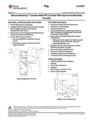
  • 1. UCC28060 1NATURAL INTERLEAVING FEATURES SYSTEM FEATURES APPLICATIONS +– COMP VREF PGNDAGND VCC ZCDA ZCDB GDA CS GDB VINAC VSENSE PWMCNTL UCC28061 TSET PHB HVSEN EMI Filter 400 VDC Power Good to downstream converter 85-265VAC Input Voltage (V) 5 4 3 2 1 70 120 170 220 270 CapacitorRippleCurrent(A) P = 600 W V = 400 V OUT OUT 1-Phase TM 2-Phase TM Interleave 1-Phase CCM UCC28061 www.ti.com .............................................................................................................................................................. SLUS837A–JUNE 2008–REVISED JULY 2009 Natural Interleaving™ Transition-Mode PFC Controller With Improved Audible Noise Immunity • Improved Audible Noise Performance23• Phase Management Capability • Soft Start on Overvoltage• FailSafe OVP with Dual Paths Prevents Output • Integrated BrownoutOver-Voltage Conditions Caused by Voltage-Sensing Failures • Improved Efficiency and Design Flexibility over Traditional, Single-Phase Continuous• Sensorless Current Shaping Simplifies Board Conduction Mode (CCM)Layout and Improves Efficiency • Input Filter and Output Capacitor Current• Inrush Safe Current Limiting: Cancellation: – Prevents MOSFET conduction during – Reduced current ripple for higher system inrush reliability and smaller bulk capacitor – Eliminates reverse recovery events in – Reduced EMI filter size output rectifiers • Enables Use of Low-Cost Diodes without Extensive Snubber Circuitry • Improved Light-Load Efficiency • Improved Transient Response • Complete System-Level Protection • 1-A Source/1.8-A Sink Gate Drivers • 100-W to 800-W Power Supplies • Gaming • D to A Set Top Boxes • Adapters • LCD, Plasma and DLP™ TVs • Home Audio Systems Typical Application Circuit Ripple Current Reduction 1 Please be aware that an important notice concerning availability, standard warranty, and use in critical applications of Texas Instruments semiconductor products and disclaimers thereto appears at the end of this data sheet. 2DLP is a trademark of Texas Instruments. 3Natural Interleaving is a trademark of Texas Instuments. PRODUCTION DATA information is current as of publication date. Copyright © 2008–2009, Texas Instruments Incorporated Products conform to specifications per the terms of the Texas Instruments standard warranty. Production processing does not necessarily include testing of all parameters.
  • 2. CONTENTS DESCRIPTION UCC28061 SLUS837A–JUNE 2008–REVISED JULY 2009 .............................................................................................................................................................. www.ti.com • Ordering Information 2 • Electrical Characteristics 4 • Device Information 7 • Functional Block Diagram 9 • Typical Characteristics 10 • Application Information 16 • Design Example 22 • Additional References 29 Optimized for consumer applications concerned with audible noise elimination, this solution extends the advantages of transition mode—high efficiency with low-cost components—to higher power ratings than previously possible. By utilizing a Natural Interleaving technique, both channels operate as masters (that is, there is no slave channel) synchronized to the same frequency. This approach delivers inherently strong matching, faster responses, and ensures that each channel operates in transition mode. Complete system-level protections feature input brownout, output over-voltage, open-loop, overload, soft-start, phase-fail detection, and thermal shutdown. The additional FailSafe over-voltage protection (OVP) feature protects against shorts to an intermediate voltage that, if undetected, could lead to catastrophic device failure. This integrated circuit can be damaged by ESD. Texas Instruments recommends that all integrated circuits be handled with appropriate precautions. Failure to observe proper handling and installation procedures can cause damage. ESD damage can range from subtle performance degradation to complete device failure. Precision integrated circuits may be more susceptible to damage because very small parametric changes could cause the device not to meet its published specifications. ORDERING INFORMATION(1) PART NUMBER PACKAGE(2) OPERATING TEMPERATURE RANGE, TA UCC28061D SOIC 16-Pin (D) –40°C to +125°C (1) For the most current package and ordering information see the Package Option Addendum at the end of this document, or see the TI web site at www.ti.com. (2) SOIC (D) package is available taped and reeled by adding R to the above part number. Reeled quantities for UCC28061DR are 2500 devices per reel. 2 Submit Documentation Feedback Copyright © 2008–2009, Texas Instruments Incorporated Product Folder Link(s): UCC28061
  • 3. ABSOLUTE MAXIMUM RATINGS(1) DISSIPATION RATINGS RECOMMENDED OPERATING CONDITIONS ELECTROSTATIC DISCHARGE (ESD) PROTECTION UCC28061 www.ti.com .............................................................................................................................................................. SLUS837A–JUNE 2008–REVISED JULY 2009 All voltages are with respect to GND, –40°C < TJ = TA < +125°C, and currents are positive into and negative out of the specified terminal, unless otherwise noted. UCC28061 UNIT VCC(2) –0.5 to +21 PWMCNTL –0.5 to +20 Input voltage range V COMP(3) , CS, PHB, HVSEN(4) , VINAC(4) , VSENSE(4) –0.5 to +7 ZCDA, ZCDB –0.5 to +4 Continuous input current VCC 20 Input current PWMCNTL 10 Input current range ZCDA, ZCDB, VSENSE –5 to +5 mA Output current VREF –10 Continuous gate current GDA, GDB(5) ±25 Operating –40 to +125 Junction temperature, TJ Storage –65 to +150 °C Lead temperature, TSOL Soldering, 10s +260 (1) Stresses beyond those listed under absolute maximum ratings may cause permanent damage to the device. These are stress ratings only and functional operation of the device at these or any other condition beyond those included under recommended operating conditions is not implied. Exposure to absolute-maximum-rated conditions for extended periods of time may affect device reliability. (2) Voltage on VCC is internally clamped. VCC may exceed the absolute maximum input voltage if the source is current limited below the absolute maximum continuous VCC input current level. (3) In normal use, COMP is connected to capacitors and resistors and is internally limited in voltage swing. (4) In normal use, VINAC, VSENSE, and HVSEN are connected to resistors and are internally limited in voltage swing. Although not recommended for extended use, VINAC, VSENSE, and HVSEN can survive input currents as high as ±10 mA from high voltage sources. (5) No GDA or GDB current limiting is required when driving a power MOSFET gate. However, a small series resistor may be required to damp ringing due to stray inductance. See Figure 12 and Figure 13 for details. THERMAL IMPEDANCE PACKAGE JUNCTION-TO-AMBIENT TA = +25°C POWER RATING TA = +85°C POWER RATING SOIC 16-Pin (D) 140°C/W(1) 890 mW(1) 460 mW(1) (1) Tested per JEDEC EIA/JESD 51-1. Thermal resistance is a strong function of board construction and layout. Air flow will reduce thermal resistance. This number is only a general guide; see TI document SPRA953 device Thermal Metrics. All voltages are with respect to GND, –40°C < TJ = TA < +125°C, and currents are positive into and negative out of the specified terminal, unless otherwise noted. MIN MAX UNIT VCC input voltage from a low-impedance source 14 21 V VCC input current from a high-impedance source 8 18 mA VREF load current 0 –2 VINAC Input voltage 0 6 V ZCDA, ZCDB series resistor 20 80 kΩ TSET resistor to program PWM on-time 66.5 400 HVSEN input voltage 0.8 4.5 V PWMCNTL pull-up resistor to VREF 1 10 kΩ RATING UNIT Human body model (HBM) 2000 V Charged device model (CDM) 500 V Copyright © 2008–2009, Texas Instruments Incorporated Submit Documentation Feedback 3 Product Folder Link(s): UCC28061
  • 4. ELECTRICAL CHARACTERISTICS UCC28061 SLUS837A–JUNE 2008–REVISED JULY 2009 .............................................................................................................................................................. www.ti.com At VCC = 16 V, AGND = PGND = 0 V, VINAC = 3 V, VSENSE = 6 V, HVSEN = 3 V, PHB = 5 V, RTSET = 133 kΩ; all voltages are with respect to GND, all outputs unloaded, –40°C < TJ = TA < +125°C, and currents are positive into and negative out of the specified terminal, unless otherwise noted. PARAMETER TEST CONDITIONS MIN TYP MAX UNIT VCC BIAS SUPPLY VCC(shunt) VCC shunt voltage(1) IVCC = 10 mA 22 24 26 V IVCC(stby) VCC current, disabled VSENSE = 0 V 100 200 µA IVCC(on) VCC current, enabled VSENSE = 6 V 5 8 mA UNDERVOLTAGE LOCKOUT (UVLO) VCC(on) VCC turn-on threshold 11.5 12.6 13.5 VCC(off) VCC turn-off threshold 9.5 10.35 11.5 V UVLO Hysteresis 1.85 2.25 2.65 REFERENCE VREF VREF output voltage, no load IVREF = 0 mA 5.82 6.00 6.18 V VREF change with load 0 mA ≤ IVREF ≤ –2 mA 1 6 mV VREF change with VCC 12 V ≤ VCC ≤ 20 V 1 10 ERROR AMPLIFIER VSENSE input regulation voltage TA = +25°C 5.85 6.00 6.15 V VSENSE input regulation voltage 5.82 6.00 6.18 VSENSE input bias current In regulation 125 300 800 nA COMP high voltage, clamped VSENSE = 5.8 V 4.70 4.95 5.10 V COMP low voltage, saturated VSENSE = 6.2 V 0.03 0.125 COMP = 3 V, gm VSENSE to COMP transconductance 75 96 110 µS 5.94 V < VSENSE < 6.06 V COMP source current, overdriven VSENSE = 5 V, COMP = 3 V –120 –160 –190 µA COMP sink current VSENSE = 6.2 V, COMP = 3 V 7 20 32 VSENSE threshold for COMP offset enable, down Voltage below VREF 135 185 235 mV from VREF VOVP VSENSE over-voltage threshold, rising 6.25 6.45 6.7 VSENSE over-voltage hysteresis 0.1 0.2 0.4 V VSENSE enable threshold, rising 1.15 1.25 1.35 VSENSE enable hysteresis 0.02 0.05 0.2 OUTPUT MONITORING VPWMCNTL HVSEN threshold to PWMCNTL HVSEN rising 2.35 2.50 2.65 V HVSEN input bias current, high HVSEN = 3 V –0.5 0.5 µA HVSEN input bias current, low HVSEN = 2 V 28 36 41 HVSEN rising threshold to over-voltage fault 4.64 4.87 5.1 V HVSEN falling threshold to over-voltage fault 4.45 4.67 4.80 PHB = 5 V, Phase Fail filter time to PWMCNTL high 8 12 20 ms ZCDA switching, ZCDB = 0.5 V PWMCNTL leakage current high HVSEN = 2 V, PWMCNTL = 15 V –1 1 µA PWMCNTL output voltage low HVSENS = 3 V, IPWMCNTL = 5 mA 0.2 0.5 V (1) Excessive VCC input voltage and current will damage the device. This clamp does not protect the device from an unregulated supply. If an unregulated supply is used, a Fixed Positive Voltage Regulator such as the UA78L15A is recommended. See the Absolute Maximum Ratings table for the limits on VCC voltage and current. 4 Submit Documentation Feedback Copyright © 2008–2009, Texas Instruments Incorporated Product Folder Link(s): UCC28061
  • 5. UCC28061 www.ti.com .............................................................................................................................................................. SLUS837A–JUNE 2008–REVISED JULY 2009 ELECTRICAL CHARACTERISTICS (continued) At VCC = 16 V, AGND = PGND = 0 V, VINAC = 3 V, VSENSE = 6 V, HVSEN = 3 V, PHB = 5 V, RTSET = 133 kΩ; all voltages are with respect to GND, all outputs unloaded, –40°C < TJ = TA < +125°C, and currents are positive into and negative out of the specified terminal, unless otherwise noted. PARAMETER TEST CONDITIONS MIN TYP MAX UNIT GATE DRIVE(2) GDA, GDB output voltage high IGDA, IGDB = –100 mA 11.5 13 15 GDA, GDB output voltage high, clamped VCC = 20 V, IGDA, IGDB = –5 mA 12 13.5 15 V GDA, GDB output voltage high, low VCC VCC = 12 V, IGDA, IGDB = –5 mA 10 10.5 11.5 GDA, GDB on-resistance high IGDA, IGDB = –100 mA 8 14 Ω GDA, GDB output voltage low IGDA, IGDB = 100 mA 0.15 0.3 V GDA, GDB on-resistance low IGDA, IGDB = 100 mA 2 3 Ω Rise time 1 V to 9 V, CLOAD = 1 nF 18 30 ns Fall time 9 V to 1 V, CLOAD = 1 nF 12 25 GDA, GDB output voltage UV IGDA, IGDB = 2.5 mA 1.6 2 V ZERO CURRENT DETECTOR ZCDA, ZCDB voltage threshold, falling 0.8 1.0 1.2 ZCDA, ZCDB voltage threshold, rising 1.5 1.68 1.88 V ZCDA, ZCDB clamp, high IZCDA = +2 mA, IZCDB = +2 mA 2.6 3.0 3.4 ZCDA, ZCDB input bias current ZCDA = 1.4 V, ZCDB = 1.4 V –0.5 0.5 µA ZCDA, ZCDB clamp, low IZCDA = –2 mA, IZCDB = –2 mA –0.4 –0.2 0 V Respective gate drive output rising 10% ZCDA, ZCDB delay to GDA, GDB outputs(2) 45 100 ns from zero crossing input falling to 1 V CURRENT SENSE CS input bias current At rising threshold –150 –250 µA CS current limit rising threshold –0.18 –0.20 –0.22 V CS current limit falling threshold –0.005 –0.015 –0.029 From CS exceeding threshold –0.05 V to CS current limit response time(2) 60 100 ns GDx dropping 10% MAINS INPUT VINAC input bias current VINAC = 2 V –0.5 0.5 µA BROWNOUT VINAC brownout threshold VINAC falling 1.34 1.39 1.44 V VINAC brownout current VINAC = 1 V 5 7 9 µA VINAC fails to exceed the brownout VINAC brownout filter time 340 440 540 ms threshold for the brownout filter time (2) Refer to Figure 12, Figure 13, Figure 14, and Figure 15 in the Typical Characteristics for typical gate drive waveforms. Copyright © 2008–2009, Texas Instruments Incorporated Submit Documentation Feedback 5 Product Folder Link(s): UCC28061
  • 6. UCC28061 SLUS837A–JUNE 2008–REVISED JULY 2009 .............................................................................................................................................................. www.ti.com ELECTRICAL CHARACTERISTICS (continued) At VCC = 16 V, AGND = PGND = 0 V, VINAC = 3 V, VSENSE = 6 V, HVSEN = 3 V, PHB = 5 V, RTSET = 133 kΩ; all voltages are with respect to GND, all outputs unloaded, –40°C < TJ = TA < +125°C, and currents are positive into and negative out of the specified terminal, unless otherwise noted. PARAMETER TEST CONDITIONS MIN TYP MAX UNIT PULSE-WIDTH MODULATOR KTL On-time factor, phases A and B VINAC = 3.2 V, VSENSE = 5.8 V(3) 3.6 4.0 4.4 µs/VVINAC = 3.2 V, VSENSE = 5.8 V, KTLS On-time factor, single-phase, A 7.2 8 8.9 PHB = 0 V(3) Phase B to phase A on-time matching VSENSE = 5.8 V, VINAC = 3.2 V –6% 6% COMP = 0.25 V, VINAC = 1 V 1.2 2 2.7Zero-crossing distortion correction additional on µs time COMP = 0.25 V, VINAC = 0.1 V 12.6 20 29 PHB threshold falling, to single-phase operation To GDB output shutdown VINAC = 1.5 V 0.7 0.8 0.9 V PHB threshold rising, to two-phase operation To GDB output running VINAC = 1.5 V 0.9 1.0 1.1 T(min) Minimum switching period RTSET = 133 kΩ(3) 1.7 2.2 2.5 µs PWM restart time ZCDA = ZCDB = 2 V(4) 165 200 265 THERMAL SHUTDOWN Thermal shutdown temperature TJ, temperature rising(5) +160 °C Thermal restart temperature TJ, temperature falling(5) +140 (3) Gate drive on-time is proportional to VCOMP – 125 mV. The on-time proportionality factor, KT, is different in two-phase and single-phase modes. The on-time factor, KT, scales linearly with the value of RTSET. The minimum switching period is proportional to RTSET. (4) An output on-time is generated at both GDA and GDB if both ZCDA and ZCDB negative-going edges are not detected for the restart time. In single-phase mode, the restart time applies for the ZCDA input and the GDA output. (5) Thermal shutdown occurs at temperatures higher than the normal operating range. Device performance above the normal operating temperature is not specified or assured. 6 Submit Documentation Feedback Copyright © 2008–2009, Texas Instruments Incorporated Product Folder Link(s): UCC28061
  • 7. DEVICE INFORMATION ZCDA VREF GDA PGND VCC GDB CS PWMCNTL ZCDB VSENSE TSET PHB COMP AGND VINAC HVSEN 1 2 3 4 5 6 7 8 16 15 14 13 12 11 10 9 UCC28061 www.ti.com .............................................................................................................................................................. SLUS837A–JUNE 2008–REVISED JULY 2009 UCC28061D SOIC 16-Pin (D) Top View TERMINAL FUNCTIONS TERMINAL DESCRIPTION NAME NO. I/O Analog ground: Connect analog signal bypass capacitors, compensation components, and analog AGND 6 — signal returns to this pin. Connect the analog and power grounds at a single point to isolate high-current noise signals of the power components from interference with the low-current analog circuits. Error amplifier output: The error amplifier is a transconductance amplifier, so this output is a high-impedance current source. Connect voltage regulation loop compensation components from this pin to AGND. The on-time seen at the gate drive outputs is proportional to the voltage at this pin minus an offset of approximately 125 mV. During soft-start events (undervoltage, brownout, disable or output COMP 5 O over voltage), COMP is pulled low. Normal operation only resumes after the soft-start event clears and COMP has been discharged below 0.5 V, making sure that the circuit restarts with a low COMP voltage and a short on-time. Do not connect COMP to a low-impedance source that would interfere with COMP falling below 0.5 V. Current sense input: Connect the current sense resistor and the negative terminal of the diode bridge to this pin. Connect the return of the current sense resistor to the AGND pin with a separate trace. As input current increases, the voltage on CS goes more negative. This cycle-by-cycle over-current protection limits input current by turning off both gate driver (GDx) outputs when CS is more negative than the CS rising threshold (approximately –200 mV). The GD outputs remain low until CS falls to the CS 10 I CS falling threshold (approximately –15 mV). Current sense is blanked for approximately 100 ns following the falling edge of either GD output. This blanking filters noise that occurs when current switches from a power FET to a boost diode. In most cases, no additional current sense filtering is required. If filtering is required, the filter series resistance must be under 100 Ω to maintain accuracy. To prevent excessive negative voltage on the CS pin during inrush conditions, connect the current sensing resistor to the CS pin through a low value external resistor. GDA 14 O Channel A and channel B gate drive output: Connect these pins to the gate of the power FET for each phase through the shortest connection practical. If it is necessary to use a trace longer than 0.5 inch (12.6 mm) for this connection, some ringing may occur due to trace series inductance. This ringingGDB 11 O can be reduced by adding a 5-Ω to 10-Ω resistor in series with GDA and GDB. High voltage output sense: The UCC28061 incorporates FailSafe OVP so that any single failure does not allow the output to boost above safe levels. Output over-voltage is monitored by both VSENSE and HVSEN and shuts down the PWM if either pin exceeds the appropriate over-voltage threshold. Using two pins to monitor for over-voltage provides redundant protection and fault tolerance. HVSEN can also be used to enable a downstream power converter when the voltage on HVSEN is within the operating HVSEN 8 I region. Select the HVSEN divider ratio for the desired over-voltage and power-good thresholds. Select the HVSEN divider impedance for the desired power-good hysteresis. During operation, HVSEN must never fall below 0.8 V. Dropping HVSEN below 0.8 V puts the UCC28061 into a special test mode, used only for factory testing. A bypass capacitor from HVSEN to AGND is recommended to filter noise and prevent false over-voltage shutdown. Power ground for the integrated circuit: Connect this pin to AGND through a separate short trace to PGND 13 — isolate gate driver noise from analog signals. Phase B enable: This pin turns on/off channel B of the boost converter. The commanded on-time for channel A is immediately doubled when channel B is disabled, which helps to keep COMP voltage PHB 4 I constant during the phase management transient. The PHB pin allows the user to add external phase management circuitry if they desire. To disable phase management, connect the PHB pin to the VREF pin. Copyright © 2008–2009, Texas Instruments Incorporated Submit Documentation Feedback 7 Product Folder Link(s): UCC28061
  • 8. UCC28061 SLUS837A–JUNE 2008–REVISED JULY 2009 .............................................................................................................................................................. www.ti.com TERMINAL FUNCTIONS (continued) TERMINAL DESCRIPTION NAME NO. I/O PWM enable logic output: This open-drain output goes low when HVSEN is within the HVSEN good PWMCNTL 9 O region and the ZCDA and ZCDB inputs are switching correctly if operating in two-phase mode (see PHB Pin). Otherwise, PWMCNTL is high impedance. Timing set: PWM on-time programming input. Connect a resistor from TSET to AGND to set the TSET 3 I on-time versus COMP voltage and the minimum period at the gate drive outputs. Bias supply input: Connect this pin to a controlled bias supply of between 14 V and 21 V. Also connect a 0.1-µF ceramic bypass capacitor from this pin to PGND with the shortest possible board trace. This VCC 12 — supply powers all circuits in the device and must be capable of delivering 6 mA dc plus the transient power MOSFET gate charging current. Input ac voltage sense: For normal operation, connect this pin to a voltage divider across the rectified input power mains. When the voltage on VINAC remains below the brownout threshold for more than VINAC 7 I the brownout filter time, the device enters a brownout mode and both output drives are disabled. Select the input voltage divider ratio for the desired brownout threshold. Select the divider impedance for the desired brownout hysteresis. Voltage reference output: Connect a 0.1-µF ceramic bypass capacitor from this pin to AGND. VREF VREF 15 O turns off during VCC undervoltage and VSENSE disable to save supply current and increase efficiency. This 6 VDC reference can be used to bias other circuits requiring less than 2 mA of total supply current. Output dc voltage sense: Connect this pin to a voltage divider across the output of the power converter. The error amplifier reference voltage is 6 V. Select the output voltage divider ratio for the desired output voltage. Connect the ground side of this divider to ground through a separate short trace VSENSE 2 I for best output regulation accuracy and noise immunity. VSENSE can be pulled low by an open-drain logic output or 6-V logic output in series with a low-leakage diode to disable the outputs and reduce VCC current. If VSENSE is disconnected, open-loop protection provides an internal current source to pull VSENSE low, turning off the gate drivers. Zero current detection inputs: These inputs expect to see a negative edge when the inductor current in the respective phases go to zero. The inputs are clamped at 0 V and 3 V. Signals should be coupled ZCDA 16 I through a series resistor that limits the clamping current to less than ±3 mA. Connect these pins through a current limiting resistor to the zero crossing detection windings of the appropriate boost inductor. The inductor winding must be connected so that this voltage drops when inductor current decays to zero. When the inductor current drops to zero, the ZCD input must drop below the falling ZCDB 1 I threshold, approximately 1 V, to cause the gate drive output to rise. When the power MOSFET turns off, the ZCD input must rise above the rising threshold, approximately 1.7 V, to arm the logic for another falling ZCD edge. 8 Submit Documentation Feedback Copyright © 2008–2009, Texas Instruments Incorporated Product Folder Link(s): UCC28061
  • 9. 7VINAC +1.4V Brownout440ms Delay 7mA Crossover Notch Reduction Phase A On Time Control 3 1.68V/1V ZCDA + 1.68V/1V ZCDB + 16 1 Phase B On Time Control 2VSENSE + VREF gm 6V15 EN + 6.45V OV + 4.95V 300nA TSET STOPA STOPB 5 COMP 222mV Brownout EN UV + 12 VCC GDA 13 PGND UV 12.6V 10.35V 24V 11 GDB 14 + 13.5V PGND Interleave Control 4.87V 9 PWMCNTL 36mA 8 HVSEN Phase OK 2.5V + + HVSEN OV 10CS Overcurrent + OV OC TSD STOPA HVSENOV Burst Operation STOPB SinglePhase -0.2V/-0.015V OC +0.8V Single Phase 4 PHB 6 AGND Thermal ShutDown + 160C TJ TSD ZCA ZCB Phase Fail Detector 1.25V 13.5V OV EN UV 96ms UCC28061 www.ti.com .............................................................................................................................................................. SLUS837A–JUNE 2008–REVISED JULY 2009 BLOCK DIAGRAM Copyright © 2008–2009, Texas Instruments Incorporated Submit Documentation Feedback 9 Product Folder Link(s): UCC28061
  • 10. TYPICAL CHARACTERISTICS V Bias Supply Voltage VVCC - - 5.5 5.0 4.5 4.0 3.5 3.0 0 0 2 4 6 8 10 12 14 16 18 20 IBiasSupplyCurrentmA-VCC- VCC Turn-Off VCC Turn-On 2.5 2.0 1.5 1.0 0.5 T Temperature C°J - - 6.0 5.8 5.6 5.4 5.2 4.0 -40 -20 0 20 40 60 80 100 120 IBiasSupplyCurrentmA-VCC- 5.0 4.8 4.6 4.4 4.2 Operating T Temperature C°J - - 140 120 100 80 60 0 -40 -20 0 20 40 60 80 100 120 IBiasSupplyCurrentA-mVCC- 40 20 Disabled V Input Voltage VVSENSE - - 40 20 0 -20 -40 -60 -180 5.5 5.6 5.7 5.8 5.9 6.0 6.1 6.2 6.3 6.4 6.5 IOutputCurrentA-mCOMP- -80 -100 -120 -140 -160 Transconductance 96 Sm Sink Current 25 Am Input Regulation Voltage 0 A at 6.0 Vm COMP Offset Enable 165 mV Down from Regulation Voltage Source Current Overdriven -160 Am UCC28061 SLUS837A–JUNE 2008–REVISED JULY 2009 .............................................................................................................................................................. www.ti.com At VCC = 16 V, AGND = PGND = 0 V, VINAC = 3 V, VSENSE = 6 V, HVSEN = 3 V, PHB = 5 V, RTSET = 133 kΩ; all voltages are with respect to GND, all outputs unloaded, TJ = TA = +25°C, and currents are positive into and negative out of the specified terminal, unless otherwise noted. BIAS SUPPLY CURRENT BIAS SUPPLY CURRENT vs vs BIAS SUPPLY VOLTAGE TEMPERATURE Figure 1. Figure 2. BIAS SUPPLY CURRENT vs TEMPERATURE ERROR AMPLIFIER TRANSFER FUNCTION Figure 3. Figure 4. 10 Submit Documentation Feedback Copyright © 2008–2009, Texas Instruments Incorporated Product Folder Link(s): UCC28061
  • 11. T Temperature C°J - - 110 105 100 95 90 80 -40 -20 0 20 40 60 80 100 120 gTransconductances-mm- 85 5.94 V < V < 6.06 VSENSE V Output Voltage VCOMP - - 11 10 9 8 7 6 0 0 1 2 3 4 5 IOutputCurrentA-mCOMP- 5 4 3 2 1 V = 6.1 VSENSE T Temperature C°J - - 150 145 140 135 130 125 -40 -20 0 20 40 60 80 100 120 ICurrentSenseInputBiasCurrentA-mCS- V Input Voltage VVSENSE - - 440 400 360 320 280 240 0 0 0.6 1.2 1.8 2.4 3.0 3.6 4.2 4.8 5.4 6.0 IInputBiasCurrentnA-VSENSE- 200 160 120 80 40 UCC28061 www.ti.com .............................................................................................................................................................. SLUS837A–JUNE 2008–REVISED JULY 2009 TYPICAL CHARACTERISTICS (continued) At VCC = 16 V, AGND = PGND = 0 V, VINAC = 3 V, VSENSE = 6 V, HVSEN = 3 V, PHB = 5 V, RTSET = 133 kΩ; all voltages are with respect to GND, all outputs unloaded, TJ = TA = +25°C, and currents are positive into and negative out of the specified terminal, unless otherwise noted. ERROR AMPLIFIER TRANSCONDUCTANCE ERROR AMPLIFIER OUTPUT CURRENT vs vs TEMPERATURE OUTPUT VOLTAGE Figure 5. Figure 6. ERROR AMPLIFIER INPUT BIAS CURRENT CURRENT SENSE INPUT BIAS CURRENT vs vs INPUT VOLTAGE TEMPERATURE Figure 7. Figure 8. Copyright © 2008–2009, Texas Instruments Incorporated Submit Documentation Feedback 11 Product Folder Link(s): UCC28061
  • 12. V Input Voltage VZCD - - 5 4 3 0 0 0.5 1.0 1.5 2.0 2.5 3.0 3.5 4.0 IClampCurrentmA-ZCD- 2 1 V Input Voltage VZCD - - 0 -0.5 -1.0 -3.5 -0.4 -0.3 -0.2 -0.1 0 0.1 0.2 0.3 0.4 IClampCurrentmA-ZCD- -1.5 -2.0 -2.5 -3.0 Time ns- 14 12 10 -2 0 50 100 150 200 250 300 350 GateDriveOutputV- 8 6 4 2 0 V = 20 V and 12 V C = 4.7 nF CC LOAD GD Source Current: V = 20 V V = 12 V CC CC GD Voltage: V = 20 V V = 12 V CC CC 3.0 2.5 2.0 -1.0 GateDriveSourceCurrentA- 1.5 1.0 0.5 0 -0.5 T Temperature C°J - - 500 490 480 470 460 350 -40 -20 0 20 40 60 80 100 120 BrownoutFilterDelayTimems- 450 440 430 360 370 380 390 400 410 420 UCC28061 SLUS837A–JUNE 2008–REVISED JULY 2009 .............................................................................................................................................................. www.ti.com TYPICAL CHARACTERISTICS (continued) At VCC = 16 V, AGND = PGND = 0 V, VINAC = 3 V, VSENSE = 6 V, HVSEN = 3 V, PHB = 5 V, RTSET = 133 kΩ; all voltages are with respect to GND, all outputs unloaded, TJ = TA = +25°C, and currents are positive into and negative out of the specified terminal, unless otherwise noted. ZERO CURRENT DETECT CLAMP CURRENT ZERO CURRENT DETECT CLAMP CURRENT vs vs HIGH INPUT VOLTAGE LOW INPUT VOLTAGE Figure 9. Figure 10. BROWNOUT FILTER DELAY TIME GATE DRIVE RISING vs vs TEMPERATURE TIME Figure 11. Figure 12. 12 Submit Documentation Feedback Copyright © 2008–2009, Texas Instruments Incorporated Product Folder Link(s): UCC28061
  • 13. Time ns- 14 12 10 -2 0 20 40 60 80 100 120 140 GateDriveOutputV- 8 6 4 2 0 V = 20 V and 12 V C = 4.7 nF CC LOAD GD Sink Current: V = 20 V V = 12 V CC CC GD Voltage: V = 20 V V = 12 V CC CC 3.0 2.5 2.0 -1.0 GateDriveSourceCurrentA- 1.5 1.0 0.5 0 -0.5 Time ns- 7 6 5 -1 -25 50 100 150 200 250 300 ZCDInputV- 4 3 2 1 0 0 14 12 10 -2 GateDriveOutputV- 8 6 4 2 0 C = 4.7 nFLOAD ZCD Input Voltage GD Output: T = 40 C T = +25 C T = +125 C J - ° J J ° ° Time ns- 500 400 300 -300 -25 50 100 150 200 250 300 CurrentSenseInputmV- 200 100 0 -100 -200 0 14 12 10 -2 GateDriveOutputV- 8 6 4 2 0 C = 4.7 nFLOAD CS Input Voltage GD Output: T = 40 C T = +25 C T = +125 C J - ° J J ° ° V Bias Supply Voltage VVCC - - 15 14 13 12 11 10 8 10 11 12 13 14 15 16 17 18 19 20 GateDriveVoltageV- 9 R = 2.7 kWLOAD T = 40 C- °J T = +25 CJ ° T = +125 CJ ° UCC28061 www.ti.com .............................................................................................................................................................. SLUS837A–JUNE 2008–REVISED JULY 2009 TYPICAL CHARACTERISTICS (continued) At VCC = 16 V, AGND = PGND = 0 V, VINAC = 3 V, VSENSE = 6 V, HVSEN = 3 V, PHB = 5 V, RTSET = 133 kΩ; all voltages are with respect to GND, all outputs unloaded, TJ = TA = +25°C, and currents are positive into and negative out of the specified terminal, unless otherwise noted. GATE DRIVE FALLING GATE DRIVE RISING vs vs TIME TIME AND DELAY FROM ZCD INPUT Figure 13. Figure 14. GATE DRIVE FALLING GATE DRIVE OUTPUT HIGH vs vs TIME AND DELAY FROM CS INPUT VCC Figure 15. Figure 16. Copyright © 2008–2009, Texas Instruments Incorporated Submit Documentation Feedback 13 Product Folder Link(s): UCC28061
  • 14. Gate Drive Sink Current mA- 2.5 2.0 1.5 1.0 0 0 1 2 3 4 5 6 7 8 9 10 GateDriveVoltageV- 0.5 T = 40 C- °J T = +25 CJ ° T = +125 CJ ° T Temperature C°J - - 15 14 13 5 -40 -20 0 20 40 60 100 120 GateDriveVoltageV- 12 11 10 9 8 7 6 Clamped VCC 15 V³ Unclamped VCC = 12 V R = 2 kWLOAD 60 R Time Setting Resistor kWTSET - - 10 9 8 7 6 0 60 80 100 180 200 220 240 260 280 KOn-TimeFactors/V-mT- 5 4 3 2 1 120 140 160 KTL T Temperature C°J - - 9 8 7 0 -40 -20 0 20 40 60 80 100 120 KOn-TimeFactors/V-mTL- 6 5 4 3 2 1 R = 266 kWTSET R = 133 kWTSET R = 66 kWTSET UCC28061 SLUS837A–JUNE 2008–REVISED JULY 2009 .............................................................................................................................................................. www.ti.com TYPICAL CHARACTERISTICS (continued) At VCC = 16 V, AGND = PGND = 0 V, VINAC = 3 V, VSENSE = 6 V, HVSEN = 3 V, PHB = 5 V, RTSET = 133 kΩ; all voltages are with respect to GND, all outputs unloaded, TJ = TA = +25°C, and currents are positive into and negative out of the specified terminal, unless otherwise noted. GATE DRIVE OUTPUT IN UVLO GATE DRIVE HIGH VOLTAGE vs vs SINK CURRENT TEMPERATURE Figure 17. Figure 18. ON-TIME FACTOR ON-TIME FACTOR PHASE A AND B vs vs TIME SETTING RESISTOR TEMPERATURE Figure 19. Figure 20. 14 Submit Documentation Feedback Copyright © 2008–2009, Texas Instruments Incorporated Product Folder Link(s): UCC28061
  • 15. Phase Shift of GDA Relative to GDB - Degrees 110 108 106 90 150 160 170 180 190 200 210 K/K%-TT0 104 102 100 98 96 94 92 R = 266 kWTSET R = 133 kWTSET R = 66 kWTSET K =T0 2(K K )´TA TB K + KTA TB GDA GDB T Temperature C°J - - 300 275 250 100 -40 -20 0 20 40 60 80 100 120 PWMRestartTimes-m 225 200 175 150 125 V Input AC Voltage Sense VVINAC - - 100 0.1 0 0.5 1.0 1.5 2.0 2.5 3.0 AdditionalOn-Times-m 10 1 R = 266 kTSET W R = 133 kTSET W R = 66 kWTSET UCC28061 www.ti.com .............................................................................................................................................................. SLUS837A–JUNE 2008–REVISED JULY 2009 TYPICAL CHARACTERISTICS (continued) At VCC = 16 V, AGND = PGND = 0 V, VINAC = 3 V, VSENSE = 6 V, HVSEN = 3 V, PHB = 5 V, RTSET = 133 kΩ; all voltages are with respect to GND, all outputs unloaded, TJ = TA = +25°C, and currents are positive into and negative out of the specified terminal, unless otherwise noted. ON-TIME FACTOR PWM RESTART TIME vs vs PHASE SHIFT TEMPERATURE Figure 21. Figure 22. ADDITIONAL ON-TIME vs VINAC ZERO-CROSSING DISTORTION CORRECTION Figure 23. Copyright © 2008–2009, Texas Instruments Incorporated Submit Documentation Feedback 15 Product Folder Link(s): UCC28061
  • 16. APPLICATION INFORMATION Theory of Operation I (t) =PEAK VINAC (t) T´ ON L (1) I (t) =AVG VINAC (t) T´ ON 2 L´ (2) On-Time Control, Maximum Frequency Limiting, and Restart Timer T = K (V 125 mV)-ON T COMP (3) T = K 4.825 V´ON(max) T (4) UCC28061 SLUS837A–JUNE 2008–REVISED JULY 2009 .............................................................................................................................................................. www.ti.com The UCC28061 contains the control circuits for two boost pulse-width modulation (PWM) power converters. The boost PWM power converters ramp current in the boost inductors for a time period proportional to the voltage on the error amplifier output. Each power converter then turns off the power MOSFET until current in the boost inductor decays to 0, as sensed on the zero current detection inputs (ZCDA and ZCDB). Once the inductor current decays to 0, the power converter starts another cycle. This on/off cycling produces a triangle wave of current, with peak current set by the on-time and power mains input voltage, as shown in Equation 1. The average line current is exactly equal to half of the peak line current, as shown in Equation 2. With TON and L being essentially constant during an ac line period, the resulting triangular current waveform during each switching cycle has an average value proportional to the instantaneous value of the rectified ac line voltage. This architecture results in a resistive input impedance characteristic at the line frequency and a near-unity power factor. The outputs of the two PWMs operate 180° out-of-phase so that power-line ripple current for the two PWMs is greatly reduced from the ripple current of each individual PWM. This design reduces ripple current at the input and output, allowing the reduction in size and cost of input and output filters. Optimal phase balance occurs if the individual power stages and the on-times are well-matched. Mismatches in inductor values do not affect the phase relationship. Gate drive on-time varies with the error amplifier output voltage by a factor called KT, as shown in Equation 3. Where: VCOMP is the output of the error amplifier, and 125 mV is a modulator offset. To provide smooth transition between two-phase and single-phase operation, KT increases by a factor of two in single-phase mode: • KTLS = 2 × KTL; active in single-phase operation The clamped maximum output of the error amplifier is limited to 4.95 V. This value, less the 125 mV modulator offset, limits on-time to Equation 4. This on-time limit sets the maximum power that can be delivered by the converter at a given input voltage level. The switching frequency of each phase is limited by minimum period timers. If the current decays to 0 before the minimum period timer elapses, turn-on is delayed, resulting in discontinuous phase current. The restart timer ensures starting under all circumstances by restarting both phases if either phase ZCD input has not transitioned high-to-low for approximately 200 µs. To prevent the circuit from operating in continuous conduction mode (CCM), the restart time does not trigger turn-on until both phase currents return to 0. 16 Submit Documentation Feedback Copyright © 2008–2009, Texas Instruments Incorporated Product Folder Link(s): UCC28061
  • 17. K =TL RTSET 133 kW ´ 4.0 ms V (5) T =MIN RTSET 133 kW ´ 2.2ms; Minimum Switching Period (6) Natural Interleaving Phase Management UCC28061 www.ti.com .............................................................................................................................................................. SLUS837A–JUNE 2008–REVISED JULY 2009 The on-time factors (KTH, KTHS, KTL, KTLS) and the minimum switching period TMIN are proportional to the time setting resistor RTSET, the resistor from the TSET pin to ground, and they can be calculated by Equation 5 through Equation 6: The proper value of RTSET results in the clamped maximum on-time, TON(max), required by the converter operating at the minimum input line and maximum load. Under normal operating conditions, the UCC28061 regulates the relative phasing of the channel A and channel B inductor currents to be very close to 180°, minimizing the ripple currents seen at the line source and output capacitor. The phase control function differentially modulates the on-times of the A and B channels based on the phase and frequency relationship. This natural interleaving method allows the converter to achieve 180° phase shift and transition mode operation for both phases without the requirements on boost inductor tolerance. As a result, the current sharing of the A and B channels are proportional to the inductor tolerance. The best current sharing is achieved when both inductors are exactly the same value. At light load, it can improve efficiency to shut down one phase. Although conduction losses increase in one-phase operation, switching losses decrease. At certain power levels, the reduction of switching losses is greater than the increase in conduction losses. Turning off one phase at light load is especially valuable for meeting light-load efficient standards. To operate in two-phase (normal) mode, pull PHB high or connect PHB to VREF. To operate in one-phase mode, connect PHB to ground. Copyright © 2008–2009, Texas Instruments Incorporated Submit Documentation Feedback 17 Product Folder Link(s): UCC28061
  • 18. Zero Crossing Detection and Valley Switching R C ZCD CT R1 C R2 ZCD CT Brownout Protection Failsafe OVP—Output Over-Voltage Protection UCC28061 SLUS837A–JUNE 2008–REVISED JULY 2009 .............................................................................................................................................................. www.ti.com In transition-mode PFC circuits, the MOSFET turns on when the boost inductor current crosses 0. Because of the resonance between the boost inductor and the parasitic capacitor at the MOSFET drain node, part of the energy stored in the MOSFET junction capacitor can be recovered, reducing switching losses. Furthermore, when the rectified input voltage is less than half of the output voltage, all the energy stored in the MOSFET junction capacitor can be recovered and zero-voltage switching (ZVS) can be realized. By adding an appropriate delay, the MOSFET can be turned on at the valley of its resonating drain voltage (valley switching). In this way, the energy recovery can be maximized and switching loss is minimized. The RC time constant is generally derived empirically, but a good starting point is a value equal to 25% of the resonant period of the drain circuit. The delay can be realized by a simple RC filter, as shown in Figure 24. Because the ZCD pin is internally clamped, a more accurate delay can also be realized by using Figure 25. Figure 24. Simple RC Delay Circuit Figure 25. More Accurate Time Delay Circuit As the power line RMS voltage decreases, RMS input current increases to maintain the output voltage constant for a specific load. Brownout protection prevents the RMS input current from exceeding a safe operating level. Power line RMS voltage is sensed at VINAC. When the voltage applied to VINAC fails to exceed the brownout threshold for the brownout filter time, a brownout condition is detected and both gate drive outputs immediately pull low. During brownout, COMP is actively pulled low. Gate drive outputs remain low until the voltage on VINAC rises above the brownout threshold. After a brownout, the power stage soft-starts as COMP rises. The brownout detection threshold and its hysteresis are set by the voltage divider ratio and resistor values. Brownout protection is based on VINAC peak voltage; the threshold and hysteresis are also based on line peak voltage. The peak VINAC voltage can be easily translated into RMS value. Suggested resistor values for the voltage divider are 3 MΩ ±1% from the rectified input voltage to VINAC and 46.4 kΩ ±1% from VINAC to ground. These resistors set the typical thresholds for RMS line voltages, as shown in Table 1. Table 1. Brownout Thresholds THRESHOLD BROWNOUT (RMS) Falling 65 V Rising 79.8 V FailSafe OVP prevents any single failure from allowing the output to boost above safe levels. Redundant paths for output voltage sensing provide additional protection against output over-voltage. Over-voltage protection is implemented through two independent paths: VSENSE and HVSEN. The converter shuts down if either input senses an over-voltage condition. The output voltage can still maintain a safe level with either loop failure. The device is re-enabled when both sense inputs fall back into the normal range. At that time, the gate drive outputs resume switching under PWM control. Output over-voltage does not cause soft-start and the COMP pin is not discharged during an output over-voltage event. 18 Submit Documentation Feedback Copyright © 2008–2009, Texas Instruments Incorporated Product Folder Link(s): UCC28061
  • 19. Over-Current Protection Phase Fail Protection Distortion Reduction UCC28061 www.ti.com .............................................................................................................................................................. SLUS837A–JUNE 2008–REVISED JULY 2009 Under certain conditions (such as inrush, brownout recovery, and output overload), the PFC power stage sees large currents. It is critical that the power devices be protected from switching during these conditions. The conventional current sensing method uses a shunt resistor in series with the MOSFET source to sense the converter current, resulting in multiple ground points and high power dissipation. Furthermore, since no current information is available when the MOSFETs are off, the source resistor current sensing method requires repeated turn-ons of the MOSFETs during over-current conditions. As a result, the converter may temporarily operate in continuous current mode (CCM) and experience failures induced by excessive reverse recovery currents in the boost diode. The UCC28061 uses a single resistor to continuously sense the total inductor (input) current. This way, turn-on of the MOSFETs is completely avoided when the inductor currents are excessive. The drive to the MOSFETs is inhibited until total inductor current drops to near zero, precluding reverse recovery induced failures (these failures are most likely to occur when the ac line recovers from a brownout condition). Following an over-current condition, both MOSFETs are turned on in phase when the input current drops to near 0. Because two phase currents are temporarily operating in phase, set the over-current protection threshold to more than twice of each phase maximum current ripple value in order to allow a return to normal operation after an over-current event. The UCC28061 detects failure of one phase by monitoring the sequence of ZCD pulses. During normal two-phase operation, if one ZCD input remains idle for longer than approximately 14 ms while the other ZCD input switches normally, PWMCNTL goes high, indicating that the power stage is not operating correctly. During normal single-phase operation, phase failure is not monitored. On the UCC28061, phase failure is not monitored if COMP is below approximately 222 mV. Because of the resonance between the capacitance present across the drain-source of the switching MOSFET and the boost inductor, conventional transition mode power factor correction circuits may not be able to absorb power from the input line when the input voltage is around 0 V. This limitation results in waveform distortion and increased harmonic distortion. To reduce line current distortion to the lowest possible level, the UCC28061 increases switching MOSFET on-time when input voltage is around 0 V to increase the power absorption and compensate for this effect. Copyright © 2008–2009, Texas Instruments Incorporated Submit Documentation Feedback 19 Product Folder Link(s): UCC28061
  • 20. Improved Error Amplifier REF VSENSE + - COMP 4.95 V CZ RZ CP + + COMP VSENSE Soft Start 6V 5.8V 6.45V OV PWM Shutdown 100mA gm + R Q QS +0.5V Brownout EN UV OV UCC28061 SLUS837A–JUNE 2008–REVISED JULY 2009 .............................................................................................................................................................. www.ti.com The voltage error amplifier is a transconductance amplifier. Voltage loop compensation is connected from the error amplifier output, COMP, to analog ground, AGND. The recommended compensation network is shown in Figure 26. Figure 26. Typical Error Amplifier Compensation To improve the transient response, the error amplifier output current is increased by 100 µA when the error amp input is below 5.8 V, as shown in Figure 27. This increase allows faster charging of the compensation components following sudden load current increases (also refer to Figure 4 in the Typical Characteristics). Figure 27. Error Amplifier Block Diagram Showing Speed-Up and Latched Soft-Start The UCC28061 asserts soft start when output over-voltage is detected, pulling COMP to ground. This improves response to a change from heavy load to light load. 20 Submit Documentation Feedback Copyright © 2008–2009, Texas Instruments Incorporated Product Folder Link(s): UCC28061
  • 21. Open-Loop Protection Soft-Start Light-Load Operation Command for the Downstream Converter VCC Undervoltage Protection VCC UCC28061 www.ti.com .............................................................................................................................................................. SLUS837A–JUNE 2008–REVISED JULY 2009 If the feedback loop is disconnected from the device, a current source internal to the UCC28061 pulls the VSENSE pin voltage towards ground. When VSENSE falls below 1.20 V, the device is disabled. When disabled, supply current decreases, and both gate drive outputs and COMP are actively pulled low. The device is re-enabled when VSENSE rises above 1.25 V. At that time, the gate drive outputs begin switching under PWM control. The device can be externally disabled by grounding the VSENSE pin with an open-drain or open-collector driver. When disabled, device supply current drops and COMP is actively pulled low. When VSENSE is released, the device soft-starts. This disable method forces the device into standby mode and minimizes its power consumption. This feature is particularly useful when standby power is a key design aspect. If the feedback loop is disconnected from ground, the VSENSE voltage goes high. When VSENSE rises above the over-voltage protection threshold, both gate drive outputs go low, and COMP is actively pulled low. The device is re-enabled when VSENSE falls back into range. At that time, the gate drive outputs begin switching under PWM control. The VSENSE pin is internally clamped to protect the device from damage under this condition. The PWM gradually ramps from zero on-time to normal on-time as the compensation capacitor from COMP to AGND charges from a low level to the final value. This process implements a soft-start, with a time constant set by the output current of the error amplifier and the value of the compensation capacitors. In the event of a brownout, logic disable, or VCC undervoltage fault, COMP is actively pulled low so the PWM soft-starts after this event is cleared. The UCC28061 also asserts soft start when output over-voltage is detected. Even if a fault event happens very briefly, soft-start fully discharges the compensation components before resuming operation, ensuring soft-starting. See Figure 27 for details. As load current decreases, the error amplifier commands less input current by lowering the COMP voltage. If PHB (normally connected to COMP) falls below 0.8 V at low input line (or 1.1 V at high input line), channel B stops switching and channel A on-time doubles to compensate. If COMP falls below 150 mV, channel A also stops switching and the loop enters a hysteretic control mode. The PWM skips cycles to maintain regulation. Instead of skipping cycles, the UCC28061 allows on-time reduction smoothly to zero as load decreases. However, maximum switching frequency is limited, so at very light load, discountinuous operation is possible. In the UCC28061, the PWMCNTL pin is used to coordinate the PFC stage with a downstream converter. Through the HVSEN pin, the output voltage is sensed. When the output voltage is within the desired range, the PWMCNTL pin is pulled to ground internally and can be used to enable a downstream converter. The enable threshold and hysteresis can be adjusted independently through the voltage divider ratio and resistor values. The HVSEN pin is also used for the FailSafe over-voltage protection. When designing the voltage divider, make sure this FailSafe over-voltage protection level is set above normal operating levels. VCC must rise above the undervoltage threshold for the PWM to begin functioning. If VCC drops below the threshold during operation, both gate drive outputs and COMP are actively pulled low. VCC must rise above the threshold for PWM function to restart. VCC is connected to a bias supply of between 13 V and 21 V. When powered from a poorly-regulated supply, an external zener diode is recommended to prevent excessive current into VCC. Copyright © 2008–2009, Texas Instruments Incorporated Submit Documentation Feedback 21 Product Folder Link(s): UCC28061
  • 22. DESIGN EXAMPLE +– COMP VREF PGNDAGND VCC ZCDA ZCDB GDA CS GDB VINAC VSENSE PWMCNTL UCC28061 TSET PHB HVSEN R 100 W CIN 10 nF RZ CZ RS CP RT 16V 2.2 mF Q1 Q2 D1 D2 RZA RZB L1 L2 RG1 RG2 COUT RD RC RLOAD16 V RE RF RA RB 50 kW PWMCNTL 20 kW 20 kW 5 W 5 W CB CA F1 D3 2.2 mF CF3 CF2 RP Bridge VOUT CF4 22 pF CF5 22 pF Design Goals UCC28061 SLUS837A–JUNE 2008–REVISED JULY 2009 .............................................................................................................................................................. www.ti.com An example of the UCC28061 PFC controller in a two-phase transition mode interleaved PFC pre-regulator is shown in Figure 28. Figure 28. Typical Transition Mode Interleaved PFC Pre-Regulator The specifications for this design were chosen based on the power requirements of a 300-W LCD TV. These specifications are shown in Table 2. Table 2. Design Specifications PARAMETER MIN TYP MAX UNIT 265 VIN RMS input voltage 85 (VIN_MIN) VRMS(VIN_MAX) VOUT Output voltage 390 V fLINE Line frequency 47 63 Hz PF Power factor at maximum load 0.90 POUT 300 W η Full load efficiency 0.92 fMIN Minimum switching frequency 45 kHz 22 Submit Documentation Feedback Copyright © 2008–2009, Texas Instruments Incorporated Product Folder Link(s): UCC28061
  • 23. Recommended PCB Device Layout CF4 UCC28061 www.ti.com .............................................................................................................................................................. SLUS837A–JUNE 2008–REVISED JULY 2009 Interleaved transition-mode PFC system architecture dramatically reduces input and output ripple current, allowing the circuit to use smaller and less expensive filters. To maximize the benefits of interleaving, the input and output filter capacitors should be located after the two phase currents are combined together. Similar to other power management devices, when laying out the printed circuit board (PCB) it is important to use star grounding techniques and keep filter capacitors as close to device ground as possible. To minimize the interference caused by capacitive coupling from the boost inductor, the device should be located at least 1 in (25.4 mm) away from the boost inductor. It is also recommended that the device not be placed underneath magnetic elements. Because of the precise timing requirement, the timing setting resistor RT should be put as close as possible to the TSET pin and returned to the analog ground. See Figure 29 for a recommended component layout and placement. Figure 29. Recommended PCB Layout NOTE: PHB and VREF Pins are connected by a Jumper on the back of the board. Copyright © 2008–2009, Texas Instruments Incorporated Submit Documentation Feedback 23 Product Folder Link(s): UCC28061
  • 24. Inductor Selection D =PEAK_LOW_LINE V V- ÖOUT IN_MIN 2 VOUT » 0.69= 390 V 85 V- Ö2 390 V (7) L1 = L2 = h ´ V x DIN_MIN PEAK_LOW_LINE 2 P fOUT MIN´ » m340 H= 0.92(85 V) 0.692 300 W 45 kHz´ (8) I =LPEAK P ÖOUT 2 V ´ hIN_MIN = 300 W Ö2 85 V 0.92´ » 5.4 A (9) I =LRMS ILPEAK Ö6 = 5.4 A Ö6 » 2.2 A (10) V V- ÖOUT IN_MAX 2 2 V » 8= 390 V 265 V- Ö2 2 V NP NS = (11) ZCD Resistor Selection (RZA, RZB) V NOUT S N 3 mA´P » W16.3 k= 390 V 8 3 mA´ R = R ³ZA ZB (12) R = R = 2ZA ZB 0 kW (13) UCC28061 SLUS837A–JUNE 2008–REVISED JULY 2009 .............................................................................................................................................................. www.ti.com The boost inductor is selected based on the inductor ripple current requirements at the peak of low line. Selecting the inductor requires calculating the boost converter duty cycle at the peak of low line (DPEAK_LOW_LINE), as shown in Equation 7. The minimum switching frequency of the converter (fMIN) under low line conditions occurs at the peak of low line and is set between 25 kHz and 50 kHz to avoid audible noise. For this design example, fMIN was set to 45 kHz: The inductor for this design would have a peak current (ILPEAK) of 5.4 A, as shown in Equation 9, and an RMS current (ILRMS) of 2.2 A, as shown in Equation 10. This converter uses constant on-time (TON) and zero-current switching (ZCS) to set up the converter timing. Auxiliary windings off of L1 and L2 detect when the inductor currents are 0. Selecting the turns ratio in Equation 11 ensures that there is at least 2 V at the peak of high line to reset the ZCD comparator after every switching cycle. The turns-ratio of each auxiliary winding is: The minimum value of the ZCD resistors is selected based on the internal zener clamp maximum current rating of 3 mA, as shown in Equation 12. In this design the ZCD resistors were set to 20 kΩ, as shown in Equation 13. 24 Submit Documentation Feedback Copyright © 2008–2009, Texas Instruments Incorporated Product Folder Link(s): UCC28061
  • 25. HVSENSE V = V 0.90 351 V´ »OUT_OK OUT (14) R =E Hysteresis 36 Am = 108 V 36 Am = 3 MW (15) R =F = = 31.185 kW » W31.6 k 2.5 V V 2.5 V-OUT_OK RE - m36 A 2.5 V 351 V 2.5 V- 3 MW - m36 A (16) V =OUT_MIN = » 240 V 2.5 V (R + R )E F RF 2.5 V (3 M + 31.6 k )W W 31.6 kW (17) V =OV_FAILSAFE = » 467 V 4.87 V (R + R )E F RF 4.87 V (3 M + 31.6 k )W W 31.6 kW (18) UCC28061 www.ti.com .............................................................................................................................................................. SLUS837A–JUNE 2008–REVISED JULY 2009 The HVSENSE pin programs the PWMCNTL output of the UCC28061. The PWMCNTL open-drain output can be used to disable a downstream converter while the PFC output capacitor is charging. PWMCNTL starts in high impedance and pulls to ground when the HVSENSE increases above 2.5 V. Setting the point where PWMCNTL becomes active requires a voltage divider from the boost voltage to the HVSEN pin to ground. Equation 14 to Equation 18 show how to set the PWMCNTL pin to activate when the output voltage is within 90% of its nominal value. Resistor RE sets up the high side of the voltage divider and programs the hysteresis of the PWMCNTL signal. For this example, RE was selected to provide 108 V of hysteresis, as shown in Equation 15. Resistor RF is used to program the PWMCNTL active threshold, as shown in Equation 16. This PWMCNTRL output remains active until a minimum output voltage (VOUT_MIN) is reached, as shown in Equation 17. According to the resistor value, the FailSafe OVP threshold should be set according to Equation 18: Copyright © 2008–2009, Texas Instruments Incorporated Submit Documentation Feedback 25 Product Folder Link(s): UCC28061
  • 26. Output Capacitor Selection C ³OUT = » m147 F V (V )-OUT OUT_MIN 2 2 2 POUT h 1 fLINE (390 V) (240 V)- 2 2 2 300 W 0.92 1 47 Hz (19) C = 200 FmOUT (20) 2 1 2 300 14 4 0 92 390 4 47 200h p p m ´ ´ = = » ´ ´ ´ ´ ´ ´ ´ OUT RIPPLE OUT LINE OUT P W V V V f C . V Hz F (21) I =COUT_100Hz = = 0.591 A POUT V ´ h ÖOUT ´ 2 300 W 390 V 0.92´ ´ Ö2 (22) I =COUT_HF - (I )COUT_100 Hz 2 P 2OUT Ö2 2 ´ ´h VIN_MIN 4 VÖ IN_MIN2 9 Vp OUT 2 (23) I =COUT_HF - (0.591 A)2300 W 2´ Ö2 2 ´ ´0.92 85 V 4 85 VÖ ´2 9 390 Vp ´ 2 » 0.966 A (24) UCC28061 SLUS837A–JUNE 2008–REVISED JULY 2009 .............................................................................................................................................................. www.ti.com The output capacitor (COUT) is selected based on holdup requirements as shown in Equation 19. Two 100-µF capacitors were used in parallel for the output capacitor: For this size capacitor, the output voltage ripple (VRIPPLE) is approximately 11 V, as shown in Equation 21: In addition to hold-up requirements, a capacitor must be selected so that it can withstand the low-frequency RMS current (ICOUT_100 Hz) and the high-frequency RMS current (ICOUT_HF); see Equation 22 to Equation 24. High-voltage electrolytic capacitors generally have both a low- and a high-frequency RMS current rating on the product data sheets. 26 Submit Documentation Feedback Copyright © 2008–2009, Texas Instruments Incorporated Product Folder Link(s): UCC28061
  • 27. Selecting an RS for Peak Current Limiting I =PEAK » 13 A 2P (1.2)OUT Ö2 h ´ VIN_MIN 2 300 W 1.2´ Ö ´2 0.92 85 V´ = (25) R =S » W15 m 200 mV IPEAK 200 mV 13 A = (26) R =S ´ »15 m 0.22 WW 300 W 85 V 0.92´ 2 P =RS POUT V ´ hIN_MIN 2 (27) ´ 5 s = 833 A s22.5 W 0.015 W I t =2 (28) Power Semiconductor Selection (Q1, Q2, D1, D2): I I = 13 A³DM PEAK (29) I =DS » 2.3 A 4 VÖ IN_MIN2 9 Vp ´ OUT IPEAK 2 1 6 - = 4 85 VÖ ´2 9 390 Vp ´ 13 A 2 1 6 - (30) I =D » 1.4 A 4 VÖ IN_MIN2 9 Vp ´ OUT IPEAK 2 = 4 85 VÖ ´2 9 390 Vp ´ 13 A 2 (31) UCC28061 www.ti.com .............................................................................................................................................................. SLUS837A–JUNE 2008–REVISED JULY 2009 The UCC28061 peak limit comparator senses the total input current and is used to protect the MOSFETs during inrush and over-load conditions. For reliability, the peak current limit (IPEAK) threshold in this design is set for 120% of the nominal inrush current that is observed during power-up, as shown in Equation 25. A standard 15-mΩ metal-film current-sense resistor is used for current sensing, as shown in Equation 26. The estimated power loss of the current sense resistor (PRS) is less than 0.25 W during normal operation, as shown in Equation 27. The most critical parameter in selecting a current-sense resistor is the surge rating. The resistor needs to withstand a short-circuit current larger than the current required to open the fuse (F1). I2 t (ampere squared seconds) is a measure of thermal energy resulting from current flow required to melt the fuse, where I2 t is equal to RMS current squared times the duration of the current flow in seconds. A 4-A fuse with an I2 t of 14 A2 s was chosen to protect the design from a short-circuit condition. To ensure the current-sense resistors have a high enough surge protection, a 15-MΩ, 500-mW, metal-strip resistor was chosen for the design. The resistor has a 2.5-W surge rating for 5 seconds. This result translates into 833 A2 s and has a high enough I2 t rating to survive a short-circuit before the fuse opens, as described in Equation 28. The selection of Q1, Q2, D1, and D2 are based on the power requirements of the design. Application note SLUU138, UCC38050 100-W Critical Conduction Power Factor Corrected (PFC) Pre-Regulator, explains how to select power semiconductor components for transition-mode PFC pre-regulators. The MOSFET maximum-pulsed drain current (Q1, Q2) is shown in Equation 29: The MOSFET RMS current calculation (Q1, Q2) is shown in Equation 30: To meet the power requirements of the design, IRFB11N50A 500-V MOSFETs were chosen for Q1 and Q2. The boost diode RMS current (D1, D2) is shown in Equation 31: To meet the power requirements of the design, MURS306T3 600-V diodes from On Semiconductor were chosen for the design for D1 and D2. Copyright © 2008–2009, Texas Instruments Incorporated Submit Documentation Feedback 27 Product Folder Link(s): UCC28061
  • 28. Brownout Protection R =A » W3 M Hysteresis 7 Am = 21 V 7 Am (32) R =B » W47 k 1.4 V R´ A V 0.75 1.4 V´ Ö -IN_MIN 2 = 1.4 V ´ W3 M 85 V 0.75 1.4 V´ Ö -2 (33) Converter Timing f =MIN = 39.2 kHz P L1OUT MAX´ = h (V )´ IN_MIN 2 V ÖIN_MIN ´ 2 VOUT 1 - 300 W 390 Hm´ 0.92 (85 V)´ 2 85 V Ö´ 2 390 V 1 - (34) R =TSET » W121 k 4.85 V 4 s fm´ ´ MIN = 133 kW V ÖIN_MIN ´ 2 VOUT 1 - 4.85 V 4 s 39.2 kHzm´ ´ 133 kW 85 V Ö´ 2 390 V 1 - (35) f =MAX » 550 kHz 2 s Rm ´ T = 133 kW 2 s 121 km W´ 133 kW (36) Programming VOUT R = 3 MWC (37) V = 6 VREF (38) R =D » W47 k (V V )-OUT REF = V RREF C´ (390 V 6V)- 6 V 3 M´ W (39) V = 6.45 VOVP = 418 V RD = 6.45 V R + RC D 47 kW 3 M + 47 kW W (40) UCC28061 SLUS837A–JUNE 2008–REVISED JULY 2009 .............................................................................................................................................................. www.ti.com Resistor RA and RB are selected to activate brownout protection at 75% of the specified minimum operated input voltage. Resistor RA programs the brownout hysteresis comparator, which was selected to provide 21 V of hysteresis. RA and RB are shown in Equation 32 and Equation 33. In this design example, brownout becomes active when the input drops below 64 VRMS and deactivates when the input reaches 79 VRMS. Select the timing resistor, RTSET, for the correct on-time (TON) based on KTL, as shown in Equation 34. To ensure proper operation, the timing must be set based on the highest boost inductance (L1MAX). In this design example, the boost inductor could be as high as 390 µH, based on line and load conditions, as shown in Equation 35. This result sets the maximum frequency clamp (fMAX), as shown in Equation 36, which improves efficiency at light load. Resistor RC is selected to minimize error because of VSENSE input bias current and minimize loading on the power line when the PFC is disabled. Construct resistor RC from two or more resistors in series to meet high-voltage requirements. RC was also selected to be of a similar value of RA and RE to simplify the bill of materials and reduce design costs. Based on the resistor values shown in Equation 37 to Equation 39, the primary output over-voltage protection threshold should be as shown in Equation 40: 28 Submit Documentation Feedback Copyright © 2008–2009, Texas Instruments Incorporated Product Folder Link(s): UCC28061
  • 29. Loop Compensation g = 96 Smm (41) H = » 0.015= VREF VOUT 6 V 390 V (42) R =Z = 6.313 k 6.34 k» WW= 100 mV V H gRIPPLE m´ ´ 100 mV 11 V 0.015 96 Sm´ ´ (43) C =Z = 2.67 Fm= 1 fLINE 5 2p ´ ´ RZ 1 47 Hz 5 2p ´ ´ W6.34 k (44) C =P = 1.12 nF= 1 fMIN 2 2p ´ ´ RZ 1 45 kHz 2 2p ´ ´ W6.34 k (45) C = 2.2 FmZ (46) C = 1 nFP (47) ADDITIONAL REFERENCES Related Parts References Package Outline and Recommended PCB Footprint UCC28061 www.ti.com .............................................................................................................................................................. SLUS837A–JUNE 2008–REVISED JULY 2009 Resistor RZ is sized to attenuate low-frequency ripple to less than 2% of the voltage amplifier output range. This value ensures good power factor and low input current harmonic distortion. The transconductance amplifier gain is shown in Equation 41: The voltage divider feedback gain is shown in Equation 42 and Equation 43: CZ is then set to add 45° of phase margin at 1/5th of the switching frequency, as shown in Equation 44: CP is sized to attenuate high-frequency noise, as shown in Equation 45: The standard values of Equation 46 and Equation 47 should be chosen for CZ and CP. Table 3 lists several TI parts that have characteristics similar to the UCC28061. Table 3. Related Parts DEVICE DESCRIPTION UCC28051 PFC controller for low to medium power applications UCC28019 8-pin continuous conduction mode (CCM) PFC controller UCC28060 Natural Interleaving™ Dual-Phase Transition-Mode PFC Controller These references, design tools, and links to additional references, including design software, may be found at www.power.ti.com: • Evaluation Module, UCC28060EVM 300W interleaved PFC Pre-regulator, SLUU280 from Texas Instruments • Application Note, UCC38050 100-W Critical Conduction Power Factor Corrected (PFC) Pre-regulator, SLUU138 from Texas Instruments The mechanical packages at the end of this data sheet outline the mechanical dimensions of the 16-pin D (SOIC) package and provide recommendations for PCB layout. Copyright © 2008–2009, Texas Instruments Incorporated Submit Documentation Feedback 29 Product Folder Link(s): UCC28061
  • 30. PACKAGE OPTION ADDENDUM www.ti.com 6-Feb-2020 Addendum-Page 1 PACKAGING INFORMATION Orderable Device Status (1) Package Type Package Drawing Pins Package Qty Eco Plan (2) Lead/Ball Finish (6) MSL Peak Temp (3) Op Temp (°C) Device Marking (4/5) Samples UCC28061D ACTIVE SOIC D 16 40 Green (RoHS & no Sb/Br) NIPDAU Level-1-260C-UNLIM -40 to 125 UCC28061 UCC28061DG4 ACTIVE SOIC D 16 40 Green (RoHS & no Sb/Br) NIPDAU Level-1-260C-UNLIM -40 to 125 UCC28061 UCC28061DR ACTIVE SOIC D 16 2500 Green (RoHS & no Sb/Br) NIPDAU Level-1-260C-UNLIM -40 to 125 UCC28061 (1) The marketing status values are defined as follows: ACTIVE: Product device recommended for new designs. LIFEBUY: TI has announced that the device will be discontinued, and a lifetime-buy period is in effect. NRND: Not recommended for new designs. Device is in production to support existing customers, but TI does not recommend using this part in a new design. PREVIEW: Device has been announced but is not in production. Samples may or may not be available. OBSOLETE: TI has discontinued the production of the device. (2) RoHS: TI defines "RoHS" to mean semiconductor products that are compliant with the current EU RoHS requirements for all 10 RoHS substances, including the requirement that RoHS substance do not exceed 0.1% by weight in homogeneous materials. Where designed to be soldered at high temperatures, "RoHS" products are suitable for use in specified lead-free processes. TI may reference these types of products as "Pb-Free". RoHS Exempt: TI defines "RoHS Exempt" to mean products that contain lead but are compliant with EU RoHS pursuant to a specific EU RoHS exemption. Green: TI defines "Green" to mean the content of Chlorine (Cl) and Bromine (Br) based flame retardants meet JS709B low halogen requirements of <=1000ppm threshold. Antimony trioxide based flame retardants must also meet the <=1000ppm threshold requirement. (3) MSL, Peak Temp. - The Moisture Sensitivity Level rating according to the JEDEC industry standard classifications, and peak solder temperature. (4) There may be additional marking, which relates to the logo, the lot trace code information, or the environmental category on the device. (5) Multiple Device Markings will be inside parentheses. Only one Device Marking contained in parentheses and separated by a "~" will appear on a device. If a line is indented then it is a continuation of the previous line and the two combined represent the entire Device Marking for that device. (6) Lead/Ball Finish - Orderable Devices may have multiple material finish options. Finish options are separated by a vertical ruled line. Lead/Ball Finish values may wrap to two lines if the finish value exceeds the maximum column width. Important Information and Disclaimer:The information provided on this page represents TI's knowledge and belief as of the date that it is provided. TI bases its knowledge and belief on information provided by third parties, and makes no representation or warranty as to the accuracy of such information. Efforts are underway to better integrate information from third parties. TI has taken and continues to take reasonable steps to provide representative and accurate information but may not have conducted destructive testing or chemical analysis on incoming materials and chemicals. TI and TI suppliers consider certain information to be proprietary, and thus CAS numbers and other limited information may not be available for release.
  • 31. PACKAGE OPTION ADDENDUM www.ti.com 6-Feb-2020 Addendum-Page 2 In no event shall TI's liability arising out of such information exceed the total purchase price of the TI part(s) at issue in this document sold by TI to Customer on an annual basis. OTHER QUALIFIED VERSIONS OF UCC28061 : •Automotive: UCC28061-Q1 NOTE: Qualified Version Definitions: •Automotive - Q100 devices qualified for high-reliability automotive applications targeting zero defects
  • 32. TAPE AND REEL INFORMATION *All dimensions are nominal Device Package Type Package Drawing Pins SPQ Reel Diameter (mm) Reel Width W1 (mm) A0 (mm) B0 (mm) K0 (mm) P1 (mm) W (mm) Pin1 Quadrant UCC28061DR SOIC D 16 2500 330.0 16.4 6.5 10.3 2.1 8.0 16.0 Q1 PACKAGE MATERIALS INFORMATION www.ti.com 29-Apr-2009 Pack Materials-Page 1
  • 33. *All dimensions are nominal Device Package Type Package Drawing Pins SPQ Length (mm) Width (mm) Height (mm) UCC28061DR SOIC D 16 2500 333.2 345.9 28.6 PACKAGE MATERIALS INFORMATION www.ti.com 29-Apr-2009 Pack Materials-Page 2
  • 34.
  • 35.
  • 36. IMPORTANT NOTICE AND DISCLAIMER TI PROVIDES TECHNICAL AND RELIABILITY DATA (INCLUDING DATASHEETS), DESIGN RESOURCES (INCLUDING REFERENCE DESIGNS), APPLICATION OR OTHER DESIGN ADVICE, WEB TOOLS, SAFETY INFORMATION, AND OTHER RESOURCES “AS IS” AND WITH ALL FAULTS, AND DISCLAIMS ALL WARRANTIES, EXPRESS AND IMPLIED, INCLUDING WITHOUT LIMITATION ANY IMPLIED WARRANTIES OF MERCHANTABILITY, FITNESS FOR A PARTICULAR PURPOSE OR NON-INFRINGEMENT OF THIRD PARTY INTELLECTUAL PROPERTY RIGHTS. These resources are intended for skilled developers designing with TI products. You are solely responsible for (1) selecting the appropriate TI products for your application, (2) designing, validating and testing your application, and (3) ensuring your application meets applicable standards, and any other safety, security, or other requirements. These resources are subject to change without notice. TI grants you permission to use these resources only for development of an application that uses the TI products described in the resource. Other reproduction and display of these resources is prohibited. No license is granted to any other TI intellectual property right or to any third party intellectual property right. TI disclaims responsibility for, and you will fully indemnify TI and its representatives against, any claims, damages, costs, losses, and liabilities arising out of your use of these resources. TI’s products are provided subject to TI’s Terms of Sale (www.ti.com/legal/termsofsale.html) or other applicable terms available either on ti.com or provided in conjunction with such TI products. TI’s provision of these resources does not expand or otherwise alter TI’s applicable warranties or warranty disclaimers for TI products. Mailing Address: Texas Instruments, Post Office Box 655303, Dallas, Texas 75265 Copyright © 2020, Texas Instruments Incorporated