Apresentação que aborda de modo geral o transistor de junção bipolar, desde seu contexto histórico até a sua constante aplicação na atualidade tecnológica.
Referências: <www.eletronicafacil.net>; <www.niltoncbraga.com.br>
Controlador Lógico Programável (CLP) ou do inglês PLC (Programmable Logic Controller) é um dos controladores mais utilizados na indústria. Conceitualmente, CLP é um equipamento projetado para comandar e monitorar máquinas ou processos industriais.Mais a fundo, é um computador especializado, baseado em um microprocessador que desempenha funções de controle através de softwares desenvolvidos pelo usuário (cada CLP tem seu próprio software)PB. É amplamente utilizado na indústria para o controlePE de diversos tipos e níveis de complexidade. Deve possuir um processador com software de controle e hardware que suporte operação em ambientes industriais. Este software, que é específico para automação e controle, possui um sistema operacional de tempo real, algo indispensável para controle de processos de alto risco como os que se encontram nas indústrias. Já o Hardware deve suportar as condições extremas de trocas temperatura, umidade, pressão entre outras situações as quais um computador padrão não suportaria.
ICL7660 Monolithic CMOS Voltage ConvertersGeorgage Zim
ICL7660 and ICL7660A contain all the necessary circuitry to complete a negative voltage converter, with the exception of 2 external capacitors which may be inexpensive 10μF polarized electrolytic types. Please visit for more information http://www.intersil.com/en/products/power-management/isolated-power/charge-pumps/ICL7660.html
Vaccine management system project report documentation..pdfKamal Acharya
The Division of Vaccine and Immunization is facing increasing difficulty monitoring vaccines and other commodities distribution once they have been distributed from the national stores. With the introduction of new vaccines, more challenges have been anticipated with this additions posing serious threat to the already over strained vaccine supply chain system in Kenya.
Immunizing Image Classifiers Against Localized Adversary Attacksgerogepatton
This paper addresses the vulnerability of deep learning models, particularly convolutional neural networks
(CNN)s, to adversarial attacks and presents a proactive training technique designed to counter them. We
introduce a novel volumization algorithm, which transforms 2D images into 3D volumetric representations.
When combined with 3D convolution and deep curriculum learning optimization (CLO), itsignificantly improves
the immunity of models against localized universal attacks by up to 40%. We evaluate our proposed approach
using contemporary CNN architectures and the modified Canadian Institute for Advanced Research (CIFAR-10
and CIFAR-100) and ImageNet Large Scale Visual Recognition Challenge (ILSVRC12) datasets, showcasing
accuracy improvements over previous techniques. The results indicate that the combination of the volumetric
input and curriculum learning holds significant promise for mitigating adversarial attacks without necessitating
adversary training.
NO1 Uk best vashikaran specialist in delhi vashikaran baba near me online vas...Amil Baba Dawood bangali
Contact with Dawood Bhai Just call on +92322-6382012 and we'll help you. We'll solve all your problems within 12 to 24 hours and with 101% guarantee and with astrology systematic. If you want to take any personal or professional advice then also you can call us on +92322-6382012 , ONLINE LOVE PROBLEM & Other all types of Daily Life Problem's.Then CALL or WHATSAPP us on +92322-6382012 and Get all these problems solutions here by Amil Baba DAWOOD BANGALI
#vashikaranspecialist #astrologer #palmistry #amliyaat #taweez #manpasandshadi #horoscope #spiritual #lovelife #lovespell #marriagespell#aamilbabainpakistan #amilbabainkarachi #powerfullblackmagicspell #kalajadumantarspecialist #realamilbaba #AmilbabainPakistan #astrologerincanada #astrologerindubai #lovespellsmaster #kalajaduspecialist #lovespellsthatwork #aamilbabainlahore#blackmagicformarriage #aamilbaba #kalajadu #kalailam #taweez #wazifaexpert #jadumantar #vashikaranspecialist #astrologer #palmistry #amliyaat #taweez #manpasandshadi #horoscope #spiritual #lovelife #lovespell #marriagespell#aamilbabainpakistan #amilbabainkarachi #powerfullblackmagicspell #kalajadumantarspecialist #realamilbaba #AmilbabainPakistan #astrologerincanada #astrologerindubai #lovespellsmaster #kalajaduspecialist #lovespellsthatwork #aamilbabainlahore #blackmagicforlove #blackmagicformarriage #aamilbaba #kalajadu #kalailam #taweez #wazifaexpert #jadumantar #vashikaranspecialist #astrologer #palmistry #amliyaat #taweez #manpasandshadi #horoscope #spiritual #lovelife #lovespell #marriagespell#aamilbabainpakistan #amilbabainkarachi #powerfullblackmagicspell #kalajadumantarspecialist #realamilbaba #AmilbabainPakistan #astrologerincanada #astrologerindubai #lovespellsmaster #kalajaduspecialist #lovespellsthatwork #aamilbabainlahore #Amilbabainuk #amilbabainspain #amilbabaindubai #Amilbabainnorway #amilbabainkrachi #amilbabainlahore #amilbabaingujranwalan #amilbabainislamabad
TECHNICAL TRAINING MANUAL GENERAL FAMILIARIZATION COURSEDuvanRamosGarzon1
AIRCRAFT GENERAL
The Single Aisle is the most advanced family aircraft in service today, with fly-by-wire flight controls.
The A318, A319, A320 and A321 are twin-engine subsonic medium range aircraft.
The family offers a choice of engines
Forklift Classes Overview by Intella PartsIntella Parts
Discover the different forklift classes and their specific applications. Learn how to choose the right forklift for your needs to ensure safety, efficiency, and compliance in your operations.
For more technical information, visit our website https://intellaparts.com
Automobile Management System Project Report.pdfKamal Acharya
The proposed project is developed to manage the automobile in the automobile dealer company. The main module in this project is login, automobile management, customer management, sales, complaints and reports. The first module is the login. The automobile showroom owner should login to the project for usage. The username and password are verified and if it is correct, next form opens. If the username and password are not correct, it shows the error message.
When a customer search for a automobile, if the automobile is available, they will be taken to a page that shows the details of the automobile including automobile name, automobile ID, quantity, price etc. “Automobile Management System” is useful for maintaining automobiles, customers effectively and hence helps for establishing good relation between customer and automobile organization. It contains various customized modules for effectively maintaining automobiles and stock information accurately and safely.
When the automobile is sold to the customer, stock will be reduced automatically. When a new purchase is made, stock will be increased automatically. While selecting automobiles for sale, the proposed software will automatically check for total number of available stock of that particular item, if the total stock of that particular item is less than 5, software will notify the user to purchase the particular item.
Also when the user tries to sale items which are not in stock, the system will prompt the user that the stock is not enough. Customers of this system can search for a automobile; can purchase a automobile easily by selecting fast. On the other hand the stock of automobiles can be maintained perfectly by the automobile shop manager overcoming the drawbacks of existing system.
CFD Simulation of By-pass Flow in a HRSG module by R&R Consult.pptxR&R Consult
CFD analysis is incredibly effective at solving mysteries and improving the performance of complex systems!
Here's a great example: At a large natural gas-fired power plant, where they use waste heat to generate steam and energy, they were puzzled that their boiler wasn't producing as much steam as expected.
R&R and Tetra Engineering Group Inc. were asked to solve the issue with reduced steam production.
An inspection had shown that a significant amount of hot flue gas was bypassing the boiler tubes, where the heat was supposed to be transferred.
R&R Consult conducted a CFD analysis, which revealed that 6.3% of the flue gas was bypassing the boiler tubes without transferring heat. The analysis also showed that the flue gas was instead being directed along the sides of the boiler and between the modules that were supposed to capture the heat. This was the cause of the reduced performance.
Based on our results, Tetra Engineering installed covering plates to reduce the bypass flow. This improved the boiler's performance and increased electricity production.
It is always satisfying when we can help solve complex challenges like this. Do your systems also need a check-up or optimization? Give us a call!
Work done in cooperation with James Malloy and David Moelling from Tetra Engineering.
More examples of our work https://www.r-r-consult.dk/en/cases-en/
Cosmetic shop management system project report.pdfKamal Acharya
Buying new cosmetic products is difficult. It can even be scary for those who have sensitive skin and are prone to skin trouble. The information needed to alleviate this problem is on the back of each product, but it's thought to interpret those ingredient lists unless you have a background in chemistry.
Instead of buying and hoping for the best, we can use data science to help us predict which products may be good fits for us. It includes various function programs to do the above mentioned tasks.
Data file handling has been effectively used in the program.
The automated cosmetic shop management system should deal with the automation of general workflow and administration process of the shop. The main processes of the system focus on customer's request where the system is able to search the most appropriate products and deliver it to the customers. It should help the employees to quickly identify the list of cosmetic product that have reached the minimum quantity and also keep a track of expired date for each cosmetic product. It should help the employees to find the rack number in which the product is placed.It is also Faster and more efficient way.
Overview of the fundamental roles in Hydropower generation and the components involved in wider Electrical Engineering.
This paper presents the design and construction of hydroelectric dams from the hydrologist’s survey of the valley before construction, all aspects and involved disciplines, fluid dynamics, structural engineering, generation and mains frequency regulation to the very transmission of power through the network in the United Kingdom.
Author: Robbie Edward Sayers
Collaborators and co editors: Charlie Sims and Connor Healey.
(C) 2024 Robbie E. Sayers
Industrial Training at Shahjalal Fertilizer Company Limited (SFCL)MdTanvirMahtab2
This presentation is about the working procedure of Shahjalal Fertilizer Company Limited (SFCL). A Govt. owned Company of Bangladesh Chemical Industries Corporation under Ministry of Industries.
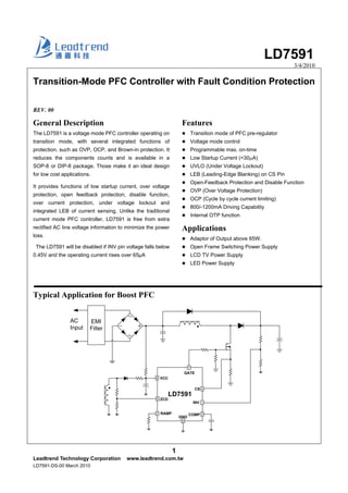
Original Transition-Mode PFC Controller IC LD7591GS 7591 SOP-8 New Leadtrend
1. LD7591
3/4/2010
1
Leadtrend Technology Corporation www.leadtrend.com.tw
LD7591-DS-00 March 2010
Transition-Mode PFC Controller with Fault Condition Protection
REV. 00
General Description
The LD7591 is a voltage mode PFC controller operating on
transition mode, with several integrated functions of
protection, such as OVP, OCP, and Brown-in protection. It
reduces the components counts and is available in a
SOP-8 or DIP-8 package. Those make it an ideal design
for low cost applications.
It provides functions of low startup current, over voltage
protection, open feedback protection, disable function,
over current protection, under voltage lockout and
integrated LEB of current sensing. Unlike the traditional
current mode PFC controller, LD7591 is free from extra
rectified AC line voltage information to minimize the power
loss.
The LD7591 will be disabled if INV pin voltage falls below
0.45V and the operating current rises over 65μA
Typical Application for Boost PFC
Features
Transition mode of PFC pre-regulator
Voltage mode control
Programmable max. on-time
Low Startup Current (<30μA)
UVLO (Under Voltage Lockout)
LEB (Leading-Edge Blanking) on CS Pin
Open-Feedback Protection and Disable Function
OVP (Over Voltage Protection)
OCP (Cycle by cycle current limiting)
800/-1200mA Driving Capability
Internal OTP function
Applications
Adaptor of Output above 65W.
Open Frame Switching Power Supply
LCD TV Power Supply
LED Power Supply
AC
Input
LD7591
8
5
3
7
4
6
GATE
CS
GND
ZCD
VCC
RAMP
EMI
Filter
1INV
2COMP
3. LD7591
3
Leadtrend Technology Corporation www.leadtrend.com.tw
LD7591-DS-00 March 2010
Pin Configuration
YY: Year code (D:2004, E:2005…)
WW: Week code
PP: Production code
1
8
2 3 4
7 6 5
TOP MARK
YYWWPP
INV
COMP
RAMP
CS
VCC
OUT
GND
ZCD
SOP-8 & DIP-8 (TOP VIEW)
Ordering Information
Part number Package Top Mark Shipping
LD7591 GS SOP-8 Green package LD7591GS 2500 /tape & reel
LD7591 GN DIP-8 Green package LD7591GN 3600 /tube /Carton
Pin Descriptions
Pin NAME FUNCTION
1 INV Output voltage feed back control
2 COMP Output of the error amplifier for voltage loop compensation to achieve stable
3 RAMP Ramp generator, connecting a resistor to GND pin to set the saw tooth signal
4 CS Current sense pin, connect to sense the MOSFET current for OCP
5 ZCD Detecting zero crossing of input signal
6 GND Ground
7 OUT Gate drive output to drive the external MOSFET
8 VCC Power source VCC pin
Recommended Operating Conditions
Item Min. Max. Unit
Vcc pin capacitor 22 47 μF
Comp pin capacitor 0.1 4.7 μF
RAMP pin resistor 4.7k 100k Ω
5. LD7591
5
Leadtrend Technology Corporation www.leadtrend.com.tw
LD7591-DS-00 March 2010
Absolute Maximum Ratings
Supply Voltage VCC -0.3 ~26V
OUT -0.3 ~VCC +0.3V
COMP, INV, CS, RAMP, ZCD -0.3 ~7V
Maximum Junction Temperature 150°C
Operating Junction Temperature Range -40°C to 125°C
Operating Ambient Temperature Range -40°C to 85°C
Storage Temperature Range -65°C to 150°C
Package Thermal Resistance (SO-8, θJA) 160°C/W
Package Thermal Resistance (DIP-8, θJA) 100°C/W
Power Dissipation (SOT-8, at Ambient Temperature = 85°C) 400mW
Power Dissipation (DIP-8, at Ambient Temperature = 85°C) 650mW
Lead temperature (Soldering, 10sec) 260°C
ESD Voltage Protection, Human Body Model 2.5 KV
ESD Voltage Protection, Machine Model 250 V
Gate Output Current 800mA/-1200mA
Caution:
Stresses beyond the ratings specified in “Absolute Maximum Ratings” may cause permanent damage to the device. This is a stress only
rating and operation of the device at these or any other conditions above those indicated in the operational sections of this specification
is not implied.
6. LD7591
6
Leadtrend Technology Corporation www.leadtrend.com.tw
LD7591-DS-00 March 2010
Electrical Characteristics
(VCC=14.0V, TA = 25°
C unless otherwise specified.)
PARAMETER CONDITIONS MIN TYP MAX UNITS
Supply Voltage (VCC Pin)
Startup Current VCC<UVLO ON 20 30 μA
VCOMP=0V 2.0 mA
VCOMP=3V 2.5 mA
VCC OVP 0.45 mA
Operating Current
(with 1nF load on OUT pin)
VINV=0V 65 95 μA
UVLO (off) 7.5 8.5 9.5 V
UVLO (on) 11.0 12.0 13.0 V
VCC OVP Level 19.5 21 22.5 V
Error Amplifier (Comp Pin)
Feedback Input Voltage, VREF 2.465 2.500 2.535 V
Input Bias Current VINV=1V~4V -0.5 0.5 μA
Transconductance 140 μmho
Output Sink Current VINV= VREF +0.1V 14 μA
Output Source Current VINV= VREF -0.1V -14 μA
Output Source Current VINV= VREF -0.5V -200 μA
Output Upper Clamp Voltage VINV= VREF -0.1V 5.4 5.9 6.4 V
0.95 VBurst Mode COMP pin Threshold
voltage Hysteresis 50 mV
INV pin
2.62 2.675 2.73 V
OVP Trip Level
OVP Hysteresis 0.175 V
0.4 0.45 0.5 V
Enable Threshold Voltage
Enable Hysteresis 0.1 V
Current Sensing (CS Pin)
Current Sense Input Threshold Voltage 0.75 0.8 0.85 V
Input bias current VCS=0V~1V 0 1.0 μA
LEB time 250 ns
Zero Current Detector (ZCD Pin)
Upper Clamp Voltage IDET=100μA 6.0 V
Lower Clamp Voltage IDET=100μA -0.7 V
0.05 0.1 0.15 V
Input Voltage Threshold
Hysteresis 0.1 V
Input bias current VZCD=1V~4V, OUT=OFF 0.0 1.0 μA
Maximum Delay from ZCD to Output 250 ns
7. LD7591
7
Leadtrend Technology Corporation www.leadtrend.com.tw
LD7591-DS-00 March 2010
PARAMETER CONDITIONS MIN TYP MAX UNITS
Maximum ON-Time, Ton-max (Ramp Pin)
Maximum On Time Voltage RRAMP=40.5K 2.784 2.900V 3.016 V
Maximum On Time Programming RRAMP =40.5K 19 24 29 μs
Maximum On Time RRAMP ≥ 100K 40 μs
Minimum OFF-Time
Minimum OFF-Time 1 μs
Minimum OFF-Time Programming 0.10
Ton-
max
Gate Drive Output (OUT Pin)
Output Low Level VCC=12V, ISINK=20mA 0.5 V
Output High Level VCC=12V, ISOURCE=20mA 9 12 V
Output High Clamp Level VCC=18V 13 V
Rising Time VCC =12V, CL=1000pF 75 150 ns
Falling Time VCC =12V, CL=1000pF 25 100 ns
Starter
Start Timer Period 50 150 300 μs
OTP (Over Temp. Protection)
OTP Trip level 140 °C
OTP Hysteresis 30 °C
8. LD7591
8
Leadtrend Technology Corporation www.leadtrend.com.tw
LD7591-DS-00 March 2010
Typical Performance Characteristics
UVLO(on)(V)
Fig. 1 UVLO (on) vs. Temperature
Temperature (°C)
11.0
11.5
12.0
12.5
13.0
13.5
-40 0 40 80 120 125
UVLO(off)(V)
Temperature (°C)
Fig. 2 UVLO (off ) vs. Temperature
7.5
8.5
9.0
10
8.0
-40 0 40 80 120 125
9.5
Istartup(μA)
Temperature (°C)
Fig. 3 Startup Current vs. Temperature
-40 0 40 80 120 125
20
22
24
26
28
18
30
VCCOVP(V)
Temperature (°C)
Fig. 4 VCC OVP vs. Temperature
10
15
20
25
30
35
-40 0 40 80 120 125
Vref(V)
Temperature (°C)
Fig. 5 Vref vs. Temperature
2.44
2.46
2.48
2.50
2.52
2.54
-40 0 40 80 120 125
INVOVP(V)
Temperature (°C)
Fig. 6 INV OVP vs. Temperature
2.5
2.55
2.6
2.65
2.7
2.75
-40 0 40 80 120 125
9. LD7591
9
Leadtrend Technology Corporation www.leadtrend.com.tw
LD7591-DS-00 March 2010
EnableVoltage(V)
Temperature (°C)
Fig. 7 Enable Voltage vs. Temperature
0.3
0.35
0.4
0.45
0.5
0.55
-40 0 40 80 120 125
VCS(off)(V)
Temperature (°C)
Fig. 8 VCS (off) vs. Temperature
0.78
0.79
0.80
0.81
0.82
0.83
-40 0 40 80 120 125
MaximumOn-TimeVoltage(V)
Temperature (°C)
Fig. 9 Maximum On-Time Voltage vs. Temperature
2.86
2.88
2.9
2.92
2.94
2.96
-40 0 40 80 120 125
MaximumOn-Time(μs)
Temperature (°C)
Fig. 10 Maximum On-Time vs. Temperature
-40 0 40 80 120 125
22
23
24
25
26
21
StartTimerPeriod(μs)
Temperature (°C)
Fig. 11 Start Timer Period vs. Temperature
140
145
150
155
160
165
-40 0 40 80 120 125
10. LD7591
10
Leadtrend Technology Corporation www.leadtrend.com.tw
LD7591-DS-00 March 2010
Application Information
Operation Overview
The LD7591 is an excellent voltage mode PFC controller.
It meets the IEC61000-3-2 requirement and is intended
for the use in those pre-regulator that demand low power
harmonics distortion. It integrated more functions to
reduce the external components counts and the size. Its
major features are described as below.
Under Voltage Lockout (UVLO)
An UVLO comparator is implemented in it to detect the
voltage on the VCC pin. It would assure the supply
voltage enough to turn on the LD7591 PFC controllers
and further to drive the power MOSFET. As shown in
Fig. 12, a hysteresis is built in to prevent the shutdown
from the voltage dip during start up. The turn-on and
turn-off threshold level are set at 12.0V and 8.5V,
respectively.
Vcc
UVLO(on)
UVLO(off)
t
t
I(Vcc)
startup current
(~uA)
operating current
(~ mA)
Fig. 12
Startup Current and Startup Circuit
The typical startup circuit to generate the LD7591 Vcc is
shown in Fig. 13. During the startup transient, the Vcc is
lower than the UVLO threshold thus there is no gate pulse
produced from LD7591 to drive power MOSFET.
Therefore, the current through R1 will provide the startup
current and to charge the capacitor C1. Whenever the
Vcc voltage is high enough to turn on the LD7591 and
further to deliver the gate drive signal, the supply current
is provided from the auxiliary winding of the PFC choke.
Lower startup current requirement on the PFC controller
will help to increase the value of R1 and then reduce the
power consumption on R1. By using CMOS process and
the special circuit design, the maximum startup current of
LD7591 is only 30μA. If a higher resistance value of R1 is
chosen, it usually takes more time to start up. To carefully
select the value of R1 and C1 will optimize the power
consumption and startup time.
Fig. 13
Output Voltage Setting
The LD7591 monitors the output voltage signal at INV pin
through a resistor divider pair Ra and Rb. A
transconductance amplifier is used instead of the
conventional voltage amplifier. The transconductance
amplifier (voltage controlled current source) aids the
implementation of OVP and disables function. The output
current of the amplifier changes according to the voltage
difference of the inverting and non-inverting input of the
amplifier. The output voltage of the amplifier is compared
with the internal ramp signal to generate the turn-off
signal. The output voltage is determined by the following
relationship.
)
Rb
Ra
1(V5.2VOUT +=
11. LD7591
11
Leadtrend Technology Corporation www.leadtrend.com.tw
LD7591-DS-00 March 2010
Where Ra and Rb are top and bottom feedback resistor
values (as shown in the Fig. 14).
Fig. 14
OVP and Disable on INV pin
To prevent the over voltage on the output capacitor from
the fault condition, LD7591 is implemented with an OVP
function on INV pin. Whenever the INV voltage is higher
than the OVP threshold voltage 2.675V, the output gate
drive circuit will be shutdown simultaneously thus to stop
the switching of the power MOSFET until the INV pin
down to 2.5V. The OVP function in LD7591 is an
auto-recovery type protection. The Fig. 15 shows its
operation. On the other hand, if the OVP condition is
removed, the Vcc level will get back to normal level and
the output will automatically return to the normal
operation.
The disable comparator disables the operation of the
LD7591 when the voltage of the inverting input is lower
than 0.35V and there is 100mV hysteresis. An external
small signal MOSFET can be used to disable the IC,
referring to Fig. 14. The IC operating current decreases
below 65μA to reduce power consumption if the IC is
disabled.
Fig. 15
Zero Current Detection (ZCD)
Fig. 16 shows typical ZCD-block. The Zero Current
Detection block will switch on the external MOSFET as
the current through the boost inductor drops to zero in
using an auxiliary winding coupled with the inductor. This
feature allows transition-mode operation. If the voltage of
the ZCD pin goes higher than 0.2V, the ZCD comparator
waits until the voltage rises above 0.1V. If the voltage
goes below 0.1V, the zero current detector will turn on the
MOSFET. The ZCD pin is protected internally by two
clamps, 6.0V-high clamp and -0.7V-low clamp. The
150μs timer generates a MOSFET turn on signal if the
driver output has been low for more than 150μs from the
falling edge of the driver output.
Fig. 16
12. LD7591
12
Leadtrend Technology Corporation www.leadtrend.com.tw
LD7591-DS-00 March 2010
Fig. 17 shows typical ZCD-related waveforms. Rz1 will
produce some delay because of the capacitance carried
by ZCD pin, it therefore delay the turn-on time accordingly.
The switch will be turned on when the inductor current
reaches zero; because of the structure of the ZCD delay,
it will be turned on after some delay time. During this
delay time, the stored charge of the COSS (MOSFET
output capacitor) will be discharged through the path
indicated in Fig. 18. This charge is transferred into a small
filter capacitor CIN1, which is connected to the bridge
diode. Therefore, there is no current flowing from the
input side. That is, the input current IIN is zero during this
period. In order to reduce the negative current flowing to
the internal diode, a larger resistance of RZ1 over 47kΩ is
recommended.
Fig. 17
Fig. 18
Ramp Generator Block
The output of the gm error amplifier and the output of the
ramp generator block are compared to determine the
MOSFET on time, as shown in Fig. 19. The slope of the
ramp is determined by an external resistor connected to
the RAMP pin. The voltage of the RAMP pin is 2.9V and
the slope is proportional to the current flowing out of the
RAMP pin. The internal ramp signal has a 1V offset;
therefore, the drive output will be shut down if the voltage
of the COMP pin is lower than 0.95V. The programmed
on-time will be at its maximum when the COMP pin is
open. The COMP pin open voltage is about 5.4~6.6V.
According to the slope of the internal ramp, the maximum
on-time can be programmed. The necessary maximum
on-time will be achieved depending on the boost inductor,
lowest AC line voltage, and maximum output power. The
resistor value should be designed properly. The
maximum on-time can be obtained from below
9
RAMP
)MAX(TimeON
1058.1
R
T
⋅
=−
Fig. 19
13. LD7591
13
Leadtrend Technology Corporation www.leadtrend.com.tw
LD7591-DS-00 March 2010
Output Drive Stage
An output stage of a CMOS buffer, with typical
800mA/-1200mA driving capability, is incorporated to
drive a power MOSFET directly. The output voltage is
clamped at 13V to protect the MOSFET gate even when
the VCC voltage is higher than 13V.
Current Sensing and Leading-edge
Blanking
The typical voltage mode of PFC controller feedbacks the
voltage signals to close the control loop and achieve
regulation. The LD7591 detects the primary MOSFET
current from the CS pin, which is for the pulse-by-pulse
current limit. The maximum voltage threshold of the
current sensing pin is set at 0.8V. From above, the
MOSFET peak current can be obtained from below.
S
)MAX(PEAK
R
V8.0
I =
A 250ns leading-edge blanking (LEB) time is included in
the input of CS pin to prevent the false-trigger from the
current spike. The R-C filter may be eliminated in some
low power applications, such as the pulse width of the
turn-on spikes is below 250ns and the negative spike on
the CS pin is below -0.3V.
However, the pulse width of the turn-on spike is
determined according to the output power, circuit design
and PCB layout. It is strongly recommended to adopt a
smaller R-C filter for higher power application to avoid the
CS pin being damaged by the negative turn-on spike.
Fig. 20
Fault Protection
There are several critical protections integrated in the
LD7591 to prevent the power supply or adapter from
being damaged. Those damages usually come from open
or short condition on the pins of LD7591.
Under the conditions listed below, the gate output will turn
off immediately to protect the power circuit ---
1. Ramp pin short to ground
2. Ramp pin floating
3. CS pin floating
18. LD7591
18
Leadtrend Technology Corporation www.leadtrend.com.tw
LD7591-DS-00 March 2010
Package Information
SOP-8
Dimensions in Millimeters Dimensions in Inch
Symbols
MIN MAX MIN MAX
A 4.801 5.004 0.189 0.197
B 3.810 3.988 0.150 0.157
C 1.346 1.753 0.053 0.069
D 0.330 0.508 0.013 0.020
F 1.194 1.346 0.047 0.053
H 0.178 0.229 0.007 0.009
I 0.102 0.254 0.004 0.010
J 5.791 6.198 0.228 0.244
M 0.406 1.270 0.016 0.050
θ 0° 8° 0° 8°
19. LD7591
19
Leadtrend Technology Corporation www.leadtrend.com.tw
LD7591-DS-00 March 2010
Package Information
DIP-8
Dimension in Millimeters Dimensions in Inches
Symbol
Min Max Min Max
A 9.017 10.160 0.355 0.400
B 6.096 7.112 0.240 0.280
C ----- 5.334 ------ 0.210
D 0.356 0.584 0.014 0.023
E 1.143 1.778 0.045 0.070
F 2.337 2.743 0.092 0.108
I 2.921 3.556 0.115 0.140
J 7.366 8.255 0.29 0.325
L 0.381 ------ 0.015 --------
Important Notice
Leadtrend Technology Corp. reserves the right to make changes or corrections to its products at any time without notice. Customers
should verify the datasheets are current and complete before placing order.