
Recommended
Recommended
More Related Content
What's hot
What's hot (20)
Similar to Original IGBT TGPF30N43P TGPF30N43 30N43 30N43P 450V 60A TO-220F New TRinno
Similar to Original IGBT TGPF30N43P TGPF30N43 30N43 30N43P 450V 60A TO-220F New TRinno (14)
More from AUTHELECTRONIC
More from AUTHELECTRONIC (20)
Recently uploaded
Recently uploaded (20)
Original IGBT TGPF30N43P TGPF30N43 30N43 30N43P 450V 60A TO-220F New TRinno
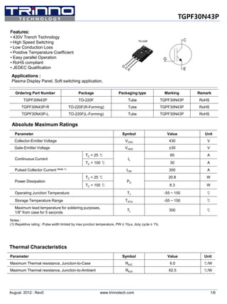
- 1. August 2012 : Rev0 1/6www.trinnotech.com TGPF30N43P Parameter Symbol Value Unit Collector-Emitter Voltage VCES 430 V Gate-Emitter Voltage VGES ±30 V Continuous Current TC = 25 ℃ Ic 60 A TC = 100 ℃ 30 A Pulsed Collector Current (Note 1) ICM 300 A Power Dissipation TC = 25 ℃ PD 20.8 W TC = 100 ℃ 8.3 W Operating Junction Temperature TJ -55 ~ 150 ℃ Storage Temperature Range TSTG -55 ~ 150 ℃ Maximum lead temperature for soldering purposes, 1/8” from case for 5 seconds TL 300 ℃ G C E C Parameter Symbol Value Unit Maximum Thermal resistance, Junction-to-Case RθJC 6.0 ℃/W Maximum Thermal resistance, Junction-to-Ambient RθJA 62.5 ℃/W Notes : (1) Repetitive rating : Pulse width limited by max junction temperature, PW ≤ 10µs, duty cycle ≤ 1%. Absolute Maximum Ratings Thermal Characteristics Features: • 430V Trench Technology • High Speed Switching • Low Conduction Loss • Positive Temperature Coefficient • Easy parallel Operation • RoHS compliant • JEDEC Qualification Applications : Plasma Display Panel, Soft switching application, Ordering Part Number Package Packaging type Marking Remark TGPF30N43P TO-220F Tube TGPF30N43P RoHS TGPF30N43P-R TO-220F(R-Forming) Tube TGPF30N43P RoHS TGPF30N43P-L TO-220F(L-Forming) Tube TGPF30N43P RoHS
- 2. 2/6www.trinnotech.comAugust 2012 : Rev0 TGPF30N43P Electrical Characteristics of the IGBT TC=25℃, unless otherwise noted Parameter Symbol Test condition Min Typ Max Units OFF Collector – Emitter Breakdown Voltage BVCES VGE = 0V, IC = 1mA 430 -- -- V Zero Gate Voltage Collector Current ICES VCE = 430V, VGE = 0V -- -- 100 µA Gate – Emitter Leakage Current IGES VCE = 0V, VGE = ±30V -- -- ± 250 nA ON Gate – Emitter Threshold Voltage VGE(TH) VGE = VCE, IC = 1mA 2 3.1 4.5 V Collector – Emitter Saturation Voltage VCE(SAT) VGE = 15V, IC = 30A, TJ = 25 oC -- 1.4 2.0 V VGE = 15V, IC = 30A, TJ = 125 oC -- 1.52 -- V DYNAMIC Input Capacitance CIES VCE = 25V, VGE = 0V, f = 1MHz -- 845 -- pF Output Capacitance COES -- 50 -- pF Reverse Transfer Capacitance CRES -- 23 -- pF SWITCHING Turn-On Delay Time td(on) VCC = 150V, IC = 30A, RG = 5Ω, VGE = 15V, Resistive Load, TJ = 25 oC -- 13 -- ns Rise Time tr -- 105 -- ns Turn-Off Delay Time td(off) -- 35 -- ns Fall Time tf -- 160 -- ns Turn-On Delay Time td(on) VCC = 150V, IC = 30A, RG = 5Ω, VGE = 15V, Resistive Load, TJ = 125 oC -- 14 -- ns Rise Time tr -- 145 -- ns Turn-Off Delay Time td(off) -- 40 -- ns Fall Time tf -- 240 -- ns Total Gate Charge Qg VCC = 150V, IC = 30A, VGE = 15V -- 26 -- nC Gate-Emitter Charge Qge -- 3.1 -- nC Gate-Collector Charge Qgc -- 9 -- nC
- 3. August 2012 : Rev0 3/6www.trinnotech.com TGPF30N43P 0 2 4 6 8 10 12 14 16 18 20 0 2 4 6 8 10 12 14 16 18 30A 90A 60A Collector-EmitterVoltage,VCE [V] Gate - Emitter Voltage, VGE [V] TC = 125 o C I C = 15A 0.1 1 10 0 200 400 600 800 1000 1200 Common Emitter VGE =0V, f=1MHz Tc =25 o C Capacitance[pF] Collector - Emitter Voltage, VCE [V] Cies Coes Cres Fig. 1 Output characteristics Fig. 2 Saturation voltage characteristics Fig. 3 Saturation voltage vs. collector current Fig. 4 Saturation voltage vs. gate bias Fig. 5 Saturation voltage vs. gate bias Fig. 6 Capacitance characteristics 0 1 2 3 4 5 0 30 60 90 120 150 VGE = 15V CollectorCurrent,Ic[A] Collector - Emitter Voltage, VCE [V] -25 o C 25 o C 125 o C -25 0 25 50 75 100 125 150 0.5 1.0 1.5 2.0 2.5 IC = 15A IC = 60A Collector-EmitterVoltage,VCE [V] Case Temperature, TC [ o C] VGE = 15V IC = 30A 0 2 4 6 8 10 12 14 16 18 20 0 2 4 6 8 10 12 14 16 18 30A 90A 60A Collector-EmitterVoltage,VCE [V] Gate - Emitter Voltage, VGE [V] TC = 25 o C I C = 15A 0 2 4 6 8 10 0 50 100 150 200 6V 7V 8V 9V 11V 15V 20V CollectorCurrent,Ic[A] Collector - Emitter Voltage, VCE [V] VGE = 5V 10V Tc = 25 o C 12V
- 4. August 2012 : Rev0 4/6www.trinnotech.com TGPF30N43P Fig. 7 Turn on time vs. gate resistance Fig. 8 Turn on time vs. collector current Fig. 9 Turn on time vs. Case temperature Fig. 10 Turn off time vs. gate resistance Fig. 11 Turn off time vs. collector current Fig. 12 Turn off time vs. Case temperature 0 20 40 60 80 100 1 10 100 1000 Common Emitter Vcc = 150V, VGE = 15V, IC = 30A TC 25 o C TC 125 o C Td(on) SwitchingTime[ns] Gate Resistance, RG [Ω] Tr 0 20 40 60 80 100 10 100 1000 Common Emitter Vcc = 150V, VGE = 15V, IC = 30A TC 25 o C TC 125 o C Td(off) SwitchingTime[ns] Gate Resistance, RG [Ω] Tf 10 20 30 40 50 60 70 80 90 1 10 100 1000 Collector Current, IC [A] Common Emitter Vcc = 150V, VGE = 15V, RG = 5Ω TC 25 o C TC 125 o C Td(off) SwitchingTime[ns] Tf 40 60 80 100 120 1 10 100 Common Emitter Vcc = 150V, VGE = 15V, RG = 5Ω, IC = 30A Td(on) Tr SwitchingTime[ns] Case Temperature, TC [ o C] 40 60 80 100 120 10 100 Common Emitter Vcc= 150V, VGE = 15V, RG = 5Ω, IC = 30A Tf Td(off) SwitchingTime[ns] Case Temperature, TC [ o C] 10 20 30 40 50 60 70 80 90 1 10 100 1000 Common Emitter Vcc = 150V, VGE = 15V, RG = 5Ω TC 25 o C TC 125 o C Td(on) SwitchingTime[ns] Collector Current, IC [A] Tr
- 5. August 2012 : Rev0 5/6www.trinnotech.com TGPF30N43P Fig. 13 Gate charge characteristics Fig. 14 SOA Fig. 15 RBSOA Fig. 16 Transient thermal impedance 1E-5 1E-4 1E-3 0.01 0.1 1 10 0.01 0.1 1 10 Duty = 0.5 0.1 0.2 0.05 0.01 0.02 ThermalRespose[Zthjc] Rectangular Pulse Width [sec] single pulse 0.1 1 10 100 1000 0.01 0.1 1 10 100 1000 TC = 25 o C TJ = 150 o C Single Pulse 1ms 10ms 10us 100us DC IC Max (pulsed) CollectorCurrent,IC [A] Collector - Emitter Voltage, VCE [V] IC Max (continuous) 0 5 10 15 20 25 30 0 5 10 15 VGE = 15V, IC = 30A, TC = 25 o C VCE = 150V VCE = 200V VCE = 320V Gate-EmitterVoltage,VGE [V] Gate Charge, QG [nC] 1 10 100 1000 1 10 100 1000 CollectorCurrent,IC [A] Collector - Emitter Voltage, VCE [V] V GE = 15V, Tc = 125 o C
- 6. 6/6www.trinnotech.comAugust 2012 : Rev0 TGPF30N43P SYMBOL INCHES MILLIMETERS NOTES MIN MAX MIN MAX A 0.178 0.194 4.53 4.93 b 0.028 0.036 0.71 0.91 C 0.018 0.024 0.45 0.60 D 0.617 0.633 15.67 16.07 E 0.392 0.408 9.96 10.36 e 0.100 TYP. 2.54TYP. H1 0.256 0.272 6.50 6.90 J1 0.101 0.117 2.56 2.96 L 0.503 0.519 12.78 13.18 φQ 0.117 0.133 2.98 3.38 b1 0.045 0.055 1.15 1.39 L1 0.114 0.130 2.9 3.3 Q1 0.122 0.138 3.10 3.50 F 0.092 0.108 2.34 2.74 TO-220F-3L MECHANICAL DATA