(ANJALI) Dange Chowk Call Girls Just Call 7001035870 [ Cash on Delivery ] Pun...
2 n2222
1. NPN General Purpose Amplifier
This device is for use as a medium power amplifier and
switch requiring collector currents up to 500 mA. Sourced
from Process 19.
Absolute Maximum Ratings* TA
= 25°C unless otherwise noted
*These ratings are limiting values above which the serviceability of any semiconductor device may be impaired.
NOTES:
1) These ratings are based on a maximum junction temperature of 150 degrees C.
2) These are steady state limits. The factory should be consulted on applications involving pulsed or low duty cycle operations.
Symbol Parameter Value Units
VCEO Collector-Emitter Voltage 40 V
VCBO Collector-Base Voltage 75 V
VEBO Emitter-Base Voltage 6.0 V
IC Collector Current - Continuous 1.0 A
TJ, Tstg Operating and Storage Junction Temperature Range -55 to +150 °C
1998 Fairchild Semiconductor Corporation
Thermal Characteristics TA
= 25°C unless otherwise noted
Symbol Characteristic Max Units
PN2222A *MMBT2222A **PZT2222A
PD Total Device Dissipation
Derate above 25°C
625
5.0
350
2.8
1,000
8.0
mW
mW/°C
RθJC Thermal Resistance, Junction to Case 83.3 °C/W
RθJA Thermal Resistance, Junction to Ambient 200 357 125 °C/W
*Device mounted on FR-4 PCB 1.6" X 1.6" X 0.06."
**Device mounted on FR-4 PCB 36 mm X 18 mm X 1.5 mm; mounting pad for the collector lead min. 6 cm2
.
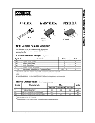
PN2222A
C
B
E
TO-92
MMBT2222A
C
B
E
SOT-23
Mark: 1P
PZT2222A
B
C
C
SOT-223
E
PN2222A/MMBT2222A/PZT2222A
2. Electrical Characteristics TA
= 25°C unless otherwise noted
Symbol Parameter Test Conditions Min Max Units
OFF CHARACTERISTICS
ONCHARACTERISTICS
SMALL SIGNAL CHARACTERISTICS
fT Current Gain - Bandwidth Product IC= 20 mA, VCE= 20 V, f= 100 MHz 300 MHz
Cobo Output Capacitance VCB = 10 V, IE = 0, f = 100 kHz 8.0 pF
Cibo Input Capacitance VEB = 0.5 V, IC = 0, f = 100 kHz 25 pF
rb’CC Collector Base Time Constant IC= 20 mA, VCB= 20 V, f= 31.8 MHz 150 pS
NF Noise Figure IC = 100 µA, VCE = 10 V,
RS = 1.0 kΩ, f = 1.0 kHz
4.0 dB
Re(hie) Real Part of Common-Emitter
High Frequency Input Impedance
IC = 20 mA, VCE = 20 V,
f = 300 MHz
60 Ω
SWITCHINGCHARACTERISTICS
*Pulse Test: Pulse Width ≤ 300 µs, Duty Cycle ≤ 2.0%
Spice Model
V(BR)CEO Collector-Emitter Breakdown Voltage* IC = 10 mA, IB = 0 40 V
V(BR)CBO Collector-Base Breakdown Voltage IC = 10 µA, IE = 0 75 V
V(BR)EBO Emitter-Base Breakdown Voltage IE = 10 µA, IC = 0 6.0 V
ICEX Collector Cutoff Current VCE = 60 V, VEB(OFF) = 3.0 V 10 nA
ICBO Collector Cutoff Current VCB = 60 V, IE = 0
VCB = 60 V, IE = 0, TA = 150°C
0.01
10
µA
µA
IEBO Emitter Cutoff Current VEB = 3.0 V, IC = 0 10 nA
IBL Base Cutoff Current VCE = 60 V, VEB(OFF) = 3.0 V 20 nA
hFE DC Current Gain IC = 0.1 mA, VCE = 10 V
IC = 1.0 mA, VCE = 10 V
IC = 10 mA, VCE = 10 V
IC = 10 mA, VCE = 10 V, TA = -55°C
IC = 150 mA, VCE = 10 V*
IC = 150 mA, VCE = 1.0 V*
IC = 500 mA, VCE = 10 V*
35
50
75
35
100
50
40
300
VCE(sat) Collector-Emitter Saturation
Voltage*
IC = 150 mA, IB = 15 mA
IC = 500 mA, IB = 50 mA
0.3
1.0
V
V
VBE(sat) Base-Emitter Saturation Voltage* IC = 150 mA, IB = 15 mA
IC = 500 mA, IB = 50 mA
0.6 1.2
2.0
V
V
td Delay Time VCC = 30 V, VBE(OFF) = 0.5 V, 10 ns
tr Rise Time IC = 150 mA, IB1 = 15 mA 25 ns
ts Storage Time VCC = 30 V, IC = 150 mA, 225 ns
tf Fall Time IB1 = IB2 = 15 mA 60 ns
NPN (Is=14.34f Xti=3 Eg=1.11 Vaf=74.03 Bf=255.9 Ne=1.307 Ise=14.34f Ikf=.2847 Xtb=1.5 Br=6.092 Nc=2 Isc=0
Ikr=0 Rc=1 Cjc=7.306p Mjc=.3416 Vjc=.75 Fc=.5 Cje=22.01p Mje=.377 Vje=.75 Tr=46.91n Tf=411.1p Itf=.6
Vtf=1.7 Xtf=3 Rb=10)
NPN General Purpose Amplifier
(continued)
PN2222A/MMBT2222A/PZT2222A
3. Typical Characteristics
Typical Pulsed Current Gain
vs Collector Current
0.1 0.3 1 3 10 30 100 300
0
100
200
300
400
500
I - COLLECTOR CURRENT (mA)
h-TYPICALPULSEDCURRENTGAIN
C
FE
125 °C
25 °C
- 40 °C
V = 5VCE
Collector-Emitter Saturation
Voltage vs Collector Current
1 10 100 500
0.1
0.2
0.3
0.4
I - COLLECTOR CURRENT (mA)
V-COLLECTOR-EMITTERVOLTAGE(V)CESAT
25 °C
C
β = 10
125 °C
- 40 °C
Base-Emitter Saturation
Voltage vs Collector Current
1 10 100 500
0.4
0.6
0.8
1
I - COLLECTOR CURRENT (mA)
V-BASE-EMITTERVOLTAGE(V)BESAT
C
β = 10
25 °C
125 °C
- 40 °C
Base-Emitter ON Voltage vs
Collector Current
0.1 1 10 25
0.2
0.4
0.6
0.8
1
I - COLLECTOR CURRENT (mA)
V-BASE-EMITTERONVOLTAGE(V)BE(ON)
C
V = 5VCE
25 °C
125 °C
- 40 °C
Collector-Cutoff Current
vs Ambient Temperature
25 50 75 100 125 150
0.1
1
10
100
500
T - AMBIENT TEMPERATURE ( C)
I-COLLECTORCURRENT(nA)
A
V = 40V
CB
CBO
°
Emitter Transition and Output
Capacitance vs Reverse Bias Voltage
0.1 1 10 100
4
8
12
16
20
REVERSE BIAS VOLTAGE (V)
CAPACITANCE(pF)
f = 1 MHz
C ob
C te
NPN General Purpose Amplifier
(continued)
PN2222A/MMBT2222A/PZT2222A
4. Typical Characteristics (continued)
Power Dissipation vs
Ambient Temperature
0 25 50 75 100 125 150
0
0.25
0.5
0.75
1
TEMPERATURE ( C)
P-POWERDISSIPATION(W)D
o
SOT-223
TO-92
SOT-23
Turn On and Turn Off Times
vs Collector Current
10 100 1000
0
80
160
240
320
400
I - COLLECTOR CURRENT (mA)
TIME(nS)
I = I =
t on
t off
B1
C
B2
I c
10
V = 25 Vcc
Switching Times
vs Collector Current
10 100 1000
0
80
160
240
320
400
I - COLLECTOR CURRENT (mA)
TIME(nS)
I = I =
t r
t s
B1
C
B2
I c
10
V = 25 Vcc
t f
t d
PN2222A/MMBT2222A/PZT2222A
NPN General Purpose Amplifier
(continued)
5. Typical Common Emitter Characteristics (f = 1.0kHz)
Common Emitter Characteristics
0 10 20 30 40 50 60
0
2
4
6
8
I - COLLECTOR CURRENT (mA)
CHAR.RELATIVETOVALUESATI=10mA
V = 10 VCE
C
C
T = 25 CA
o
hoe
hre
hfe
h ie
Common Emitter Characteristics
0 20 40 60 80 100
0
0.4
0.8
1.2
1.6
2
2.4
T - AMBIENT TEMPERATURE ( C)
CHAR.RELATIVETOVALUESATT=25C
V = 10 VCE
A
A
I = 10 mAC
hoe
hre
hfe
hie
o
o
Common Emitter Characteristics
0 5 10 15 20 25 30 35
0.75
0.8
0.85
0.9
0.95
1
1.05
1.1
1.15
1.2
1.25
1.3
V - COLLECTOR VOLTAGE (V)
CHAR.RELATIVETOVALUESATV=10V
CE
CE
T = 25 CA
o
hoe
hre
hfe
h ie
I = 10 mAC
NPN General Purpose Amplifier
(continued)
PN2222A/MMBT2222A/PZT2222A
6. Test Circuits
30V
1.0 KΩΩΩΩΩ
16V
0
≤≤≤≤≤ 200ns
≤≤≤≤≤ 200ns
500 ΩΩΩΩΩ
200 ΩΩΩΩΩ
50 ΩΩΩΩΩ
37 ΩΩΩΩΩ
- 1.5 V
1.0 KΩΩΩΩΩ
6.0V
0
30V
FIGURE 2: Saturated Turn-Off Switching Time
FIGURE 1: Saturated Turn-On Switching Time
1k
PN2222A/MMBT2222A/PZT2222A
NPN General Purpose Amplifier
(continued)
NOTE: BVEBO
= 5.0 V
8. TO-92 Tape and Reel Data, continued
September 1999, Rev. B
TO-92 Reeling Style
Configuration: Figure 2.0
Style “A”, D26Z, D70Z (s/h)
Machine Option “A” (H)
Style “E”, D27Z, D71Z (s/h)
Machine Option “E” (J)
FIRST WIRE OFF IS EMITTER
ADHESIVE TAPE IS ON THE TOP SIDE
FLAT OF TRANSISTOR IS ON BOTTOM
ORDER STYLE
D75Z (P)
FIRST WIRE OFF IS COLLECTOR
ADHESIVE TAPE IS ON THE TOP SIDE
FLAT OF TRANSISTOR IS ON TOP
ORDER STYLE
D74Z (M)
TO-92 Radial Ammo Packaging
Configuration: Figure 3.0
FIRST WIRE OFF IS EMITTER (ON PKG. 92)
ADHESIVE TAPE IS ON BOTTOM SIDE
FLAT OF TRANSISTOR IS ON BOTTOM
FIRST WIRE OFF IS COLLECTOR (ON PKG. 92)
ADHESIVE TAPE IS ON BOTTOM SIDE
FLAT OF TRANSISTOR IS ON TOP
9. ITEM DESCRIPTION
Base of Package to Lead Bend
Component Height
Lead Clinch Height
Component Base Height
Component Alignment ( side/side )
Component Alignment ( front/back )
Component Pitch
Feed Hole Pitch
Hole Center to First Lead
Hole Center to Component Center
Lead Spread
Lead Thickness
Cut Lead Length
Taped Lead Length
Taped Lead Thickness
Carrier Tape Thickness
Carrier Tape Width
Hold - down Tape Width
Hold - down Tape position
Feed Hole Position
Sprocket Hole Diameter
Lead Spring Out
SYMBOL
b
Ha
HO
H1
Pd
Hd
P
PO
P1
P2
F1/F2
d
L
L1
t
t1
W
WO
W1
W2
DO
S
DIMENSION
0.098 (max)
0.928 (+/- 0.025)
0.630 (+/- 0.020)
0.748 (+/- 0.020)
0.040 (max)
0.031 (max)
0.500 (+/- 0.020)
0.500 (+/- 0.008)
0.150 (+0.009, -0.010)
0.247 (+/- 0.007)
0.104 (+/- 0 .010)
0.018 (+0.002, -0.003)
0.429 (max)
0.209 (+0.051, -0.052)
0.032 (+/- 0.006)
0.021 (+/- 0.006)
0.708 (+0.020, -0.019)
0.236 (+/- 0.012)
0.035 (max)
0.360 (+/- 0.025)
0.157 (+0.008, -0.007)
0.004 (max)
Note : All dimensions are in inches.
ITEM DESCRIPTION SYSMBOL MINIMUM MAXIMUM
Reel Diameter D1 13.975 14.025
Arbor Hole Diameter (Standard) D2 1.160 1.200
(Small Hole) D2 0.650 0.700
Core Diameter D3 3.100 3.300
Hub Recess Inner Diameter D4 2.700 3.100
Hub Recess Depth W1 0.370 0.570
Flange to Flange Inner Width W2 1.630 1.690
Hub to Hub Center Width W3 2.090
Note: All dimensions are inches
TO-92 Tape and Reel Taping
Dimension Configuration: Figure 4.0
Ha
H1 HO
PO
P2
P1 F1
DO
P Pd
b
d
L1
L
S
WO
W2
W
t
t1
Hd
W1
TO-92 Reel
Configuration: Figure 5.0
User Direction of Feed
SEN SITIVE D EVICES
ELECTROSTATIC
D1
D3
Customized Label
W2
W1
W3
F63TNR Label
D4
D2
TO-92 Tape and Reel Data, continued
July 1999, Rev. A
12. Dimensions are in millimeter
Pkg type A0 B0 W D0 D1 E1 E2 F P1 P0 K0 T Wc Tc
SOT-23
(8mm)
3.15
+/-0.10
2.77
+/-0.10
8.0
+/-0.3
1.55
+/-0.05
1.125
+/-0.125
1.75
+/-0.10
6.25
min
3.50
+/-0.05
4.0
+/-0.1
4.0
+/-0.1
1.30
+/-0.10
0.228
+/-0.013
5.2
+/-0.3
0.06
+/-0.02
Dimensions are in inches and millimeters
Tape Size
Reel
Option
Dim A Dim B Dim C Dim D Dim N Dim W1 Dim W2 Dim W3 (LSL-USL)
8mm 7" Dia
7.00
177.8
0.059
1.5
512 +0.020/-0.008
13 +0.5/-0.2
0.795
20.2
2.165
55
0.331 +0.059/-0.000
8.4 +1.5/0
0.567
14.4
0.311 – 0.429
7.9 – 10.9
8mm 13" Dia
13.00
330
0.059
1.5
512 +0.020/-0.008
13 +0.5/-0.2
0.795
20.2
4.00
100
0.331 +0.059/-0.000
8.4 +1.5/0
0.567
14.4
0.311 – 0.429
7.9 – 10.9
See detail AA
Dim A
max
13" Diameter Option
7"Diameter Option
Dim A
Max
See detail AA
W3
W2 max Measured at Hub
W1 Measured at Hub
Dim N
Dim D
min
Dim C
B Min
DETAIL AA
Notes: A0, B0, and K0 dimensions are determined with respect to the EIA/Jedec RS-481
rotational and lateral movement requirements (see sketches A, B, and C).
20 deg maximum component rotation
0.5mm
maximum
0.5mm
maximum
Sketch C (Top View)
Component lateral movement
Typical
component
cavity
center line
20 deg maximum
Typical
component
center line
B0
A0
Sketch B (Top View)
Component Rotation
Sketch A (Side or Front Sectional View)
Component Rotation
User Direction of Feed
SOT-23 Embossed Carrier Tape
Configuration: Figure 3.0
SOT-23 Reel Configuration: Figure 4.0
P1 A0
D1
F W
E1
E2
Tc
Wc
K0
T
B0
D0P0 P2
SOT-23 Tape and Reel Data, continued
September 1999, Rev. C
15. Dimensions are in millimeter
Pkg type A0 B0 W D0 D1 E1 E2 F P1 P0 K0 T Wc Tc
SOT-223
(12mm)
6.83
+/-0.10
7.42
+/-0.10
12.0
+/-0.3
1.55
+/-0.05
1.50
+/-0.10
1.75
+/-0.10
10.25
min
5.50
+/-0.05
8.0
+/-0.1
4.0
+/-0.1
1.88
+/-0.10
0.292
+/-
0.0130
9.5
+/-0.025
0.06
+/-0.02
P1A0 D1
P0
F
W
E1
D0
E2
B0
Tc
Wc
K0
T
Dimensions are in inches and millimeters
Tape Size
Reel
Option
Dim A Dim B Dim C Dim D Dim N Dim W1 Dim W2 Dim W3 (LSL-USL)
12mm 7" Dia
7.00
177.8
0.059
1.5
512 +0.020/-0.008
13 +0.5/-0.2
0.795
20.2
5.906
150
0.488 +0.078/-0.000
12.4 +2/0
0.724
18.4
0.469 – 0.606
11.9 – 15.4
12mm 13" Dia
13.00
330
0.059
1.5
512 +0.020/-0.008
13 +0.5/-0.2
0.795
20.2
7.00
178
0.488 +0.078/-0.000
12.4 +2/0
0.724
18.4
0.469 – 0.606
11.9 – 15.4
See detail AA
Dim A
max
13" Diameter Option
7"Diameter Option
Dim A
Max
See detail AA
W3
W2 max Measured at Hub
W1 Measured at Hub
Dim N
Dim D
min
Dim C
B Min
DETAIL AA
Notes: A0, B0, and K0 dimensions are determined with respect to the EIA/Jedec RS-481
rotational and lateral movement requirements (see sketches A, B, and C).
20 deg maximum component rotation
0.5mm
maximum
0.5mm
maximum
Sketch C (Top View)
Component lateral movement
Typical
component
cavity
center line
20 deg maximum
Typical
component
center line
B0
A0
Sketch B (Top View)
Component Rotation
Sketch A (Side or Front Sectional View)
Component Rotation
User Direction of Feed
SOT-223 Embossed Carrier Tape
Configuration: Figure 3.0
SOT-223 Reel Configuration: Figure 4.0
SOT-223 Tape and Reel Data, continued
July 1999, Rev. B
17. TRADEMARKS
The following are registered and unregistered trademarks Fairchild Semiconductor owns or is authorized to use and is
not intended to be an exhaustive list of all such trademarks.
LIFE SUPPORT POLICY
FAIRCHILD’S PRODUCTS ARE NOT AUTHORIZED FOR USE AS CRITICAL COMPONENTS IN LIFE SUPPORT
DEVICESORSYSTEMSWITHOUTTHEEXPRESSWRITTENAPPROVALOFFAIRCHILDSEMICONDUCTORCORPORATION.
As used herein:
1. Life support devices or systems are devices or
systems which, (a) are intended for surgical implant into
the body, or (b) support or sustain life, or (c) whose
failure to perform when properly used in accordance
with instructions for use provided in the labeling, can be
reasonably expected to result in significant injury to the
user.
2. A critical component is any component of a life
support device or system whose failure to perform can
be reasonably expected to cause the failure of the life
support device or system, or to affect its safety or
effectiveness.
PRODUCT STATUS DEFINITIONS
Definition of Terms
Datasheet Identification Product Status Definition
Advance Information
Preliminary
No Identification Needed
Obsolete
This datasheet contains the design specifications for
product development. Specifications may change in
any manner without notice.
This datasheet contains preliminary data, and
supplementary data will be published at a later date.
Fairchild Semiconductor reserves the right to make
changes at any time without notice in order to improve
design.
This datasheet contains final specifications. Fairchild
Semiconductor reserves the right to make changes at
any time without notice in order to improve design.
This datasheet contains specifications on a product
that has been discontinued by Fairchild semiconductor.
The datasheet is printed for reference information only.
Formative or
In Design
First Production
Full Production
Not In Production
DISCLAIMER
FAIRCHILD SEMICONDUCTOR RESERVES THE RIGHT TO MAKE CHANGES WITHOUT FURTHER
NOTICE TOANY PRODUCTS HEREIN TO IMPROVE RELIABILITY, FUNCTION OR DESIGN. FAIRCHILD
DOES NOTASSUMEANY LIABILITYARISING OUT OF THE APPLICATION OR USE OFANY PRODUCT
OR CIRCUIT DESCRIBED HEREIN; NEITHER DOES IT CONVEY ANY LICENSE UNDER ITS PATENT
RIGHTS, NOR THE RIGHTS OF OTHERS.
PowerTrench
QFET™
QS™
QT Optoelectronics™
Quiet Series™
SILENT SWITCHER
SMART START™
SuperSOT™-3
SuperSOT™-6
SuperSOT™-8
FASTr™
GlobalOptoisolator™
GTO™
HiSeC™
ISOPLANAR™
MICROWIRE™
OPTOLOGIC™
OPTOPLANAR™
PACMAN™
POP™
Rev. G
ACEx™
Bottomless™
CoolFET™
CROSSVOLT™
DOME™
E2
CMOSTM
EnSignaTM
FACT™
FACT Quiet Series™
FAST
SyncFET™
TinyLogic™
UHC™
VCX™