
Recommended
Recommended
More Related Content
Similar to Original IGBT N-CHANNEL IRG7IC28U IRG71C28U G7IC28U G71C28U 71C28 225A 600V TO-220 New IR
Similar to Original IGBT N-CHANNEL IRG7IC28U IRG71C28U G7IC28U G71C28U 71C28 225A 600V TO-220 New IR (20)
More from authelectroniccom
More from authelectroniccom (20)
Recently uploaded
Recently uploaded (20)
Original IGBT N-CHANNEL IRG7IC28U IRG71C28U G7IC28U G71C28U 71C28 225A 600V TO-220 New IR
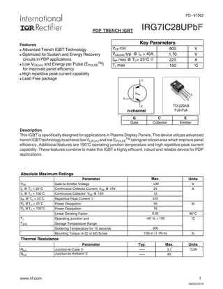
- 1. www.irf.com 1 09/02/2010 IRG7IC28UPbF Description This IGBT is specifically designed for applications in Plasma Display Panels. This device utilizes advanced trenchIGBTtechnologytoachievelowVCE(on) andlowEPULSE TM ratingpersiliconareawhichimprovepanel efficiency. Additional features are 150°C operating junction temperature and high repetitive peak current capability. These features combine to make this IGBT a highly efficient, robust and reliable device for PDP applications. Features l Advanced Trench IGBT Technology l Optimized for Sustain and Energy Recovery circuits in PDP applications l Low VCE(on) and Energy per Pulse (EPULSE TM) for improved panel efficiency l High repetitive peak current capability l Lead Free package PDP TRENCH IGBT E C G n-channel G C E Gate Collector Emitter TO-220AB Full-Pak G C E PD - 97562 Absolute Maximum Ratings Parameter Units VGE Gate-to-Emitter Voltage V IC @ TC = 25°C Continuous Collector Current, VGE @ 15V A IC @ TC = 100°C Continuous Collector, VGE @ 15V IRP @ TC = 25°C Repetitive Peak Current c PD @TC = 25°C Power Dissipation W PD @TC = 100°C Power Dissipation Linear Derating Factor W/°C TJ Operating Junction and °C TSTG Storage Temperature Range Soldering Temperature for 10 seconds Mounting Torque, 6-32 or M3 Screw N Thermal Resistance Parameter Typ. Max. Units RθJC Junction-to-Case d ––– 3.1 °C/W RθJA Junction-to-Ambient d ––– 65 Max. 12 225 25 ±30 300 -40 to + 150 10lbxin (1.1Nxm) 40 16 0.32 VCE min 600 V VCE(ON) typ. @ IC = 40A 1.70 V IRP max @ TC= 25°C c 225 A TJ max 150 °C Key Parameters
- 2. IRG7IC28UPbF 2 www.irf.com Notes: Half sine wave with duty cycle <= 0.02, ton=1.0µsec. ‚ Rθ is measured at TJ of approximately 90°C. ƒ Pulse width ≤ 400µs; duty cycle ≤ 2%. Electrical Characteristics @ TJ = 25°C (unless otherwise specified) Parameter Min. Typ. Max. Units BVCES Collector-to-Emitter Breakdown Voltage 600 ––– ––– V V(BR)ECS Emitter-to-Collector Breakdown Voltagee 15 ––– ––– V ∆ΒVCES/∆TJ Breakdown Voltage Temp. Coefficient ––– 0.57 ––– V/°C ––– 1.25 ––– ––– 1.42 ––– 1.70 1.95 V ––– 1.96 ––– ––– 2.97 ––– ––– 1.75 ––– VGE(th) Gate Threshold Voltage 2.2 ––– 4.7 V ∆VGE(th)/∆TJ Gate Threshold Voltage Coefficient ––– -11 ––– mV/°C ICES Collector-to-Emitter Leakage Current ––– 0.5 20 ––– 30 ––– µA ––– 90 ––– 305 ––– IGES Gate-to-Emitter Forward Leakage ––– ––– 100 nA Gate-to-Emitter Reverse Leakage ––– ––– -100 gfe Forward Transconductance ––– 55 ––– S Qg Total Gate Charge ––– 70 ––– nC Qgc Gate-to-Collector Charge ––– 25 ––– td(on) Turn-On delay time ––– 30 ––– IC = 40A, VCC = 400V tr Rise time ––– 35 ––– ns RG = 22Ω, L=100µH td(off) Turn-Off delay time ––– 260 ––– TJ = 25°C tf Fall time ––– 145 ––– td(on) Turn-On delay time ––– 25 ––– IC = 40A, VCC = 400V tr Rise time ––– 40 ––– ns RG = 22Ω, L=100µH td(off) Turn-Off delay time ––– 280 ––– TJ = 150°C tf Fall time ––– 320 ––– tst Shoot Through Blocking Time 100 ––– ––– ns EPULSE Energy per Pulse µJ Human Body Model Machine Model Cies Input Capacitance ––– 1880 ––– Coes Output Capacitance ––– 75 ––– pF Cres Reverse Transfer Capacitance ––– 45 ––– LC Internal Collector Inductance ––– 4.5 ––– Between lead, nH 6mm (0.25in.) LE Internal Emitter Inductance ––– 7.5 ––– from package VGE = 15V, ICE = 160A e Static Collector-to-Emitter VoltageVCE(on) VGE = 15V, ICE = 40A, TJ = 150°C e VGE = 15V, ICE = 40A e ––– 930 ––– VCE = 25V, ICE = 40A VCE = 400V, IC = 40A, VGE = 15Ve VCC = 240V, RG= 5.1Ω, TJ = 25°C ––– 770 ––– VCC = 240V, VGE = 15V, RG= 5.1Ω VCE = VGE, ICE = 250µA VCE = 600V, VGE = 0V VCE = 600V, VGE = 0V, TJ = 150°C VGE = 30V VGE = -30V VCE = 600V, VGE = 0V, TJ = 100°C ƒ = 1.0MHz and center of die contact VCE = 600V, VGE = 0V, TJ = 125°C L = 220nH, C= 0.40µF, VGE = 15V L = 220nH, C= 0.40µF, VGE = 15V VCC = 240V, RG= 5.1Ω, TJ = 100°C Conditions VGE = 0V, ICE = 1.0mA Reference to 25°C, ICE = 1.0mA VGE = 15V, ICE = 70A e VGE = 15V, ICE = 12A e VGE = 15V, ICE = 24A e VGE = 0V, ICE = 1.0A ESD Class H1C (2000V) (Per JEDEC standard JESD22-A114) Class M4 (425V) (Per EIA/JEDEC standard EIA/JESD22-A115) VCE = 30V VGE = 0V
- 3. IRG7IC28UPbF www.irf.com 3 Fig 1. Typical Output Characteristics @ 25°C Fig 3. Typical Output Characteristics @ 125°C Fig 4. Typical Output Characteristics @ 150°C Fig 2. Typical Output Characteristics @ 75°C Fig 5. Typical Transfer Characteristics Fig 6. VCE(ON) vs. Gate Voltage 0 2 4 6 8 10 VCE (V) 0 25 50 75 100 125 150 175 200 ICE(A) VGE = 18V VGE = 15V VGE = 12V VGE = 10V VGE = 8.0V VGE = 6.0V 0 2 4 6 8 10 VCE (V) 0 25 50 75 100 125 150 175 200 ICE(A) VGE = 18V VGE = 15V VGE = 12V VGE = 10V VGE = 8.0V VGE = 6.0V 0 2 4 6 8 10 12 14 VCE (V) 0 25 50 75 100 125 150 175 200 ICE(A) VGE = 18V VGE = 15V VGE = 12V VGE = 10V VGE = 8.0V VGE = 6.0V 0 2 4 6 8 10 12 14 VCE (V) 0 25 50 75 100 125 150 175 200 ICE(A) VGE = 18V VGE = 15V VGE = 12V VGE = 10V VGE = 8.0V VGE = 6.0V 2 4 6 8 10 VGE, Gate-to-Emitter Voltage (V) 0 25 50 75 100 125 150 175 200 ICE,Collector-to-EmitterCurrent(A) TJ = 25°C TJ = 150°C 0 5 10 15 20 VGE, Voltage Gate-to-Emitter (V) 1.2 1.4 1.6 1.8 2.0 VCE,VoltageCollector-to-Emitter(V) TJ = 25°C TJ = 150°C IC = 20A
- 4. IRG7IC28UPbF 4 www.irf.com Fig 7. Maximum Collector Current vs. Case Temperature Fig 8. Typical Repetitive Peak Current vs. Case Temperature Fig 10. Typical EPULSE vs. Collector-to-Emitter VoltageFig 9. Typical EPULSE vs. Collector Current Fig 11. EPULSE vs. Temperature Fig 12. Forrward Bias Safe Operating Area 25 50 75 100 125 150 TC (°C) 0 5 10 15 20 25IC(A) 25 50 75 100 125 150 Case Temperature (°C) 0 50 100 150 200 250 RepetitivePeakCurrent(A) ton= 2µs Duty cycle <= 0.05 Half Sine Wave 160 170 180 190 200 210 220 230 240 IC, Peak Collector Current (A) 450 500 550 600 650 700 750 800 850 900 950 EnergyperPulse(µJ) VCC= 240V L = 220nH C = variable 100°C 25°C 200 205 210 215 220 225 230 235 240 VCE, Collector-to-Emitter Voltage (V) 450 500 550 600 650 700 750 800 850 900 950 EnergyperPulse(µJ) L = 220nH C = 0.4µF 100°C 25°C 20 40 60 80 100 120 140 160 TJ, Temperature (ºC) 400 500 600 700 800 900 1000 1100 EnergyperPulse(µJ) VCC= 240V L = 220nH t = 1µs half sine C= 0.4µF C= 0.3µF C= 0.2µF 1.0 10 100 1000 VCE (V) 1 10 100 1000 IC(A) 1msec 10µsec 100µsec Tc = 25°C Tj = 150°C Single Pulse
- 5. IRG7IC28UPbF www.irf.com 5 Fig 13. Typical Capacitance vs. Collector-to-Emitter Voltage Fig 14. Typical Gate Charge vs. Gate-to-Emitter Voltage Fig 16. Maximum Effective Transient Thermal Impedance, Junction-to-Case Fig. 15 - Typ. Energy Loss vs. IC TJ = 150°C; L = 250µH; VCE = 400V, RG = 22Ω; VGE = 15V 0 100 200 300 400 500 VCE, Collector-toEmitter-Voltage(V) 10 100 1000 10000 100000Capacitance(pF) Cies Coes Cres VGS = 0V, f = 1 MHZ Cies = Cge + Cgd, C ce SHORTED Cres = Cgc Coes = Cce + Cgc 0 10 20 30 40 50 60 70 80 Q G, Total Gate Charge (nC) 0 2 4 6 8 10 12 14 16 VGE,Gate-to-EmitterVoltage(V) VCES = 120V VCES = 300V VCES = 400V IC = 40A 0 10 20 30 40 50 60 70 80 90 IC (A) 0 1000 2000 3000 4000 5000 6000 Energy(µJ) EOFF EON 1E-006 1E-005 0.0001 0.001 0.01 0.1 1 10 100 t1 , Rectangular Pulse Duration (sec) 0.001 0.01 0.1 1 10 ThermalResponse(ZthJC) 0.20 0.10 D = 0.50 0.02 0.01 0.05 SINGLE PULSE ( THERMAL RESPONSE ) Notes: 1. Duty Factor D = t1/t2 2. Peak Tj = P dm x Zthjc + Tc τJ τJ τ1 τ1 τ2 τ2 τ3 τ3 R1 R1 R2 R2 R3 R3 Ci i/Ri Ci= τi/Ri τ τC τ4 τ4 R4 R4 Ri (°C/W) τi (sec) 0.19973 0.000268 0.38341 0.002261 1.17794 0.154543 1.36892 2.511
- 6. IRG7IC28UPbF 6 www.irf.com Fig 16a. tst and EPULSE Test Circuit Fig 16b. tst Test Waveforms Fig 16c. EPULSE Test Waveforms 1K VCC DUT 0 L Fig. 17 - Gate Charge Circuit (turn-off) DRIVER DUT L C VCC RG RG B A Ipulse Energy VCE IC Current PULSEA PULSEB tST
- 7. IRG7IC28UPbF www.irf.com 7 TO-220AB Full-Pak package is not recommended for Surface Mount Application. Data and specifications subject to change without notice. This product has been designed for the Industrial market. Qualification Standards can be found on IR’s Web site. IR WORLD HEADQUARTERS: 233 Kansas St., El Segundo, California 90245, USA Tel: (310) 252-7105 TAC Fax: (310) 252-7903 Visit us at www.irf.com for sales contact information.09/2010 The specifications set forth in this data sheet are the sole and exclusive specifications applicable to the identified product, and no specifications or features are implied whether by industry custom, sampling or otherwise. We qualify our products in accordance with our internal practices and procedures, which by their nature do not include qualification to all possible or even all widely used applications. Without limitation, we have not qualified our product for medical use or applications involving hi-reliability applications. Customers are encouraged to and responsible for qualifying product to their own use and their own application environments, especially where particular features are critical to operational performance or safety. Please contact your IR representative if you have specific design or use requirements or for further information. Note: For the most current drawing please refer to IR website at http://www.irf.com/package/ TO-220AB Full-Pak Package Outline Dimensions are shown in millimeters (inches) TO-220AB Full-Pak Part Marking Information GPBPDIÃUC@Ã6TT@H7G`ÃGDI@ÃÅFÅ 6TT@H7G@9ÃPIÃXXÃ!#Ã! @Y6HQG@) GPUÃ8P9@Ã#! UCDTÃDTÃ6IÃDSAD'#Bà XDUCÃ6TT@H7G`à Q6SUÃIVH7@S DIU@SI6UDPI6G S@8UDAD@S !#F DSAD'#B I‚‡r)ÃÅQÅÃvÃh††r€iy’Ãyvr†v‡v‚ vqvph‡r†ÃÅGrhqA…rrÅ GDI@ÃF X@@FÃ!# `@6Sà Ã2Ã! 96U@Ã8P9@ GPUÃ8P9@ 6TT@H7G` Ã#ÃÃÃÃÃÃÃÃÃ!