
Recommended
Recommended
More Related Content
What's hot
What's hot (20)
Similar to Original IGBT IRG4BC20KD G4BC20KD 600V 9A TO-220 New
Similar to Original IGBT IRG4BC20KD G4BC20KD 600V 9A TO-220 New (14)
More from AUTHELECTRONIC
More from AUTHELECTRONIC (20)
Recently uploaded
Recently uploaded (20)
Original IGBT IRG4BC20KD G4BC20KD 600V 9A TO-220 New
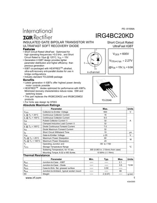
- 1. Parameter Max. Units VCES Collector-to-Emitter Voltage 600 V IC @ TC = 25°C Continuous Collector Current 16 IC @ TC = 100°C Continuous Collector Current 9.0 ICM Pulsed Collector Current Q 32 A ILM Clamped Inductive Load Current R 32 IF @ TC = 100°C Diode Continuous Forward Current 7.0 IFM Diode Maximum Forward Current 32 tsc Short Circuit Withstand Time 10 µs VGE Gate-to-Emitter Voltage ± 20 V PD @ TC = 25°C Maximum Power Dissipation 60 PD @ TC = 100°C Maximum Power Dissipation 24 TJ Operating Junction and -55 to +150 TSTG Storage Temperature Range °C Soldering Temperature, for 10 sec. 300 (0.063 in. (1.6mm) from case) Mounting Torque, 6-32 or M3 Screw. 10 lbf•in (1.1 N•m) IRG4BC20KD INSULATED GATE BIPOLAR TRANSISTOR WITH ULTRAFAST SOFT RECOVERY DIODE FeaturesFeaturesFeaturesFeaturesFeatures E G n-channel C VCES = 600V VCE(on) typ. = 2.27V @VGE = 15V, IC = 9.0A Short Circuit Rated UltraFast IGBT 4/24/2000 • Short Circuit Rated UltraFast: Optimized for high operating frequencies >5.0 kHz , and Short Circuit Rated to 10µs @ 125°C, VGE = 15V • Generation 4 IGBT design provides tighter parameter distribution and higher efficiency than previous generation • IGBT co-packaged with HEXFREDTM ultrafast, ultra-soft-recovery anti-parallel diodes for use in bridge configurations • Industry standard TO-220AB package Benefits PD -91599A Parameter Min. Typ. Max. Units RθJC Junction-to-Case - IGBT ––– ––– 2.1 RθJC Junction-to-Case - Diode ––– ––– 3.5 °C/W RθCS Case-to-Sink, flat, greased surface ––– 0.50 ––– RθJA Junction-to-Ambient, typical socket mount ––– ––– 80 Wt Weight ––– 2 (0.07) ––– g (oz) Thermal Resistance Absolute Maximum Ratings W TO-220AB • Latest generation 4 IGBTs offer highest power density motor controls possible • HEXFREDTM diodes optimized for performance with IGBTs. Minimized recovery characteristics reduce noise, EMI and switching losses • This part replaces the IRGBC20KD2 and IRGBC20MD2 products • For hints see design tip 97003 www.irf.com 1
- 2. IRG4BC20KD 2 www.irf.com Parameter Min. Typ. Max. Units Conditions Qg Total Gate Charge (turn-on) — 34 51 IC = 9.0A Qge Gate - Emitter Charge (turn-on) — 4.9 7.4 nC VCC = 400V See Fig.8 Qgc Gate - Collector Charge (turn-on) — 14 21 VGE = 15V td(on) Turn-On Delay Time — 54 — tr Rise Time — 34 — TJ = 25°C td(off) Turn-Off Delay Time — 180 270 IC = 9.0A, VCC = 480V tf Fall Time — 72 110 VGE = 15V, RG = 50Ω Eon Turn-On Switching Loss — 0.34 — Energy losses include "tail" Eoff Turn-Off Switching Loss — 0.30 — mJ and diode reverse recovery Ets Total Switching Loss — 0.64 0.96 See Fig. 9,10,14 tsc Short Circuit Withstand Time 10 — — µs VCC = 360V, TJ = 125°C VGE = 15V, RG = 50Ω , VCPK < 500V td(on) Turn-On Delay Time — 51 — TJ = 150°C, See Fig. 11,14 tr Rise Time — 37 — IC = 9.0A, VCC = 480V td(off) Turn-Off Delay Time — 220 — VGE = 15V, RG = 50Ω tf Fall Time — 160 — Energy losses include "tail" Ets Total Switching Loss — 0.85 — mJ and diode reverse recovery LE Internal Emitter Inductance — 7.5 — nH Measured 5mm from package Cies Input Capacitance — 450 — VGE = 0V Coes Output Capacitance — 61 — pF VCC = 30V See Fig. 7 Cres Reverse Transfer Capacitance — 14 — ƒ = 1.0MHz trr Diode Reverse Recovery Time — 37 55 ns TJ = 25°C See Fig. — 55 90 TJ = 125°C 14 IF = 8.0A Irr Diode Peak Reverse Recovery Current — 3.5 5.0 A TJ = 25°C See Fig. — 4.5 8.0 TJ = 125°C 15 VR = 200V Qrr Diode Reverse Recovery Charge — 65 138 nC TJ = 25°C See Fig. — 124 360 TJ = 125°C 16 di/dt = 200Aµs di(rec)M/dt Diode Peak Rate of Fall of Recovery — 240 — A/µs TJ = 25°C See Fig. During tb — 210 — TJ = 125°C 17 Parameter Min. Typ. Max. Units Conditions V(BR)CES Collector-to-Emitter Breakdown VoltageS 600 — — V VGE = 0V, IC = 250µA ∆V(BR)CES/∆TJ Temperature Coeff. of Breakdown Voltage — 0.49 — V/°C VGE = 0V, IC = 1.0mA VCE(on) Collector-to-Emitter Saturation Voltage — 2.27 2.8 IC = 9.0A VGE = 15V — 3.01 — V IC = 16A See Fig. 2, 5 — 2.43 — IC = 9.0A, TJ = 150°C VGE(th) Gate Threshold Voltage 3.0 — 6.0 VCE = VGE, IC = 250µA ∆VGE(th)/∆TJ Temperature Coeff. of Threshold Voltage — -10 — mV/°C VCE = VGE, IC = 250µA gfe Forward Transconductance T 2.9 4.3 — S VCE = 100V, IC = 9.0A ICES Zero Gate Voltage Collector Current — — 250 µA VGE = 0V, VCE = 600V — — 1000 VGE = 0V, VCE = 600V, TJ = 150°C VFM Diode Forward Voltage Drop — 1.4 1.7 V IC = 8.0A See Fig. 13 — 1.3 1.6 IC = 8.0A, TJ = 150°C IGES Gate-to-Emitter Leakage Current — — ±100 nA VGE = ±20V Switching Characteristics @ TJ = 25°C (unless otherwise specified) Electrical Characteristics @ TJ = 25°C (unless otherwise specified) ns ns
- 3. IRG4BC20KD www.irf.com 3 0.1 1 10 100 0 2 4 6 8 10 f, Frequency (KHz) LOADCURRENT(A) Fig. 1 - Typical Load Current vs. Frequency (Load Current = IRMS of fundamental) For both: Duty cycle: 50% T = 125°C T = 90°C Gate drive as specified sink J Power Dissipation = W 60% of rated voltage I Ideal diodes Square wave: 13 Fig. 2 - Typical Output Characteristics Fig. 3 - Typical Transfer Characteristics 1 10 100 1 10 V , Collector-to-Emitter Voltage (V) I,Collector-to-EmitterCurrent(A) CE C V = 15V 20µs PULSE WIDTH GE T = 25 CJ o T = 150 CJ o 1 10 100 5 10 15 20 V , Gate-to-Emitter Voltage (V) I,Collector-to-EmitterCurrent(A) GE C V = 50V 5µs PULSE WIDTH CC T = 25 CJ o T = 150 CJ o
- 4. IRG4BC20KD 4 www.irf.com Fig. 6 - Maximum Effective Transient Thermal Impedance, Junction-to-Case Fig. 5 - Typical Collector-to-Emitter Voltage vs. Junction Temperature Fig. 4 - Maximum Collector Current vs. Case Temperature -60 -40 -20 0 20 40 60 80 100 120 140 160 1.0 2.0 3.0 4.0 5.0 T , Junction Temperature ( C) V,Collector-to-EmitterVoltage(V) J ° CE V = 15V 80 us PULSE WIDTH GE I = A4.5C I = A9C I = A18C 25 50 75 100 125 150 0 5 10 15 20 T , Case Temperature ( C) MaximumDCCollectorCurrent(A) C ° 0.01 0.1 1 10 0.00001 0.0001 0.001 0.01 0.1 1 Notes: 1. Duty factor D = t / t 2. Peak T = P x Z + T 1 2 J DM thJC C P t t DM 1 2 t , Rectangular Pulse Duration (sec) ThermalResponse(Z) 1 thJC 0.01 0.02 0.05 0.10 0.20 D = 0.50 SINGLE PULSE (THERMAL RESPONSE) 9.0A
- 5. IRG4BC20KD www.irf.com 5 0 10 20 30 40 50 0.5 0.6 0.7 0.8 R , Gate Resistance (Ohm) TotalSwitchingLosses(mJ) G V = 480V V = 15V T = 25 C I = 9.0A CC GE J C ° Fig. 7 - Typical Capacitance vs. Collector-to-Emitter Voltage Fig. 8 - Typical Gate Charge vs. Gate-to-Emitter Voltage Fig. 9 - Typical Switching Losses vs. Gate Resistance Fig. 10 - Typical Switching Losses vs. Junction Temperature 0 10 20 30 40 0 4 8 12 16 20 Q , Total Gate Charge (nC) V,Gate-to-EmitterVoltage(V) G GE V = 400V I = 9.0A CC C 1 10 100 0 200 400 600 800 V , Collector-to-Emitter Voltage (V) C,Capacitance(pF) CE V C C C = = = = 0V, C C C f = 1MHz + C + C C SHORTED GE ies ge gc , ce res gc oes ce gc Cies Coes Cres RG , Gate Resistance ( Ω ) -60 -40 -20 0 20 40 60 80 100 120 140 160 0.1 1 10 T , Junction Temperature ( C ) TotalSwitchingLosses(mJ) J ° R = Ohm V = 15V V = 480V G GE CC I = A18C I = A9C I = A4.5C 50Ω 9.0A
- 6. IRG4BC20KD 6 www.irf.com Fig. 11 - Typical Switching Losses vs. Collector-to-Emitter Current Fig. 12 - Turn-Off SOA 1 10 100 1 10 100 1000 V = 20V T = 125 C GE J o V , Collector-to-Emitter Voltage (V)I,Collector-to-EmitterCurrent(A) CEC SAFE OPERATING AREA Fig. 13 - Maximum Forward Voltage Drop vs. Instantaneous Forward Current 0.1 1 10 100 0.4 0.8 1.2 1.6 2.0 2.4 2.8 3.2 FM FInstantaneousForwardCurrent-I(A) Forward Voltage Drop - V (V) T = 150°C T = 125°C T = 25°C J J J 0 4 8 12 16 20 0.0 1.0 2.0 3.0 I , Collector-to-emitter Current (A) TotalSwitchingLosses(mJ) C R = Ohm T = 150 C V = 480V V = 15V G J CC GE ° 50Ω
- 7. IRG4BC20KD www.irf.com 7 Fig. 14 - Typical Reverse Recovery vs. dif/dt Fig. 15 - Typical Recovery Current vs. dif/dt Fig. 16 - Typical Stored Charge vs. dif/dt Fig. 17 - Typical di(rec)M/dt vs. dif/dt 0 100 200 300 400 500 100 1000 fdi /dt - (A/µs) RRQ-(nC) I = 16A I = 8.0A I = 4.0AF F F V = 200V T = 125°C T = 25°C R J J 100 1000 10000 100 1000 fdi /dt - (A/µs) di(rec)M/dt-(A/µs) I = 16A I = 8.0A I = 4.0A F F F V = 200V T = 125°C T = 25°C R J J 0 20 40 60 80 100 100 1000 fdi /dt - (A/µs) t-(ns)rr I = 16A I = 8.0A I = 4.0A F F F V = 200V T = 125°C T = 25°C R J J 1 10 100 100 1000 fdi /dt - (A/µs) I-(A)IRRM I = 16A I = 8.0A I = 4.0AF F F V = 200V T = 125°C T = 25°C R J J
- 8. IRG4BC20KD 8 www.irf.com Same type device as D.U.T. D.U.T. 430µF 80% of Vce Fig. 18a - Test Circuit for Measurement of ILM, Eon, Eoff(diode), trr, Qrr, Irr, td(on), tr, td(off), tf t1 Ic Vce t1 t2 90% Ic 10% Vce td(off) tf Ic 5% Ic t1+5µS Vce ic dt 90% Vge +Vge ∫Eoff = Fig. 18b - Test Waveforms for Circuit of Fig. 18a, Defining Eoff, td(off), tf ∫Vce ie dt t2 t1 5% Vce Ic IpkVcc 10% Ic Vce t1 t2 D UT VO LTAGE AN D CU RRE NT GATE VOLTA GE D .U .T. +Vg 10% +Vg 90% Ic trtd(on) DIO DE REVE RSE REC OVERY ENER GY tx E on = ∫Erec = t4 t3 Vd id dt t4t3 DIODE RE COV ERY W AVEFO RMS Ic V pk 10% Vcc Irr 10% Irr Vcc trr ∫Q rr = trr tx id dt Fig. 18c - Test Waveforms for Circuit of Fig. 18a, Defining Eon, td(on), tr Fig. 18d - Test Waveforms for Circuit of Fig. 18a, Defining Erec, trr, Qrr, Irr Vd Ic dt Vce Ic dt Ic dt Vce Ic dt
- 9. IRG4BC20KD www.irf.com 9 Vg GATE SIG NAL DEVICE U NDE R TEST CUR REN T D .U .T. VOLTAGE IN D.U.T. CUR REN T IN D1 t0 t1 t2 D.U.T. V *c 50V L 1000V 6000µF 100V Figure 19. Clamped Inductive Load Test Circuit Figure 20. Pulsed Collector Current Test Circuit RL= 480V 4 X IC @25°C 0 - 480V Figure 18e. Macro Waveforms for Figure 18a's Test Circuit
- 10. IRG4BC20KD 10 www.irf.com Notes: QRepetitiverating:VGE=20V;pulsewidthlimitedbymaximumjunctiontemperature (figure20) RVCC=80%(VCES),VGE=20V,L=10µH,RG=50Ω(figure19) SPulsewidth≤80µs;dutyfactor≤0.1%. TPulsewidth5.0µs,singleshot. Case Outline — TO-220AB 0.55 (.022) 0.46 (.018) 3 X 2.92 (.115) 2.64 (.104) 1.32 (.052) 1.22 (.048) - B - 4.69 (.185) 4.20 (.165) 3.78 (.149) 3.54 (.139) - A - 6.47 (.255) 6.10 (.240) 1.15 (.045) MIN 4.06 (.160) 3.55 (.140) 3 X 3.96 (.160) 3.55 (.140) 3 X 0.93 (.037) 0.69 (.027) 0.36 (.014) M B A M 10.54 (.415) 10.29 (.405)2.87 (.113) 2.62 (.103) 15.24 (.600) 14.84 (.584) 14.09 (.555) 13.47 (.530) 1.40 (.055) 1.15 (.045)3 X 2.54 (.100) 2X 1 2 3 4 CONFORMS TO JEDEC OUTLINE TO-220AB Dim ensions in M illim eters and (Inches) LEAD ASSIGNM ENT S 1 - GATE 2 - COLLE CTO R 3 - EM IT TER 4 - COLLE CTO R NO TES: 1 DIM ENSIONS T OLERANCING PER ANSI Y14.5M , 1982. 2 CO NTR OLLIN G DIM ENSION : INCH. 3 DIM ENSIONS ARE SHO W N M ILLIM ETER S (IN CHES ). 4 CO NFO RM S TO JEDEC OU TLINE T O-220AB. IR WORLD HEADQUARTERS: 233 Kansas St., El Segundo, California 90245, USA Tel: (310) 252-7105 IR EUROPEAN REGIONAL CENTRE: 439/445 Godstone Rd, Whyteleafe, Surrey CR3 OBL, UK Tel: ++ 44 (0)20 8645 8000 IR CANADA: 15 Lincoln Court, Brampton, Ontario L6T3Z2, Tel: (905) 453 2200 IR GERMANY: Saalburgstrasse 157, 61350 Bad Homburg Tel: ++ 49 (0) 6172 96590 IR ITALY: Via Liguria 49, 10071 Borgaro, Torino Tel: ++ 39 011 451 0111 IR JAPAN: KH Bldg., 2F, 30-4 Nishi-Ikebukuro 3-Chome, Toshima-Ku, Tokyo 171 Tel: 81 (0)3 3983 0086 IR SOUTHEAST ASIA: 1 Kim Seng Promenade, Great World City West Tower, 13-11, Singapore 237994 Tel: ++ 65 (0)838 4630 IR TAIWAN:16 Fl. Suite D. 207, Sec. 2, Tun Haw South Road, Taipei, 10673 Tel: 886-(0)2 2377 9936 Data and specifications subject to change without notice. 10/00
- 11. Note: For the most current drawings please refer to the IR website at: http://www.irf.com/package/