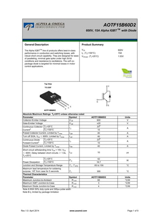
This document provides specifications for the AOTF15B60D2 600V, 15A Alpha IGBT module with an integrated diode. Key parameters include:
- Continuous collector current of 15A at 25°C and 23A at 100°C
- Collector-emitter saturation voltage of 1.53V at 25°C junction temperature
- Soft reverse recovery characteristics of the integrated diode targeted for low losses in motor control applications
The module is rated for 600V blocking voltage and features robust short circuit withstand capability with low conduction and switching losses.
Field-effect transistor amplifiers provide an excellent voltage gain with the added feature of high input impedance. They are also low-power-consumption configurations with good frequency range and minimal size and weight.
JFETs, depletion MOSFETs, and MESFETs can be used to design amplifiers having similar voltage gains.
The depletion MOSFET (MESFET) circuit, however, has a much higher input impedance than a similar JFET configuration.
In this configuration base is common for both input and output, input signal is applied between emitter and base terminals; and output is collected between collector and base terminals. Copy the link given below and paste it in new browser window to get more information on Common Emitter Configuration:- http://www.transtutors.com/homework-help/electrical-engineering/transistors/common-emitter-configuration.aspx
PN junction diode –structure, operation and V-I characteristics, diffusion and transient capacitance - Rectifiers – Half Wave and Full Wave Rectifier,– Display devices- LED, Laser diodes- Zener diodecharacteristics-Zener Reverse characteristics – Zener as regulator,TRANSISTORS, BJT, JFET, MOSFET- structure, operation, characteristics and Biasing UJT, Thyristor and IGBT Structure and characteristics,BJT small signal model – Analysis of CE, CB, CC amplifiers- Gain and frequency response –
MOSFET small signal model– Analysis of CS and Source follower – Gain and frequency response- High frequency analysis,BIMOS cascade amplifier, Differential amplifier – Common mode and Difference mode analysis – FET input stages – Single tuned amplifiers – Gain and frequency response – Neutralization methods, power amplifiers –Types (Qualitative analysis),Advantages of negative feedback – voltage / current, series , Shunt feedback –positive feedback – Condition for oscillations, phase shift – Wien bridge, Hartley, Colpitts and Crystal oscillators.
About
Indigenized remote control interface card suitable for MAFI system CCR equipment. Compatible for IDM8000 CCR. Backplane mounted serial and TCP/Ethernet communication module for CCR remote access. IDM 8000 CCR remote control on serial and TCP protocol.
• Remote control: Parallel or serial interface.
• Compatible with MAFI CCR system.
• Compatible with IDM8000 CCR.
• Compatible with Backplane mount serial communication.
• Compatible with commercial and Defence aviation CCR system.
• Remote control system for accessing CCR and allied system over serial or TCP.
• Indigenized local Support/presence in India.
• Easy in configuration using DIP switches.
Technical Specifications
Indigenized remote control interface card suitable for MAFI system CCR equipment. Compatible for IDM8000 CCR. Backplane mounted serial and TCP/Ethernet communication module for CCR remote access. IDM 8000 CCR remote control on serial and TCP protocol.
Key Features
Indigenized remote control interface card suitable for MAFI system CCR equipment. Compatible for IDM8000 CCR. Backplane mounted serial and TCP/Ethernet communication module for CCR remote access. IDM 8000 CCR remote control on serial and TCP protocol.
• Remote control: Parallel or serial interface
• Compatible with MAFI CCR system
• Copatiable with IDM8000 CCR
• Compatible with Backplane mount serial communication.
• Compatible with commercial and Defence aviation CCR system.
• Remote control system for accessing CCR and allied system over serial or TCP.
• Indigenized local Support/presence in India.
Application
• Remote control: Parallel or serial interface.
• Compatible with MAFI CCR system.
• Compatible with IDM8000 CCR.
• Compatible with Backplane mount serial communication.
• Compatible with commercial and Defence aviation CCR system.
• Remote control system for accessing CCR and allied system over serial or TCP.
• Indigenized local Support/presence in India.
• Easy in configuration using DIP switches.
Vaccine management system project report documentation..pdfKamal Acharya
The Division of Vaccine and Immunization is facing increasing difficulty monitoring vaccines and other commodities distribution once they have been distributed from the national stores. With the introduction of new vaccines, more challenges have been anticipated with this additions posing serious threat to the already over strained vaccine supply chain system in Kenya.
NO1 Uk best vashikaran specialist in delhi vashikaran baba near me online vas...Amil Baba Dawood bangali
Contact with Dawood Bhai Just call on +92322-6382012 and we'll help you. We'll solve all your problems within 12 to 24 hours and with 101% guarantee and with astrology systematic. If you want to take any personal or professional advice then also you can call us on +92322-6382012 , ONLINE LOVE PROBLEM & Other all types of Daily Life Problem's.Then CALL or WHATSAPP us on +92322-6382012 and Get all these problems solutions here by Amil Baba DAWOOD BANGALI
#vashikaranspecialist #astrologer #palmistry #amliyaat #taweez #manpasandshadi #horoscope #spiritual #lovelife #lovespell #marriagespell#aamilbabainpakistan #amilbabainkarachi #powerfullblackmagicspell #kalajadumantarspecialist #realamilbaba #AmilbabainPakistan #astrologerincanada #astrologerindubai #lovespellsmaster #kalajaduspecialist #lovespellsthatwork #aamilbabainlahore#blackmagicformarriage #aamilbaba #kalajadu #kalailam #taweez #wazifaexpert #jadumantar #vashikaranspecialist #astrologer #palmistry #amliyaat #taweez #manpasandshadi #horoscope #spiritual #lovelife #lovespell #marriagespell#aamilbabainpakistan #amilbabainkarachi #powerfullblackmagicspell #kalajadumantarspecialist #realamilbaba #AmilbabainPakistan #astrologerincanada #astrologerindubai #lovespellsmaster #kalajaduspecialist #lovespellsthatwork #aamilbabainlahore #blackmagicforlove #blackmagicformarriage #aamilbaba #kalajadu #kalailam #taweez #wazifaexpert #jadumantar #vashikaranspecialist #astrologer #palmistry #amliyaat #taweez #manpasandshadi #horoscope #spiritual #lovelife #lovespell #marriagespell#aamilbabainpakistan #amilbabainkarachi #powerfullblackmagicspell #kalajadumantarspecialist #realamilbaba #AmilbabainPakistan #astrologerincanada #astrologerindubai #lovespellsmaster #kalajaduspecialist #lovespellsthatwork #aamilbabainlahore #Amilbabainuk #amilbabainspain #amilbabaindubai #Amilbabainnorway #amilbabainkrachi #amilbabainlahore #amilbabaingujranwalan #amilbabainislamabad
Courier management system project report.pdfKamal Acharya
It is now-a-days very important for the people to send or receive articles like imported furniture, electronic items, gifts, business goods and the like. People depend vastly on different transport systems which mostly use the manual way of receiving and delivering the articles. There is no way to track the articles till they are received and there is no way to let the customer know what happened in transit, once he booked some articles. In such a situation, we need a system which completely computerizes the cargo activities including time to time tracking of the articles sent. This need is fulfilled by Courier Management System software which is online software for the cargo management people that enables them to receive the goods from a source and send them to a required destination and track their status from time to time.
Original IGBT AOTF15B60D2 TF15B60D2 TF15B60 15B60 TO-220F IGBT 600V 15A New
1. AOTF15B60D2
600V, 15A Alpha IGBT TM
with Diode
General Description Product Summary
VCE
IC (TC=100°C) 15A
VCE(sat) (TJ=25°C) 1.53V
Symbol
V
The Alpha IGBTTM
line of products offers best-in-class
performance in conduction and switching losses, with
robust short circuit capability. They are designed for ease
of paralleling, minimal gate spike under high dV/dt
conditions and resistance to oscillations. The soft co-
package diode is targeted for minimal losses in motor
control applications.
V
UnitsParameter
Absolute Maximum Ratings TA=25°C unless otherwise noted
AOTF15B60D2
600V
Collector-Emitter Voltage 600
G
C
E
Top View
AOTF15B60D2
TO-220F
G
C
E
V CE
V GE
I CM
I LM
Diode Pulsed Current, Limited by TJmax I FM
t SC
T J , T STG
T L
Symbol
R θ JA
R θ JC
R θ JC
Note A:With 50% duty cycle and 300µs pulse width
Note B:IC limited by package limitation
°C/W4Maximum Diode Junction-to-Case
°C/W3Maximum IGBT Junction-to-Case
VCollector-Emitter Voltage 600
Maximum Junction-to-Ambient
10 µs
TC=100°C
Maximum lead temperature for soldering
purpose, 1/8" from case for 5 seconds °C
Power Dissipation
P D
Short circuit withstanding time VGE = 15V, VCE
≤ 400V, Delay between short circuits ≥ 1.0s,
TC=25°C
Junction and Storage Temperature Range
TC=25°C
Thermal Characteristics
300
-55 to 150
42
40
°C/W65
16.7
°C
40
AOTF15B60D2
Pulsed Collector Current, Limited by TJmax
Gate-Emitter Voltage
TC=100°C
W
Units
A
A
Parameter
±20 V
40 A
A
Continuous Diode
Forward CurrentA
TC=25°C
I F
23B
A
TC=100°C
Continuous Collector
CurrentA
TC=25°C
15
23B
15
I C
Turn off SOA, VCE ≤ 600V, Limited by TJmax
G
C
E
Top View
AOTF15B60D2
TO-220F
G
C
E
Rev.1.0: April 2014 www.aosmd.com Page 1 of 9
2. AOTF15B60D2
Symbol Min Typ Max Units
BV CES Collector-Emitter Breakdown Voltage 600 - - V
TJ=25°C - 1.53 1.8
TJ=125°C - 1.75 -
TJ=150°C - 1.81 -
TJ=25°C - 1.52 1.85
TJ=125°C - 1.48 -
TJ=150°C - 1.44 -
V GE(th) Gate-Emitter Threshold Voltage - 5.6 - V
TJ=25°C - - 10
TJ=125°C - - 200
TJ=150°C - - 1000
I GES Gate-Emitter leakage current - - ±100 nA
g FS - 4.8 - S
C ies - 824 - pF
C oes - 68 - pF
C res - 2.7 - pF
Q g - 17.4 - nC
Q ge - 6.2 - nC
Q gc - 6.3 - nC
I C(SC) - 43 - A
R g - 3.2 - Ω
t D(on) - 10 - ns
t r - 15 - ns
Collector-Emitter Saturation Voltage
Output Capacitance
Input Capacitance
I CES Zero Gate Voltage Collector Current
V F Diode Forward Voltage
DYNAMIC PARAMETERS
µA
VCE=VGE, IC=250µA
Electrical Characteristics (TJ=25°C unless otherwise noted)
STATIC PARAMETERS
Parameter Conditions
Reverse Transfer Capacitance
VGE=0V, VCE=25V, f=1MHz
VCE=20V, IC=10A
VCE=0V, VGE=±20V
Forward Transconductance
V CE(sat)
IC=250µA, VGE=0V, TJ=25°C
VGE=15V, IC=10A V
VCE=600V, VGE=0V
VGE=0V, IC=10A V
Gate to Collector Charge
Gate to Emitter Charge VGE=15V, VCE=480V, IC=10A
SWITCHING PARAMETERS, (Load Iductive, TJ=25°C)
Short circuit collector current, Max.
1000 short circuits, Delay between
short circuits ≥ 1.0s
VGE=15V, VCE=400V, RG=30Ω
Total Gate Charge
Gate resistance VGE=0V, VCE=0V, f=1MHz
Turn-On Rise Time
Turn-On DelayTime
TJ=25°Ct r - 15 - ns
t D(off) - 72 - ns
t f - 8.8 - ns
E on - 0.26 - mJ
E off - 0.07 - mJ
E total - 0.33 - mJ
t rr - 105 - ns
Q rr - 0.25 - µC
I rm - 5 - A
t D(on) - 10.4 - ns
t r - 15.6 - ns
t D(off) - 91 - ns
t f - 10.4 - ns
E on - 0.35 - mJ
E off - 0.16 - mJ
E total - 0.51 - mJ
t rr - 194 - ns
Q rr - 0.55 - µC
I rm - 6.3 - A
THIS PRODUCT HAS BEEN DESIGNED AND QUALIFIED FOR THE CONSUMER MARKET. APPLICATIONS OR USES AS CRITICAL
COMPONENTS IN LIFE SUPPORT DEVICES OR SYSTEMS ARE NOT AUTHORIZED. AOS DOES NOT ASSUME ANY LIABILITY ARISING
OUT OF SUCH APPLICATIONS OR USES OF ITS PRODUCTS. AOS RESERVES THE RIGHT TO IMPROVE PRODUCT DESIGN,
FUNCTIONS AND RELIABILITY WITHOUT NOTICE.
Turn-Off Energy
Turn-On Rise Time
SWITCHING PARAMETERS, (Load Iductive, TJ=150°C)
Diode Reverse Recovery Time
Diode Reverse Recovery Charge
Diode Peak Reverse Recovery Current
TJ=25°C
IF=10A,dI/dt=200A/µs,VCE=400V
Turn-Off Delay Time
TJ=25°C
VGE=15V, VCE=400V, IC=10A,
RG=30Ω,
Parasitic Ιnductance=100nH
Total Switching Energy
Turn-Off Fall Time
Turn-On Energy
TJ=150°C
IF=10A,dI/dt=200A/µs,VCE=400VDiode Reverse Recovery Charge
Diode Peak Reverse Recovery Current
Turn-On DelayTime
TJ=150°C
VGE=15V, VCE=400V, IC=10A,
RG=30Ω,
Parasitic Inductance=100nH
Turn-On Rise Time
Turn-Off Delay Time
Turn-Off Fall Time
Turn-On Energy
Diode Reverse Recovery Time
Turn-Off Energy
Total Switching Energy
Rev.1.0: April 2014 www.aosmd.com Page 2 of 9