Organic solar cells probed in situ
•
0 likes•379 views

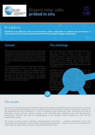
Combined X-ray diffraction and X-ray fluorescence allows researchers to optimize the performance of multi-layered, post-fabricated organic photovoltaic devices doped with gold nanoparticles.

Recommended
More Related Content
What's hot
What's hot (20)
Similar to Organic solar cells probed in situ
Similar to Organic solar cells probed in situ (20)
More from Platform for Advanced Characterisation Grenoble (PAC-G)
More from Platform for Advanced Characterisation Grenoble (PAC-G) (7)
Recently uploaded
Recently uploaded (20)
Organic solar cells probed in situ
- 1. The results The accuracy of the technique made it possible to measure the nanoparticle distribution profile across the device thickness, with in situ measurements providing a space-resolved description of the molecular ordering of the polymer component of the photoactive layer. This information is crucial for developing higher performing solar cells because the rate of photovoltaic energy conversion depends strongly on the nanoscale phase separation during the donor/acceptor heterojunction formation and also on nanomorphology of the interfaces formed between the active and the charge-collecting layer. The results uncovered several underlying chemical-physical phenomena -- including modification of the local nanostructure and organisation, interface effects and inter-diffusion processes – that occur due to the annealing process used to optimise organic solar cell efficiency (Advanced Materials 25 4760). The challenge Unlike silicon PV cells, the efficiency of organic PV cells is poor and decreases markedly over time. For such technologies to become mature enough for routine industrial production, novel solutions must be found to harvest light more efficiently. By introducing metallic nanoparticles to the polymer layer, localized surface plasmon resonances strongly absorb light in the UV–visible band and thus promise high performance and durable solar cells. Combined vertical scanning X-ray diffraction and fluorescence spectroscopy at ESRF beamline ID11 has allowed researchers to obtain detailed characterisation of a post-fabricated multilayered organic electronic device coated with gold nanoparticles. Laboratory-based techniques alone are insufficient to probe the sandwich-type geometry of organic photovoltaic cells, but the high penetration depth and small spot size of synchrotron X-rays allow changes in the nanoparticle distribution and structural properties of the organic layer to be monitored as a function of device depth. Combined X-ray diffraction and X-ray fluorescence allows researchers to optimize the performance of multi-layered, post-fabricated organic photovoltaic devices doped with gold nanoparticles. At a glance: Context Photovoltaic (PV) cells are a key element of a sustainable energy future, with numerous device architectures under development to maximize the conversion of sunlight into electricity. The best performing cells are made from silicon, but organic polymer based PV cells offer a cheap and mass producible alternative with a low environmental impact. A highly promising organic PV architecture comprises a bulk heterojunction polymer made from nanoscale donor-acceptor blends -- typically a conjugated polymer and a soluble fullerene derivative. Such devices, thanks to the ease of chemical processing and the lowcost fabrication of thin films, could herald a technological revolution that allows flexible, transparent solar cells to be painted onto walls or windows. Organic solar cells probed in situ
- 2. The technique ▪ In X-ray diffraction (XRD) beams of X-rays are deflected by crystalline matter to produce a characteristic diffraction pattern that depends on a sample’s atomic structure, while X-ray fluorescence (XRF) probes the elemental composition of samples. ▪ Combining XRD and XRF with nanometre resolution allows detailed in situ studies of multilayered systems such as organic photovoltaic devices doped with gold nanoparticles. ▪ In order to characterize the inner workings of devices, samples must take the form of a cross sectional slice that is measured end-on using X-rays. ▪ The sample is translated vertically through the Xray beam while continuously recording diffraction patterns with a 2D detector. ▪ By scanning the sample cross-section with a 100 nm focused X-ray beam, structural properties of the different layers and interfaces within the device can be studied in situ. Conclusion Powerful in situ spatially resolved studies have revealed the detailed structure of post-fabricated multilayered organic electronic devices, revealing the mechanisms leading to the structural properties of the different organic layers and interfaces. New insight has been gained into the role of plasmonic nanoparticles, representing a milestone towards a better understanding of how the performance of organic photovoltaic cells is correlated to the morphology of their respective components on the nanoscale. Thanks to the high spatial resolution achieved at the ID11 beamline these results represent a major step towards the elucidation of structure-property relations that link different length scales ranging from local nano/hetero structures and interfaces to large-scale devices. The technique is applicable to any thin-film device and coating, and forthcoming advances in modern nanofocusing X-ray optics will allow detailed studies of virtually any type of multilayered organic electronic device on all relevant length scales. In X-ray diffraction (XRD) beams of X-rays are deflected by crystalline matter to produce a Powerful in situ spatially resolved studies have revealed the detailed structure of post-fabricated multilayered organic electronic devices, revealing c Fluorescence line intensities versus vertical scanning step for each metallic element in an organic photovoltaic device sandwiched between an aluminium electrode and indium tin oxide layer, and containing gold nanoparticles to enhance device efficiency. a b Get in touch today for further details:Get in touch today for further details:Get in touch today for further details:Get in touch today for further details: Ennio Capria capria.eu | +33 4 76 88 29 05 www.irtnanoelec.fr 71 Avenue des Martyrs, 38000 Grenoble Cedex 09 - FRANCE deflected by crystalline matter to produce a characteristic diffraction pattern that depends on a sample’s atomic structure, while X-ray fluorescence (XRF) probes the elemental composition of samples. Combining XRD and XRF with nanometre resolution allows detailed in situ studies of multi- layered systems such as organic photovoltaic devices doped with gold nanoparticles. In order to characterize the inner workings of devices, samples must take the form of a cross sectional slice that is measured end-on using X-rays. The sample is translated vertically through the X- ray beam while continuously recording diffraction patterns with a 2D detector. By scanning the sample cross-section with a 100 nm focused X-ray beam, structural properties of the different layers and interfaces within the device can be studied in situ. multilayered organic electronic devices, revealing the mechanisms leading to the structural properties of the different organic layers and interfaces. New insight has been gained into the role of plasmonic nanoparticles, representing a milestone towards a better understanding of how the performance of organic photovoltaic cells is correlated to the morphology of their respective components on the nanoscale. Thanks to the high spatial resolution achieved at the ID11 beamline these results represent a major step towards the elucidation of structure-property relations that link different length scales ranging from local nano/hetero structures and interfaces to large-scale devices. The technique is applicable to any thin-film device and coating, and forthcoming advances in modern nanofocusing X-ray optics will allow detailed studies of virtually any type of multilayered organic electronic device on all relevant length scales.