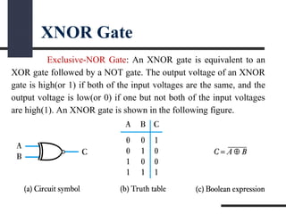
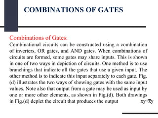
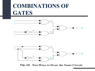
Download to read offline
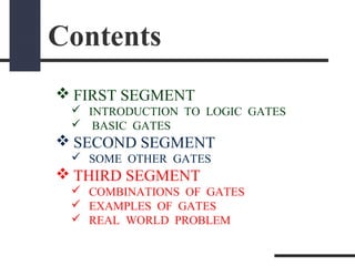
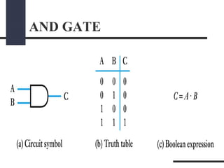
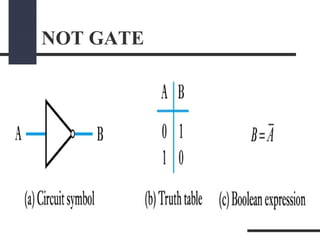

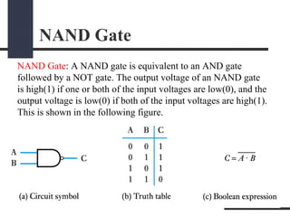
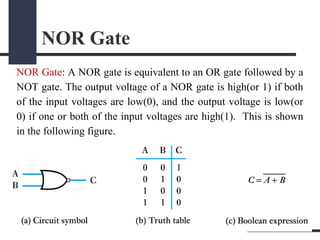
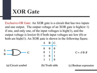

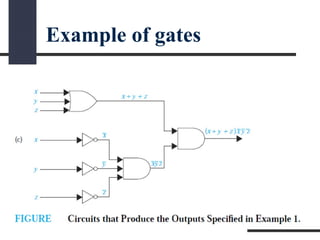
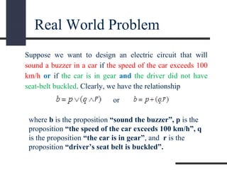
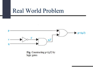


This document presents a presentation on logic gates such as OR, AND, and NOT gates. It begins with an introduction to logic gates and Boolean algebra. It then describes the basic OR, AND, and NOT gates. The presentation continues by explaining some other gates like NAND, NOR, XOR and XNOR gates. It provides an example of combining gates. Finally, it proposes a real-world problem of designing a car circuit to sound a buzzer based on speed or seatbelt use and shows the logic gate implementation of the solution.