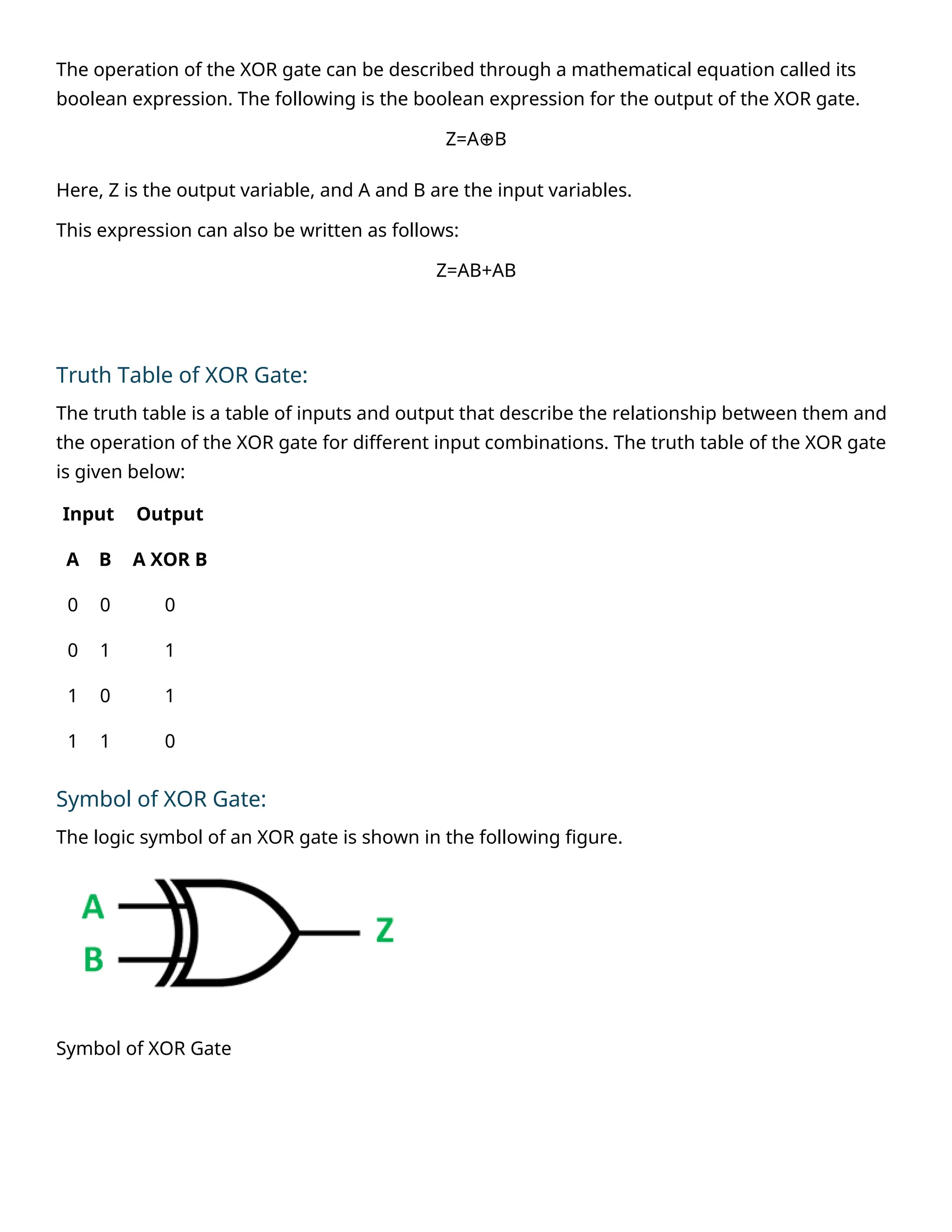
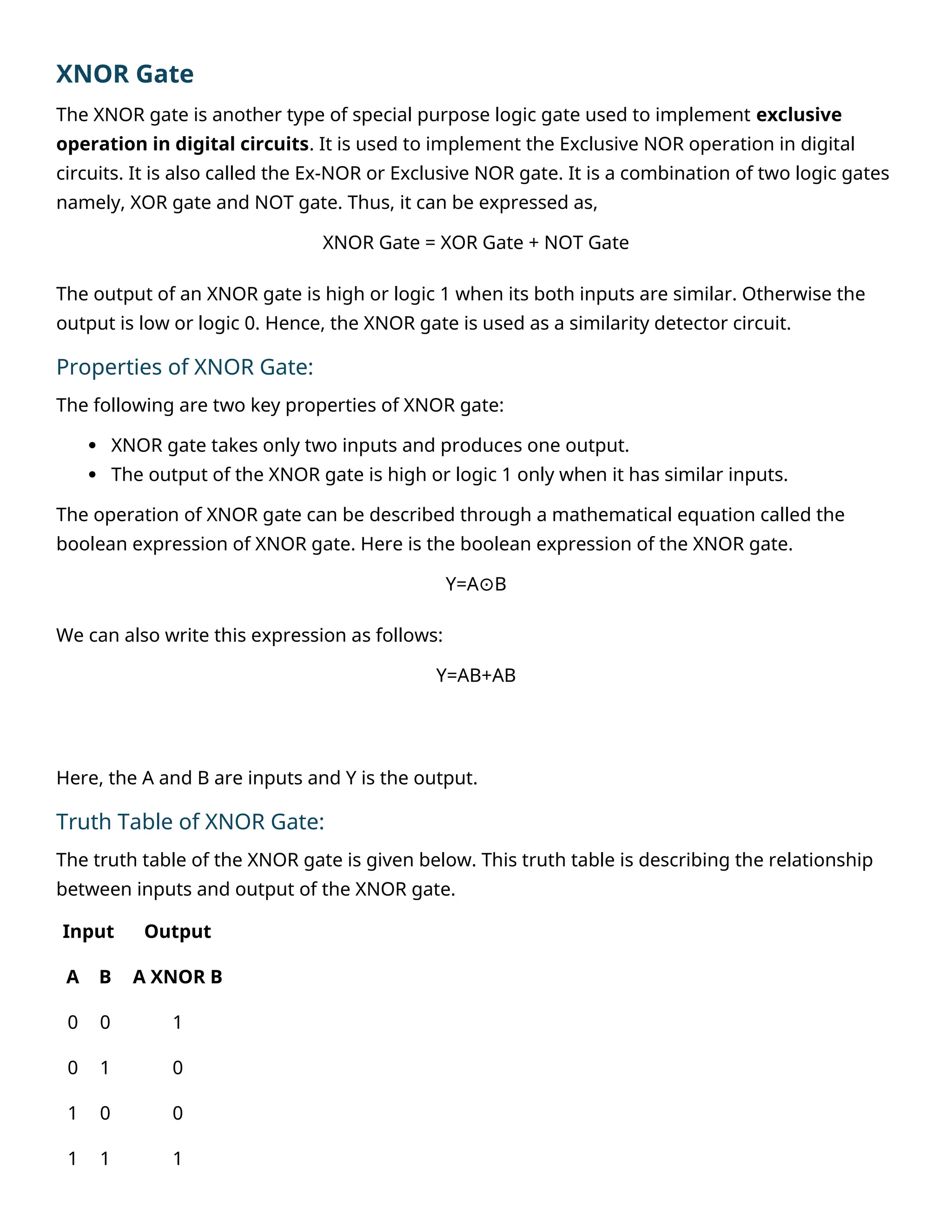
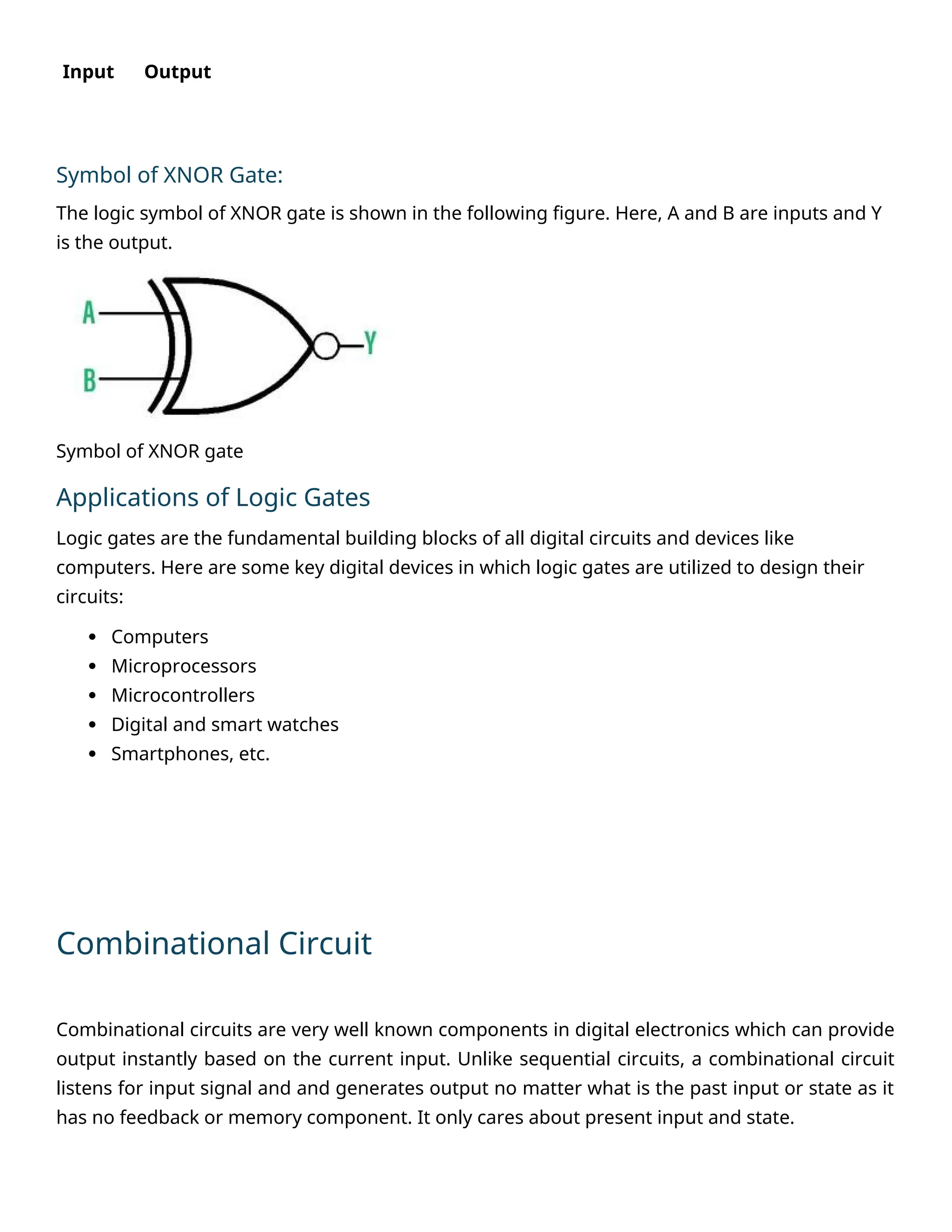
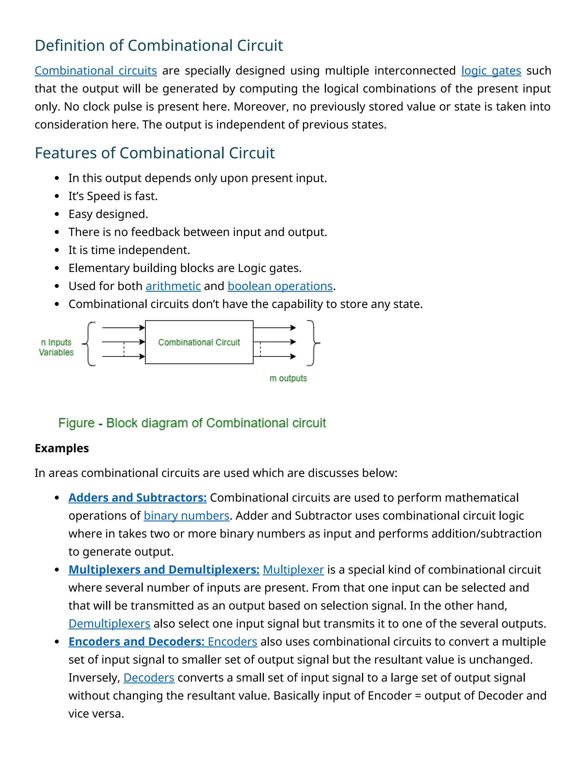
BCA5B07 - Computer Organization and Architecture
Unit I [12 T] Digital Logic - Positive and negative logic, logic gates ,NOT gate, OR gate, AND gate,
XOR and X-NOR gates, Universal gates- NAND gate, NOR gate,. Combinational circuits- Half
adder, half subtractor, full adder, full subtractor, ripple carry adders, look-ahead carry adders,
decoders, BCD to 7-segment decoder, encoders, multiplexers and demultiplexers.
=============================================================================--
-------------------------------------------------------------------------------------------------------------------------------------
Digital Logic
Digital logic is the foundation of digital circuits, which are the building blocks of all electronic
devices such as computers, smartphones, and digital appliances. It involves the use of binary
numbers (0s and 1s) to represent and process information.
Positive and negative logic
All digital systems use the binary number system. Hence, all the digital electronic systems have
two states namely, HIGH and LOW, where HIGH is represented by Binary 1 and LOW is
represented by Binary 0.
Based on the system response, The logic in digital electronics is classified into two types −
 Positive Logic
 Negative Logic
The case of positive logic,
The voltage at 0 volts level represents the logic 0 (Logic LOW), and
the voltage at +VCC volts level represents the logic 1 (Logic HIGH).
In the generalized form, the positive logic is expressed as,
HigherVoltage=LogicHIGH (1)
LowerVoltage=LogicLOW (0)
The case of negative logic,
The voltage at -VCC volts level represents the logic 0 (Logic LOW), and
the voltage at 0 volts level represents the logic 1 (Logic HIGH).
In the generalized form, the negative logic is expressed as,
HigherVoltage=LogicLOW(0)
LowerVoltage=LogicHIGH(1)
Logic Gates – Definition, Types, Uses
Logic gates are the fundamental components of all digital circuits and systems.
It is a physical device which perform logical operation on one or more logical inputs and produce a
single logical output
A logic gate is basically an electronic circuit designed by using components like diodes,
transistors, resistors, capacitors, etc., and capable of performing logical operations.
Logic gates use Boolean algebra to execute logical processes. Logic gates are found in nearly every
digital gadget we use on a regular basis. Logic gates are used in the architecture of our
telephones, laptops, tablets, and memory devices.
In digital electronics, there are seven main types of logic gates used to perform various logical
operations.
Types of Logic Gates
1. Basic Logic Gates
There are three basic logic gates:
1. AND Gate
2. OR Gate
3. NOT Gate
2. Universal Logic Gates
In digital electronics, the following two logic gates are considered as universal logic gates:
4. NOR Gate
5. NAND Gate
3. Derived Logic Gates
The following two are the derived logic gates used in digital systems:
6. XOR Gate
7. XNOR Gate
AND Gate
The AND gate is one of the basic logic gate that performs the logical multiplication of inputs
applied to it. It generates a high or logic 1 output, only when all the inputs applied to it are high
or logic 1. Otherwise, the output of the AND gate is low or logic 0.
Properties of AND Gate:
The following are two main properties of the AND gate:
 AND gate can accept two or more than two input values at a time.
 When all of the inputs are logic 1, the output of this gate is logic 1.
The operation of an AND gate is described by a mathematical expression, which is called the
Boolean expression of the AND gate.
For two-input AND gate, the Boolean expression is given by,
𝑍=𝐴.𝐵
Where, A and B are inputs to the AND gate, while Z denotes the output of the AND gate.
We can extend this expression to any number of input variables, such as,
𝑍=𝐴.𝐵.𝐶.𝐷…
Truth Table of AND Gate:
The truth table of a two input AND gate is given below:
Input Output
A B
A AND B
(A.B)
0 0 0
0 1 0
1 0 0
1 1 1
Symbol of AND Gate:
The logic symbol of a two input AND gate is shown in the following figure.
OR Gate
In digital electronics, there is a type of basic logic gate which produces a low or logic
0 output only when its all inputs are low or logic 0. For all other input combinations,
the output of the OR gate is high or logic 1. This logic gate is termed as OR gate. An
OR gate can be designed to have two or more inputs but only one output. The
primary function of the OR gate is to perform the logical sum operation.
Properties of OR Gate:
An OR gate have the following two properties:
 It can have two or more input lines at a time.
 When all of the inputs to the OR gate are low or logic 0, the output of it is low or
logic 0.
The operation of an OR gate can be mathematically described through a
mathematical expression called Boolean expression of the OR gate.
The boolean expression for a two input OR gate is given by,
Z = A + B
The boolean expression for a three-input OR gate is,
Z = A + B + C
Here, A, B, and C are inputs and Z is the output variables. We can extend this boolean
expression to any number of input variables.
Truth Table of OR Gate:
The truth table of an OR gate describes the relationship between inputs and output.
The following is the truth table for the two-input OR gate:
Input Output
A B A OR B
0 0 0
0 1 1
1 0 1
1 1 1
Symbol of OR Gate:
The logic symbol of a two-input OR gate is shown in the following figure.
NOT Gate
In digital electronics, the NOT gate is another basic logic gate used to perform compliment of
an input signal applied to it. It takes only one input and one output. The output of the NOT
gate is complement of the input applied to it. Therefore, if we apply a low or logic 0 output to
the NOT gate is gives a high or logic 1 output and vice-versa. The NOT gate is also known as
inverter, as it performs the inversion operation.
Properties of NOT Gate:
 The output of a NOT gate is complement or inverse of the input applied to it.
 NOT gate takes only one output.
The logical operation of the NOT gate is described by its boolean expression, which is given
below.
Z=A
The bar over the input variable A represents the inversion operation.
Truth Table of OR Gate:
The truth table describes the relationship between input and output. The following is the truth
table for the NOT gate:
Input Output
A NOT A
0 1
1 0
Symbol of NOT Gate
The logic circuit symbol of a NOT gate is shown in the following figure. Here, A is the input line
and Z is the output line.
Symbol of NOT the Gate
NOR Gate
The NOR gate is a type of universal logic gate that can take two or more inputs but one output.
It is basically a combination of two basic logic gates i.e., OR gate and NOT gate. Thus, it can be
expressed as,
NOR Gate = OR Gate + NOT Gate
In other words, a NOR gate is an OR gate followed by a NOT gate.
Properties of NOR Gate:
The following are two important properties of NOR gate:
 A NOR gate can have two or more inputs and gives an output.
 A NOR gate gives a high or logic 1 output only when its all inputs are low or logic 0.
Similar to basic logic gates, we can describe the operation of a NOR gate using a mathematical
equation called boolean expression of the NOR gate.
The boolean expression of a two input NOR gate is given below:
C=A+B
We can extend this expression to any number of input variables.
In the above boolean expressions, the variables A and B are called input variables while the
variable C is called the output variable.
Truth Table of NOR Gate:
The following is the truth table of a two-input NOR gate showing the relationship between its
inputs and output:
Input Output
A B A NOR B
0 0 1
0 1 0
1 0 0
1 1 0
Symbol of the NOR Gate
NAND Gate
In digital electronics, the NAND gate is another type of universal logic gate used to perform
logical operations. The NAND gate performs the inverted operation of the AND gate. Similar to
NOR gate, the NAND gate can also have two or more input lines but only one output line.
The NAND gate is also represented as a combination of two basic logic gates namely, AND gate
and NOT gate. Hence, it can be expressed as
NAND Gate = AND Gate + NOT Gate
Properties of NAND Gate:
The following are the two key properties of NAND gate:
 NAND gate can take two or more inputs at a time and produces one output based on the
combination of inputs applied.
 NAND gate produces a low or logic 0 output only when its all inputs are high or logic 1.
We can describe the expression of NAND gate through a mathematical equation called its
boolean expression. Here is the boolean expression of a two input NAND gate.
C=AB
In this expression, A and B are the input variables and C is the output variable. We can extend
this relation to any number of input variables like three, four, or more.
Truth Table of NAND Gate:
The truth table is a table of inputs and output that describes the operation of the NAND gate
and shows the logical relationship between them:
Input Output
A B A NAND B
0 0 1
0 1 1
1 0 1
1 1 0
Symbol of NAND Gate:
The logic symbol of a NAND gate is represented as a AND gate with a bubble on its output end
as depicted in the following figure. It is the symbol of a two-input NAND gate.
Symbol of NAND Gate
XOR Gate
In digital electronics, there is a specially designed logic gate named, XOR gate, which is used in
digital circuits to perform modulo sum. It is also referred to as Exclusive OR gate or Ex-OR
gate. The XOR gate can take only two inputs at a time and give an output. The output of the
XOR gate is high or logic 1 only when its two inputs are dissimilar.
Properties of XOR Gate:
The following two are the main properties of the XOR gate:
 It can accept only two inputs at a time. There is nothing like a three or more input XOR
gate.
 The output of the XOR gate is logic 1 or high, when its inputs are dissimilar.
The operation of the XOR gate can be described through a mathematical equation called its
boolean expression. The following is the boolean expression for the output of the XOR gate.
Z=A B
⊕
Here, Z is the output variable, and A and B are the input variables.
This expression can also be written as follows:
Z=AB+AB
Truth Table of XOR Gate:
The truth table is a table of inputs and output that describe the relationship between them and
the operation of the XOR gate for different input combinations. The truth table of the XOR gate
is given below:
Input Output
A B A XOR B
0 0 0
0 1 1
1 0 1
1 1 0
Symbol of XOR Gate:
The logic symbol of an XOR gate is shown in the following figure.
Symbol of XOR Gate
XNOR Gate
The XNOR gate is another type of special purpose logic gate used to implement exclusive
operation in digital circuits. It is used to implement the Exclusive NOR operation in digital
circuits. It is also called the Ex-NOR or Exclusive NOR gate. It is a combination of two logic gates
namely, XOR gate and NOT gate. Thus, it can be expressed as,
XNOR Gate = XOR Gate + NOT Gate
The output of an XNOR gate is high or logic 1 when its both inputs are similar. Otherwise the
output is low or logic 0. Hence, the XNOR gate is used as a similarity detector circuit.
Properties of XNOR Gate:
The following are two key properties of XNOR gate:
 XNOR gate takes only two inputs and produces one output.
 The output of the XNOR gate is high or logic 1 only when it has similar inputs.
The operation of XNOR gate can be described through a mathematical equation called the
boolean expression of XNOR gate. Here is the boolean expression of the XNOR gate.
Y=A B
⊙
We can also write this expression as follows:
Y=AB+AB
Here, the A and B are inputs and Y is the output.
Truth Table of XNOR Gate:
The truth table of the XNOR gate is given below. This truth table is describing the relationship
between inputs and output of the XNOR gate.
Input Output
A B A XNOR B
0 0 1
0 1 0
1 0 0
1 1 1
Input Output
Symbol of XNOR Gate:
The logic symbol of XNOR gate is shown in the following figure. Here, A and B are inputs and Y
is the output.
Symbol of XNOR gate
Applications of Logic Gates
Logic gates are the fundamental building blocks of all digital circuits and devices like
computers. Here are some key digital devices in which logic gates are utilized to design their
circuits:
 Computers
 Microprocessors
 Microcontrollers
 Digital and smart watches
 Smartphones, etc.
Combinational Circuit
Combinational circuits are very well known components in digital electronics which can provide
output instantly based on the current input. Unlike sequential circuits, a combinational circuit
listens for input signal and and generates output no matter what is the past input or state as it
has no feedback or memory component. It only cares about present input and state.
Definition of Combinational Circuit
Combinational circuits are specially designed using multiple interconnected logic gates such
that the output will be generated by computing the logical combinations of the present input
only. No clock pulse is present here. Moreover, no previously stored value or state is taken into
consideration here. The output is independent of previous states.
Features of Combinational Circuit
 In this output depends only upon present input.
 It’s Speed is fast.
 Easy designed.
 There is no feedback between input and output.
 It is time independent.
 Elementary building blocks are Logic gates.
 Used for both arithmetic and boolean operations.
 Combinational circuits don’t have the capability to store any state.
Examples
In areas combinational circuits are used which are discusses below:
 Adders and Subtractors: Combinational circuits are used to perform mathematical
operations of binary numbers. Adder and Subtractor uses combinational circuit logic
where in takes two or more binary numbers as input and performs addition/subtraction
to generate output.
 Multiplexers and Demultiplexers: Multiplexer is a special kind of combinational circuit
where several number of inputs are present. From that one input can be selected and
that will be transmitted as an output based on selection signal. In the other hand,
Demultiplexers also select one input signal but transmits it to one of the several outputs.
 Encoders and Decoders: Encoders also uses combinational circuits to convert a multiple
set of input signal to smaller set of output signal but the resultant value is unchanged.
Inversely, Decoders converts a small set of input signal to a large set of output signal
without changing the resultant value. Basically input of Encoder = output of Decoder and
vice versa.
Applications of Combinational Circuit
In modern technologies, combinational circuits are widely used for its simple functionality and
ability to give instant output. Some of the applications are discussed below:
 Arithmetic and Logic Units (ALUs): As combinational circuits are capable of performing
various mathematical tasks like arithmetic and logical operations so, these circuits are
used in calculators and processors as a fundamental component of ALU.
 Data Encryption and Decryption: In information protection fields, combinational circuit
are used for encryption and decryption of data for secure communication.
Encryption/decryption algorithms are also a complex mathematical formula which can be
performed by combinational circuits.
 Data Multiplexing and Demultiplexing: It is just a practical implementation of
multiplexer and demultiplexer. By using it we can optimize network bandwidth by
effectively reducing network traffic as combinational circuit allows to transmit multiple
data signals over a single communication channel.
 Traffic Light Control: In traffic lights control mechanism, combinational circuits are used
to instantly determine the timing and sequence of traffic light changes based on the
inputs of timers and sensors.
Advantages of Combinational Circuit
Some basic advantages of combinational circuits has made them very popular among modern
technologies which are discussed below:
 Simplicity: Combinational circuits are very easy to implement and absence of memory or
feedback element has made it more straightforward which is reducing complexity in
digital systems and providing faster prototype building mechanism.
 Real-time Operation: Combinational circuits don’t face any delay which is very much
essential for quick-response applications like data transmission and signal processing.
 Deterministic Behavior: Combinational circuits generate output based on present input
only which ensures predictable and repeatable results which is essential for applications
in which consistency and reliability is required.
Disadvantages of Combinational Circuit
 Limited Functionality: As it provides output only based on present input and there is no
way to store previous data so we can’t use this circuit to any memory-based applications
or where previous data is recalled for doing operations.
 Lack of Flexibility: Once the design of logic gates is done then for changing a small
design required the entire redesigning of the circuits which is monotonous and time-
consuming.
 Increased Complexity for Large Designs: For large designs the number of logic gates
will increase gradually which means the management of input and output ports will
become very complex. This may lead to higher production costs and increased design
errors.

combinational-circuit____gates_456788 (2).docx

  • 1.
    BCA5B07 - ComputerOrganization and Architecture Unit I [12 T] Digital Logic - Positive and negative logic, logic gates ,NOT gate, OR gate, AND gate, XOR and X-NOR gates, Universal gates- NAND gate, NOR gate,. Combinational circuits- Half adder, half subtractor, full adder, full subtractor, ripple carry adders, look-ahead carry adders, decoders, BCD to 7-segment decoder, encoders, multiplexers and demultiplexers. =============================================================================-- ------------------------------------------------------------------------------------------------------------------------------------- Digital Logic Digital logic is the foundation of digital circuits, which are the building blocks of all electronic devices such as computers, smartphones, and digital appliances. It involves the use of binary numbers (0s and 1s) to represent and process information. Positive and negative logic All digital systems use the binary number system. Hence, all the digital electronic systems have two states namely, HIGH and LOW, where HIGH is represented by Binary 1 and LOW is represented by Binary 0. Based on the system response, The logic in digital electronics is classified into two types −  Positive Logic  Negative Logic The case of positive logic, The voltage at 0 volts level represents the logic 0 (Logic LOW), and the voltage at +VCC volts level represents the logic 1 (Logic HIGH). In the generalized form, the positive logic is expressed as, HigherVoltage=LogicHIGH (1) LowerVoltage=LogicLOW (0)
  • 2.
    The case ofnegative logic, The voltage at -VCC volts level represents the logic 0 (Logic LOW), and the voltage at 0 volts level represents the logic 1 (Logic HIGH). In the generalized form, the negative logic is expressed as, HigherVoltage=LogicLOW(0) LowerVoltage=LogicHIGH(1) Logic Gates – Definition, Types, Uses Logic gates are the fundamental components of all digital circuits and systems. It is a physical device which perform logical operation on one or more logical inputs and produce a single logical output A logic gate is basically an electronic circuit designed by using components like diodes, transistors, resistors, capacitors, etc., and capable of performing logical operations. Logic gates use Boolean algebra to execute logical processes. Logic gates are found in nearly every digital gadget we use on a regular basis. Logic gates are used in the architecture of our telephones, laptops, tablets, and memory devices. In digital electronics, there are seven main types of logic gates used to perform various logical operations. Types of Logic Gates 1. Basic Logic Gates There are three basic logic gates: 1. AND Gate
  • 3.
    2. OR Gate 3.NOT Gate 2. Universal Logic Gates In digital electronics, the following two logic gates are considered as universal logic gates: 4. NOR Gate 5. NAND Gate 3. Derived Logic Gates The following two are the derived logic gates used in digital systems: 6. XOR Gate 7. XNOR Gate AND Gate The AND gate is one of the basic logic gate that performs the logical multiplication of inputs applied to it. It generates a high or logic 1 output, only when all the inputs applied to it are high or logic 1. Otherwise, the output of the AND gate is low or logic 0. Properties of AND Gate: The following are two main properties of the AND gate:  AND gate can accept two or more than two input values at a time.  When all of the inputs are logic 1, the output of this gate is logic 1. The operation of an AND gate is described by a mathematical expression, which is called the Boolean expression of the AND gate. For two-input AND gate, the Boolean expression is given by, 𝑍=𝐴.𝐵 Where, A and B are inputs to the AND gate, while Z denotes the output of the AND gate. We can extend this expression to any number of input variables, such as, 𝑍=𝐴.𝐵.𝐶.𝐷…
  • 4.
    Truth Table ofAND Gate: The truth table of a two input AND gate is given below: Input Output A B A AND B (A.B) 0 0 0 0 1 0 1 0 0 1 1 1 Symbol of AND Gate: The logic symbol of a two input AND gate is shown in the following figure. OR Gate In digital electronics, there is a type of basic logic gate which produces a low or logic 0 output only when its all inputs are low or logic 0. For all other input combinations, the output of the OR gate is high or logic 1. This logic gate is termed as OR gate. An
  • 5.
    OR gate canbe designed to have two or more inputs but only one output. The primary function of the OR gate is to perform the logical sum operation. Properties of OR Gate: An OR gate have the following two properties:  It can have two or more input lines at a time.  When all of the inputs to the OR gate are low or logic 0, the output of it is low or logic 0. The operation of an OR gate can be mathematically described through a mathematical expression called Boolean expression of the OR gate. The boolean expression for a two input OR gate is given by, Z = A + B The boolean expression for a three-input OR gate is, Z = A + B + C Here, A, B, and C are inputs and Z is the output variables. We can extend this boolean expression to any number of input variables. Truth Table of OR Gate: The truth table of an OR gate describes the relationship between inputs and output. The following is the truth table for the two-input OR gate: Input Output A B A OR B 0 0 0 0 1 1
  • 6.
    1 0 1 11 1 Symbol of OR Gate: The logic symbol of a two-input OR gate is shown in the following figure. NOT Gate In digital electronics, the NOT gate is another basic logic gate used to perform compliment of an input signal applied to it. It takes only one input and one output. The output of the NOT gate is complement of the input applied to it. Therefore, if we apply a low or logic 0 output to the NOT gate is gives a high or logic 1 output and vice-versa. The NOT gate is also known as inverter, as it performs the inversion operation. Properties of NOT Gate:  The output of a NOT gate is complement or inverse of the input applied to it.  NOT gate takes only one output. The logical operation of the NOT gate is described by its boolean expression, which is given below. Z=A The bar over the input variable A represents the inversion operation. Truth Table of OR Gate: The truth table describes the relationship between input and output. The following is the truth table for the NOT gate:
  • 7.
    Input Output A NOTA 0 1 1 0 Symbol of NOT Gate The logic circuit symbol of a NOT gate is shown in the following figure. Here, A is the input line and Z is the output line. Symbol of NOT the Gate NOR Gate The NOR gate is a type of universal logic gate that can take two or more inputs but one output. It is basically a combination of two basic logic gates i.e., OR gate and NOT gate. Thus, it can be expressed as, NOR Gate = OR Gate + NOT Gate In other words, a NOR gate is an OR gate followed by a NOT gate. Properties of NOR Gate: The following are two important properties of NOR gate:  A NOR gate can have two or more inputs and gives an output.  A NOR gate gives a high or logic 1 output only when its all inputs are low or logic 0. Similar to basic logic gates, we can describe the operation of a NOR gate using a mathematical equation called boolean expression of the NOR gate. The boolean expression of a two input NOR gate is given below:
  • 8.
    C=A+B We can extendthis expression to any number of input variables. In the above boolean expressions, the variables A and B are called input variables while the variable C is called the output variable. Truth Table of NOR Gate: The following is the truth table of a two-input NOR gate showing the relationship between its inputs and output: Input Output A B A NOR B 0 0 1 0 1 0 1 0 0 1 1 0 Symbol of the NOR Gate NAND Gate In digital electronics, the NAND gate is another type of universal logic gate used to perform logical operations. The NAND gate performs the inverted operation of the AND gate. Similar to NOR gate, the NAND gate can also have two or more input lines but only one output line. The NAND gate is also represented as a combination of two basic logic gates namely, AND gate and NOT gate. Hence, it can be expressed as NAND Gate = AND Gate + NOT Gate Properties of NAND Gate: The following are the two key properties of NAND gate:
  • 9.
     NAND gatecan take two or more inputs at a time and produces one output based on the combination of inputs applied.  NAND gate produces a low or logic 0 output only when its all inputs are high or logic 1. We can describe the expression of NAND gate through a mathematical equation called its boolean expression. Here is the boolean expression of a two input NAND gate. C=AB In this expression, A and B are the input variables and C is the output variable. We can extend this relation to any number of input variables like three, four, or more.
  • 10.
    Truth Table ofNAND Gate: The truth table is a table of inputs and output that describes the operation of the NAND gate and shows the logical relationship between them: Input Output A B A NAND B 0 0 1 0 1 1 1 0 1 1 1 0 Symbol of NAND Gate: The logic symbol of a NAND gate is represented as a AND gate with a bubble on its output end as depicted in the following figure. It is the symbol of a two-input NAND gate. Symbol of NAND Gate XOR Gate In digital electronics, there is a specially designed logic gate named, XOR gate, which is used in digital circuits to perform modulo sum. It is also referred to as Exclusive OR gate or Ex-OR gate. The XOR gate can take only two inputs at a time and give an output. The output of the XOR gate is high or logic 1 only when its two inputs are dissimilar. Properties of XOR Gate: The following two are the main properties of the XOR gate:  It can accept only two inputs at a time. There is nothing like a three or more input XOR gate.  The output of the XOR gate is logic 1 or high, when its inputs are dissimilar.
  • 11.
    The operation ofthe XOR gate can be described through a mathematical equation called its boolean expression. The following is the boolean expression for the output of the XOR gate. Z=A B ⊕ Here, Z is the output variable, and A and B are the input variables. This expression can also be written as follows: Z=AB+AB Truth Table of XOR Gate: The truth table is a table of inputs and output that describe the relationship between them and the operation of the XOR gate for different input combinations. The truth table of the XOR gate is given below: Input Output A B A XOR B 0 0 0 0 1 1 1 0 1 1 1 0 Symbol of XOR Gate: The logic symbol of an XOR gate is shown in the following figure. Symbol of XOR Gate
  • 12.
    XNOR Gate The XNORgate is another type of special purpose logic gate used to implement exclusive operation in digital circuits. It is used to implement the Exclusive NOR operation in digital circuits. It is also called the Ex-NOR or Exclusive NOR gate. It is a combination of two logic gates namely, XOR gate and NOT gate. Thus, it can be expressed as, XNOR Gate = XOR Gate + NOT Gate The output of an XNOR gate is high or logic 1 when its both inputs are similar. Otherwise the output is low or logic 0. Hence, the XNOR gate is used as a similarity detector circuit. Properties of XNOR Gate: The following are two key properties of XNOR gate:  XNOR gate takes only two inputs and produces one output.  The output of the XNOR gate is high or logic 1 only when it has similar inputs. The operation of XNOR gate can be described through a mathematical equation called the boolean expression of XNOR gate. Here is the boolean expression of the XNOR gate. Y=A B ⊙ We can also write this expression as follows: Y=AB+AB Here, the A and B are inputs and Y is the output. Truth Table of XNOR Gate: The truth table of the XNOR gate is given below. This truth table is describing the relationship between inputs and output of the XNOR gate. Input Output A B A XNOR B 0 0 1 0 1 0 1 0 0 1 1 1
  • 13.
    Input Output Symbol ofXNOR Gate: The logic symbol of XNOR gate is shown in the following figure. Here, A and B are inputs and Y is the output. Symbol of XNOR gate Applications of Logic Gates Logic gates are the fundamental building blocks of all digital circuits and devices like computers. Here are some key digital devices in which logic gates are utilized to design their circuits:  Computers  Microprocessors  Microcontrollers  Digital and smart watches  Smartphones, etc. Combinational Circuit Combinational circuits are very well known components in digital electronics which can provide output instantly based on the current input. Unlike sequential circuits, a combinational circuit listens for input signal and and generates output no matter what is the past input or state as it has no feedback or memory component. It only cares about present input and state.
  • 14.
    Definition of CombinationalCircuit Combinational circuits are specially designed using multiple interconnected logic gates such that the output will be generated by computing the logical combinations of the present input only. No clock pulse is present here. Moreover, no previously stored value or state is taken into consideration here. The output is independent of previous states. Features of Combinational Circuit  In this output depends only upon present input.  It’s Speed is fast.  Easy designed.  There is no feedback between input and output.  It is time independent.  Elementary building blocks are Logic gates.  Used for both arithmetic and boolean operations.  Combinational circuits don’t have the capability to store any state. Examples In areas combinational circuits are used which are discusses below:  Adders and Subtractors: Combinational circuits are used to perform mathematical operations of binary numbers. Adder and Subtractor uses combinational circuit logic where in takes two or more binary numbers as input and performs addition/subtraction to generate output.  Multiplexers and Demultiplexers: Multiplexer is a special kind of combinational circuit where several number of inputs are present. From that one input can be selected and that will be transmitted as an output based on selection signal. In the other hand, Demultiplexers also select one input signal but transmits it to one of the several outputs.  Encoders and Decoders: Encoders also uses combinational circuits to convert a multiple set of input signal to smaller set of output signal but the resultant value is unchanged. Inversely, Decoders converts a small set of input signal to a large set of output signal without changing the resultant value. Basically input of Encoder = output of Decoder and vice versa.
  • 15.
    Applications of CombinationalCircuit In modern technologies, combinational circuits are widely used for its simple functionality and ability to give instant output. Some of the applications are discussed below:  Arithmetic and Logic Units (ALUs): As combinational circuits are capable of performing various mathematical tasks like arithmetic and logical operations so, these circuits are used in calculators and processors as a fundamental component of ALU.  Data Encryption and Decryption: In information protection fields, combinational circuit are used for encryption and decryption of data for secure communication. Encryption/decryption algorithms are also a complex mathematical formula which can be performed by combinational circuits.  Data Multiplexing and Demultiplexing: It is just a practical implementation of multiplexer and demultiplexer. By using it we can optimize network bandwidth by effectively reducing network traffic as combinational circuit allows to transmit multiple data signals over a single communication channel.  Traffic Light Control: In traffic lights control mechanism, combinational circuits are used to instantly determine the timing and sequence of traffic light changes based on the inputs of timers and sensors. Advantages of Combinational Circuit Some basic advantages of combinational circuits has made them very popular among modern technologies which are discussed below:  Simplicity: Combinational circuits are very easy to implement and absence of memory or feedback element has made it more straightforward which is reducing complexity in digital systems and providing faster prototype building mechanism.  Real-time Operation: Combinational circuits don’t face any delay which is very much essential for quick-response applications like data transmission and signal processing.  Deterministic Behavior: Combinational circuits generate output based on present input only which ensures predictable and repeatable results which is essential for applications in which consistency and reliability is required. Disadvantages of Combinational Circuit  Limited Functionality: As it provides output only based on present input and there is no way to store previous data so we can’t use this circuit to any memory-based applications or where previous data is recalled for doing operations.  Lack of Flexibility: Once the design of logic gates is done then for changing a small design required the entire redesigning of the circuits which is monotonous and time- consuming.
  • 16.
     Increased Complexityfor Large Designs: For large designs the number of logic gates will increase gradually which means the management of input and output ports will become very complex. This may lead to higher production costs and increased design errors.