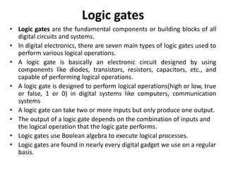
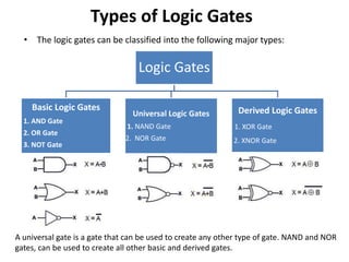
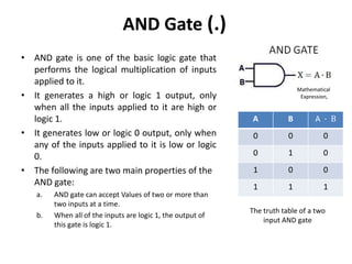
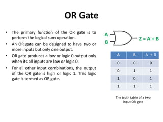
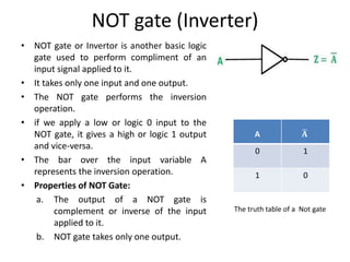
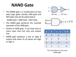
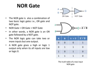
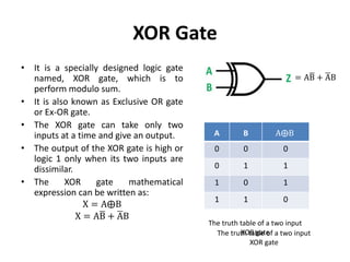
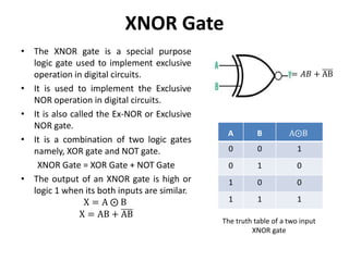
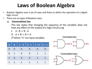
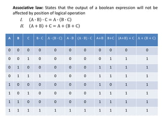
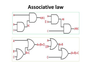
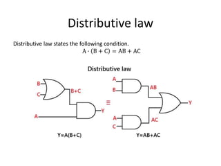
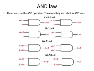
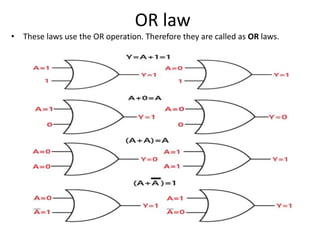
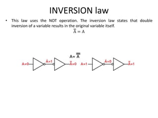
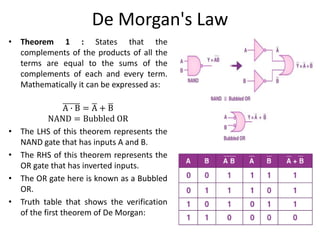
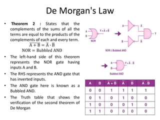
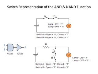
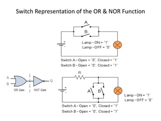
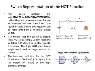
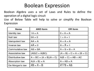
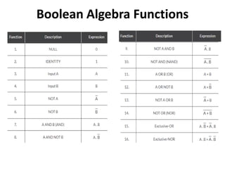
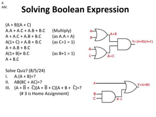
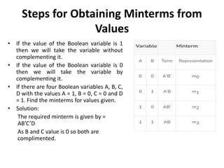
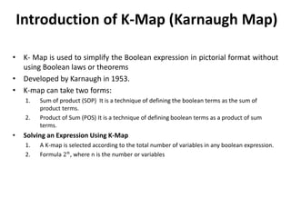
Digital Logic Design
Logic Gates
Boolean Algebra
Karnaugh Map (K-Map)
Logic gates
• Logic gates are the fundamental components or building blocks of all
digital circuits and systems.
• In digital electronics, there are seven main types of logic gates used to
perform various logical operations.
• A logic gate is basically an electronic circuit designed by using
components like diodes, transistors, resistors, capacitors, etc., and
capable of performing logical operations.
• A logic gate is designed to perform logical operations(high or low, true
or false, 1 or 0) in digital systems like computers, communication
systems
• A logic gate can take two or more inputs but only produce one output.
• The output of a logic gate depends on the combination of inputs and
the logical operation that the logic gate performs.
• Logic gates use Boolean algebra to execute logical processes.
• Logic gates are found in nearly every digital gadget we use on a regular
basis.
Types of Logic Gates
• The logic gates can be classified into the following major types:
Logic Gates
Basic Logic Gates
1. AND Gate
2. OR Gate
3. NOT Gate
Universal Logic Gates
1. NAND Gate
2. NOR Gate
Derived Logic Gates
1. XOR Gate
2. XNOR Gate
A universal gate is a gate that can be used to create any other type of gate. NAND and NOR
gates, can be used to create all other basic and derived gates.
AND Gate (.)
• AND gate is one of the basic logic gate that
performs the logical multiplication of inputs
applied to it.
• It generates a high or logic 1 output, only
when all the inputs applied to it are high or
logic 1.
• It generates low or logic 0 output, only when
any of the inputs applied to it is low or logic
0.
• The following are two main properties of the
AND gate:
a. AND gate can accept Values of two or more than
two inputs at a time.
b. When all of the inputs are logic 1, the output of
this gate is logic 1.
A B A ∙ B
0 0 0
0 1 0
1 0 0
1 1 1
Mathematical
Expression,
The truth table of a two
input AND gate
OR Gate
• The primary function of the OR gate is to
perform the logical sum operation.
• An OR gate can be designed to have two or
more inputs but only one output.
• OR gate produces a low or logic 0 output only
when its all inputs are low or logic 0.
• For all other input combinations, the output
of the OR gate is high or logic 1. This logic
gate is termed as OR gate.
A B A + B
0 0 0
0 1 1
1 0 1
1 1 1
The truth table of a two
input OR gate
NOT gate (Inverter)
• NOT gate or Invertor is another basic logic
gate used to perform compliment of an
input signal applied to it.
• It takes only one input and one output.
• The NOT gate performs the inversion
operation.
• if we apply a low or logic 0 input to the
NOT gate, it gives a high or logic 1 output
and vice-versa.
• The bar over the input variable A
represents the inversion operation.
• Properties of NOT Gate:
a. The output of a NOT gate is
complement or inverse of the input
applied to it.
b. NOT gate takes only one output.
A 𝐀
0 1
1 0
The truth table of a Not gate
NAND Gate
• The NAND gate is a combination of two
basic logic gates namely, AND gate and
NOT gate and can be expressed as
NAND Gate = AND Gate + NOT Gate
• The NAND gate performs the inverted
operation of the AND gate.
• Similar to NOR gate, it can have two or
more input lines but only one output
line.
• NAND gate produces a low or logic 0
output only when its all inputs are high
or logic 1.
A B A ∙ B 𝐀 ∙ 𝐁
0 0 0 1
0 1 0 1
1 0 0 1
1 1 1 0
The truth table of a two input
NAND gate
NOR Gate
• The NOR gate is also a combination of
two basic logic gates i.e., OR gate and
NOT gate.
• NOR Gate = OR Gate + NOT Gate
• In other words, a NOR gate is an OR
gate followed by a NOT gate.
• The NOR logic gate can take two or
more inputs but one output.
• A NOR gate gives a high or logic 1
output only when its all inputs are low
or logic 0.
= 𝐀 + 𝐁
A B A + B 𝐀 + 𝐁
0 0 0 1
0 1 1 0
1 0 1 0
1 1 1 0
The truth table of a two input
NOR gate
XOR Gate
• It is a specially designed logic gate
named, XOR gate, which is to
perform modulo sum.
• It is also known as Exclusive OR gate
or Ex-OR gate.
• The XOR gate can take only two
inputs at a time and give an output.
• The output of the XOR gate is high or
logic 1 only when its two inputs are
dissimilar.
• The XOR gate mathematical
expression can be written as:
X = A⨁B
X = AB + AB
= AB + AB
A B A⨁B
0 0 0
0 1 1
1 0 1
1 1 0
The truth table of a two input
XOR gate
The truth table of a two input
XOR gate
XNOR Gate
• The XNOR gate is a special purpose
logic gate used to implement exclusive
operation in digital circuits.
• It is used to implement the Exclusive
NOR operation in digital circuits.
• It is also called the Ex-NOR or Exclusive
NOR gate.
• It is a combination of two logic gates
namely, XOR gate and NOT gate.
XNOR Gate = XOR Gate + NOT Gate
• The output of an XNOR gate is high or
logic 1 when its both inputs are similar.
X = A ⨀ B
X = AB + AB
A B A⨀B
0 0 1
0 1 0
1 0 0
1 1 1
The truth table of a two input
XNOR gate
= 𝐴𝐵 + AB
Boolean algebra
• Boolean algebra is a branch of algebra. It differs from elementary algebra in two
ways. First, the values of the variables are the truth values true and false, usually
denoted 1 and 0, whereas in elementary algebra the values of the variables are
numbers.
• Boolean expressions are the statements that use logical operators, i.e., AND, OR,
XOR and NOT. Thus, if we write X AND Y = True, then it is a Boolean expression.
• A logical statement that results in a Boolean value, either be True or False, is a
Boolean expression.
• Sometimes, synonyms are used to express the statement such as ‘Yes’ for ‘True’ and
‘No’ for ‘False’.
• Also, 1 and 0 are used for digital circuits for True and False, respectively.
• Boolean Algebra is used to analyze and simplify the digital (logic) circuits.
• Variable used can have only two values. Binary 1 for HIGH and Binary 0 for LOW.
• Complement of a variable is represented by an over bar (-). Thus, complement of
variable A is represented as A. If A = 0, then A = 0 & If A = 1, then A = 0.
• ORing operation is represent by a plus (+) sign between variables
ORing of A, B, C is represented as A + B + C.
• ANDing operation is represent by a plus (∙) sign between variables
ORing of A, B, C is represented as A ∙ B ∙ C
Or Sometime the dot may be omitted like ABC
Laws of Boolean Algebra
• Boolean Algebra uses a set of Laws and Rules to define the operation of a digital
logic circuit.
• There are six types of Boolean Laws.
a. Commutative law
This law states that changing the sequence of the variables does not
have any effect on the output of a logic circuit.e.eg
I. A ∙ B = B ∙ A
II. A + B = B + A
2n
where “n” are input variables
A B A ∙ B B ∙ A A +B B + A
0 0 0 0 0 0
0 1 0 0 1 1
1 0 0 0 1 1
1 1 1 1 1 1
Associative law: States that the output of a boolean expression will not be
affected by position of logical operation
I. A ∙ B ∙ C = A ∙ B ∙ C
II. A + B + C = A + B + C
A B C B ∙ C A ∙ (B ∙ C) A ∙ B (A ∙ B) ∙ C A+B B+C (A+B) + C A + B + C
0 0 0 0 0 0 0 0 0 0 0
0 0 1 0 0 0 0 0 1 1 1
0 1 0 0 0 0 0 1 1 1 1
0 1 1 1 0 0 0 1 1 1 1
1 0 0 0 0 0 0 1 0 1 1
1 0 1 0 0 0 0 1 1 1 1
1 1 0 0 0 0 0 1 1 1 1
1 1 1 1 1 1 1 1 1 1 1
Associative law
Distributive law
Distributive law states the following condition.
A ∙ B + C = AB + AC
AND law
• These laws use the AND operation. Therefore they are called as AND laws.
OR law
• These laws use the OR operation. Therefore they are called as OR laws.
INVERSION law
• This law uses the NOT operation. The inversion law states that double
inversion of a variable results in the original variable itself.
A = A
De Morgan's Law
• Theorem 1 : States that the
complements of the products of all the
terms are equal to the sums of the
complements of each and every term.
Mathematically it can be expressed as:
A ∙ B = A + B
NAND = Bubbled OR
• The LHS of this theorem represents the
NAND gate that has inputs A and B.
• The RHS of this theorem represents the
OR gate that has inverted inputs.
• The OR gate here is known as a Bubbled
OR.
• Truth table that shows the verification
of the first theorem of De Morgan:
• Theorem 2 : States that the
complements of the sums of all the
terms are equal to the products of the
complements of each and every term.
A + B = A ∙ B
NOR = Bubbled AND
• The left-hand side of this theorem
represents the NOR gate having
inputs A and B.
• The RHS represents the AND gate that
has inverted inputs.
• The AND gate here is known as a
Bubbled AND.
• The Truth table that shows the
verification of the second theorem of
De Morgan
De Morgan's Law
Switch Representation of the AND & NAND Function
Switch Representation of the OR & NOR Function
• NOT gates perform the
logic INVERT or COMPLEMENTATION fu
nction they are more commonly known
as Inverters because they invert the
signal. In logic circuits this negation can
be represented by a normally closed
switch.
• If A means that the switch is closed,
then NOT A or simply A says that the
switch is NOT closed or in other words,
it is open. The logic NOT gate has a
single input and a single output as
shown.
• The inversion indicator for the NOT
function is a “bubble”, ( O ) symbol on
the output (or input) of the logic
elements symbol.
Switch Representation of the NOT Function
Logic NOT Function Equivalents
Boolean Expression
Boolean Algebra uses a set of Laws and Rules to define the
operation of a digital logic circuit
Use of Below Table will help to solve or simplify the Boolean
Expression
Boolean Algebra Functions
(A + B)(A + C)
A.A + A.C + A.B + B.C (Multiply)
A + A.C + A.B + B.C (as A.A = A)
A(1+ C) + A.B + B.C (as C+1 = 1)
A + A.B + B.C
A(1+ B)+ B.C (as B+1 = 1)
A + B.C
Solve Quiz? (8/5/24)
I. A.(A + B)=?
II. AB(BC + AC)=?
III. (A + B + C)(A + B + C)(A + B + C)=?
(# 3 is Home Assignment)
Solving Boolean Expression
A
ABC
Canonical Form
• There are two ways in which we can put the Boolean function. These ways are:
a. Minterm canonical form
b. Maxterm canonical form
• Literal: A Literal signifies the Boolean variables including their complements.
Such as B is a boolean variable and its complements are ~B or B‘ or B, which
are the literals.
• The product of all literals, either with complement or without complement, is
known as Minterm. The output result of the minterm functions is 1.
• Minterm is represented by m.
• To represent a function, we perform a sum of minterms also called the Sum
Of Products (SOP)
AB + AC + BC
Steps for Obtaining Minterms from
Values
• If the value of the Boolean variable is 1
then we will take the variable without
complementing it.
• If the value of the Boolean variable is 0
then we will take the variable by
complementing it.
• If there are four Boolean variables A, B, C,
D with the values A = 1, B = 0, C = 0 and D
= 1. Find the minterms for values given.
• Solution:
The required minterm is given by =
AB’C’D
As B and C value is 0 so both are
complimented.
Introduction of K-Map (Karnaugh Map)
• K- Map is used to simplify the Boolean expression in pictorial format without
using Boolean laws or theorems
• Developed by Karnaugh in 1953.
• K-map can take two forms:
1. Sum of product (SOP) It is a technique of defining the boolean terms as the sum of
product terms.
2. Product of Sum (POS) It is a technique of defining boolean terms as a product of sum
terms.
• Solving an Expression Using K-Map
1. A K-map is selected according to the total number of variables in any boolean expression.
2. Formula 2𝑛
, where n is the number or variables

Boolean Aljabra.pptx of dld and computer

  • 1.
    Digital Logic Design LogicGates Boolean Algebra Karnaugh Map (K-Map)
  • 2.
    Logic gates • Logicgates are the fundamental components or building blocks of all digital circuits and systems. • In digital electronics, there are seven main types of logic gates used to perform various logical operations. • A logic gate is basically an electronic circuit designed by using components like diodes, transistors, resistors, capacitors, etc., and capable of performing logical operations. • A logic gate is designed to perform logical operations(high or low, true or false, 1 or 0) in digital systems like computers, communication systems • A logic gate can take two or more inputs but only produce one output. • The output of a logic gate depends on the combination of inputs and the logical operation that the logic gate performs. • Logic gates use Boolean algebra to execute logical processes. • Logic gates are found in nearly every digital gadget we use on a regular basis.
  • 3.
    Types of LogicGates • The logic gates can be classified into the following major types: Logic Gates Basic Logic Gates 1. AND Gate 2. OR Gate 3. NOT Gate Universal Logic Gates 1. NAND Gate 2. NOR Gate Derived Logic Gates 1. XOR Gate 2. XNOR Gate A universal gate is a gate that can be used to create any other type of gate. NAND and NOR gates, can be used to create all other basic and derived gates.
  • 4.
    AND Gate (.) •AND gate is one of the basic logic gate that performs the logical multiplication of inputs applied to it. • It generates a high or logic 1 output, only when all the inputs applied to it are high or logic 1. • It generates low or logic 0 output, only when any of the inputs applied to it is low or logic 0. • The following are two main properties of the AND gate: a. AND gate can accept Values of two or more than two inputs at a time. b. When all of the inputs are logic 1, the output of this gate is logic 1. A B A ∙ B 0 0 0 0 1 0 1 0 0 1 1 1 Mathematical Expression, The truth table of a two input AND gate
  • 5.
    OR Gate • Theprimary function of the OR gate is to perform the logical sum operation. • An OR gate can be designed to have two or more inputs but only one output. • OR gate produces a low or logic 0 output only when its all inputs are low or logic 0. • For all other input combinations, the output of the OR gate is high or logic 1. This logic gate is termed as OR gate. A B A + B 0 0 0 0 1 1 1 0 1 1 1 1 The truth table of a two input OR gate
  • 6.
    NOT gate (Inverter) •NOT gate or Invertor is another basic logic gate used to perform compliment of an input signal applied to it. • It takes only one input and one output. • The NOT gate performs the inversion operation. • if we apply a low or logic 0 input to the NOT gate, it gives a high or logic 1 output and vice-versa. • The bar over the input variable A represents the inversion operation. • Properties of NOT Gate: a. The output of a NOT gate is complement or inverse of the input applied to it. b. NOT gate takes only one output. A 𝐀 0 1 1 0 The truth table of a Not gate
  • 7.
    NAND Gate • TheNAND gate is a combination of two basic logic gates namely, AND gate and NOT gate and can be expressed as NAND Gate = AND Gate + NOT Gate • The NAND gate performs the inverted operation of the AND gate. • Similar to NOR gate, it can have two or more input lines but only one output line. • NAND gate produces a low or logic 0 output only when its all inputs are high or logic 1. A B A ∙ B 𝐀 ∙ 𝐁 0 0 0 1 0 1 0 1 1 0 0 1 1 1 1 0 The truth table of a two input NAND gate
  • 8.
    NOR Gate • TheNOR gate is also a combination of two basic logic gates i.e., OR gate and NOT gate. • NOR Gate = OR Gate + NOT Gate • In other words, a NOR gate is an OR gate followed by a NOT gate. • The NOR logic gate can take two or more inputs but one output. • A NOR gate gives a high or logic 1 output only when its all inputs are low or logic 0. = 𝐀 + 𝐁 A B A + B 𝐀 + 𝐁 0 0 0 1 0 1 1 0 1 0 1 0 1 1 1 0 The truth table of a two input NOR gate
  • 9.
    XOR Gate • Itis a specially designed logic gate named, XOR gate, which is to perform modulo sum. • It is also known as Exclusive OR gate or Ex-OR gate. • The XOR gate can take only two inputs at a time and give an output. • The output of the XOR gate is high or logic 1 only when its two inputs are dissimilar. • The XOR gate mathematical expression can be written as: X = A⨁B X = AB + AB = AB + AB A B A⨁B 0 0 0 0 1 1 1 0 1 1 1 0 The truth table of a two input XOR gate The truth table of a two input XOR gate
  • 10.
    XNOR Gate • TheXNOR gate is a special purpose logic gate used to implement exclusive operation in digital circuits. • It is used to implement the Exclusive NOR operation in digital circuits. • It is also called the Ex-NOR or Exclusive NOR gate. • It is a combination of two logic gates namely, XOR gate and NOT gate. XNOR Gate = XOR Gate + NOT Gate • The output of an XNOR gate is high or logic 1 when its both inputs are similar. X = A ⨀ B X = AB + AB A B A⨀B 0 0 1 0 1 0 1 0 0 1 1 1 The truth table of a two input XNOR gate = 𝐴𝐵 + AB
  • 11.
    Boolean algebra • Booleanalgebra is a branch of algebra. It differs from elementary algebra in two ways. First, the values of the variables are the truth values true and false, usually denoted 1 and 0, whereas in elementary algebra the values of the variables are numbers. • Boolean expressions are the statements that use logical operators, i.e., AND, OR, XOR and NOT. Thus, if we write X AND Y = True, then it is a Boolean expression. • A logical statement that results in a Boolean value, either be True or False, is a Boolean expression. • Sometimes, synonyms are used to express the statement such as ‘Yes’ for ‘True’ and ‘No’ for ‘False’. • Also, 1 and 0 are used for digital circuits for True and False, respectively. • Boolean Algebra is used to analyze and simplify the digital (logic) circuits. • Variable used can have only two values. Binary 1 for HIGH and Binary 0 for LOW. • Complement of a variable is represented by an over bar (-). Thus, complement of variable A is represented as A. If A = 0, then A = 0 & If A = 1, then A = 0. • ORing operation is represent by a plus (+) sign between variables ORing of A, B, C is represented as A + B + C. • ANDing operation is represent by a plus (∙) sign between variables ORing of A, B, C is represented as A ∙ B ∙ C Or Sometime the dot may be omitted like ABC
  • 12.
    Laws of BooleanAlgebra • Boolean Algebra uses a set of Laws and Rules to define the operation of a digital logic circuit. • There are six types of Boolean Laws. a. Commutative law This law states that changing the sequence of the variables does not have any effect on the output of a logic circuit.e.eg I. A ∙ B = B ∙ A II. A + B = B + A 2n where “n” are input variables A B A ∙ B B ∙ A A +B B + A 0 0 0 0 0 0 0 1 0 0 1 1 1 0 0 0 1 1 1 1 1 1 1 1
  • 13.
    Associative law: Statesthat the output of a boolean expression will not be affected by position of logical operation I. A ∙ B ∙ C = A ∙ B ∙ C II. A + B + C = A + B + C A B C B ∙ C A ∙ (B ∙ C) A ∙ B (A ∙ B) ∙ C A+B B+C (A+B) + C A + B + C 0 0 0 0 0 0 0 0 0 0 0 0 0 1 0 0 0 0 0 1 1 1 0 1 0 0 0 0 0 1 1 1 1 0 1 1 1 0 0 0 1 1 1 1 1 0 0 0 0 0 0 1 0 1 1 1 0 1 0 0 0 0 1 1 1 1 1 1 0 0 0 0 0 1 1 1 1 1 1 1 1 1 1 1 1 1 1 1
  • 14.
  • 15.
    Distributive law Distributive lawstates the following condition. A ∙ B + C = AB + AC
  • 16.
    AND law • Theselaws use the AND operation. Therefore they are called as AND laws.
  • 17.
    OR law • Theselaws use the OR operation. Therefore they are called as OR laws.
  • 18.
    INVERSION law • Thislaw uses the NOT operation. The inversion law states that double inversion of a variable results in the original variable itself. A = A
  • 19.
    De Morgan's Law •Theorem 1 : States that the complements of the products of all the terms are equal to the sums of the complements of each and every term. Mathematically it can be expressed as: A ∙ B = A + B NAND = Bubbled OR • The LHS of this theorem represents the NAND gate that has inputs A and B. • The RHS of this theorem represents the OR gate that has inverted inputs. • The OR gate here is known as a Bubbled OR. • Truth table that shows the verification of the first theorem of De Morgan:
  • 20.
    • Theorem 2: States that the complements of the sums of all the terms are equal to the products of the complements of each and every term. A + B = A ∙ B NOR = Bubbled AND • The left-hand side of this theorem represents the NOR gate having inputs A and B. • The RHS represents the AND gate that has inverted inputs. • The AND gate here is known as a Bubbled AND. • The Truth table that shows the verification of the second theorem of De Morgan De Morgan's Law
  • 21.
    Switch Representation ofthe AND & NAND Function
  • 22.
    Switch Representation ofthe OR & NOR Function
  • 23.
    • NOT gatesperform the logic INVERT or COMPLEMENTATION fu nction they are more commonly known as Inverters because they invert the signal. In logic circuits this negation can be represented by a normally closed switch. • If A means that the switch is closed, then NOT A or simply A says that the switch is NOT closed or in other words, it is open. The logic NOT gate has a single input and a single output as shown. • The inversion indicator for the NOT function is a “bubble”, ( O ) symbol on the output (or input) of the logic elements symbol. Switch Representation of the NOT Function Logic NOT Function Equivalents
  • 24.
    Boolean Expression Boolean Algebrauses a set of Laws and Rules to define the operation of a digital logic circuit Use of Below Table will help to solve or simplify the Boolean Expression
  • 25.
  • 26.
    (A + B)(A+ C) A.A + A.C + A.B + B.C (Multiply) A + A.C + A.B + B.C (as A.A = A) A(1+ C) + A.B + B.C (as C+1 = 1) A + A.B + B.C A(1+ B)+ B.C (as B+1 = 1) A + B.C Solve Quiz? (8/5/24) I. A.(A + B)=? II. AB(BC + AC)=? III. (A + B + C)(A + B + C)(A + B + C)=? (# 3 is Home Assignment) Solving Boolean Expression A ABC
  • 28.
    Canonical Form • Thereare two ways in which we can put the Boolean function. These ways are: a. Minterm canonical form b. Maxterm canonical form • Literal: A Literal signifies the Boolean variables including their complements. Such as B is a boolean variable and its complements are ~B or B‘ or B, which are the literals. • The product of all literals, either with complement or without complement, is known as Minterm. The output result of the minterm functions is 1. • Minterm is represented by m. • To represent a function, we perform a sum of minterms also called the Sum Of Products (SOP) AB + AC + BC
  • 29.
    Steps for ObtainingMinterms from Values • If the value of the Boolean variable is 1 then we will take the variable without complementing it. • If the value of the Boolean variable is 0 then we will take the variable by complementing it. • If there are four Boolean variables A, B, C, D with the values A = 1, B = 0, C = 0 and D = 1. Find the minterms for values given. • Solution: The required minterm is given by = AB’C’D As B and C value is 0 so both are complimented.
  • 30.
    Introduction of K-Map(Karnaugh Map) • K- Map is used to simplify the Boolean expression in pictorial format without using Boolean laws or theorems • Developed by Karnaugh in 1953. • K-map can take two forms: 1. Sum of product (SOP) It is a technique of defining the boolean terms as the sum of product terms. 2. Product of Sum (POS) It is a technique of defining boolean terms as a product of sum terms. • Solving an Expression Using K-Map 1. A K-map is selected according to the total number of variables in any boolean expression. 2. Formula 2𝑛 , where n is the number or variables