Downloaded 240 times
![2
1.2.1 Advantages and Applications of OFDM
The primary advantage of OFDM over single-carrier modulation schemes is its ability
to cope with severe channel conditions without any complex equalization filters. It is robust
against attenuation of high frequencies in a long copper wire, inter carrier interference and
frequency selective fading due to multipath propagation. Channel equalization in OFDM
system is simplified because OFDM uses many slowly modulated narrow band signals rather
than using one rapidly modulated wideband signal. The low symbol rate in OFDM makes the
use of a guard interval between symbols affordable, making it possible to eliminate inter
symbol interference (ISI).
This is the main advantage of OFDM over FDM. In FDM the data is transmitted over
several carriers which are far apart from each other. The useful data bands are separated by
guard bands to avoid the inter carrier interference (ICI) causing inefficient spectrum
utilization. The usage of guard bands is eliminated in OFDM using the closely spaced
orthogonal subcarriers and the spectrum efficiency is increased. As the subcarriers are
orthogonal to each other they do not interfere with each other.
OFDM is more immune to selective channel fading than single carrier modulation
techniques since it divides the total channel into number of narrowband sub channels, where
the frequency selective fading to broad OFDM signal becomes the flat fading to the
corresponding sub channels. The channel estimation and equalization in OFDM is much
simpler than CDMA or any spread spectrum techniques[13], since it divides total bandwidth
into number of sub channels.
OFDM[12] is widely used in different applications such as Digital Audio
Broadcasting (DAB), Digital Video Broadcasting (DVB), 4G Mobile Communications,
Digital Subscriber Line (DSL) Internet Access, Wireless Local Area Network (WLAN)
called as Wi-Fi based on IEEE 802.11a specifications, power line networks.
Any communication technique has its own advantages and disadvantages. Like that
OFDM is also having some disadvantages such as high peak to average power ratio (PAPR),
requirement of high synchronism accuracy. Due to high peak to average power ratio, OFDM
system requires high linear power amplifiers otherwise the peaks will be distorted. There are
different techniques to reduce the PAPR such as windowing, scrambling etc. Even for a small
frequency offset the orthogonality among subcarriers is lost, causing the inter carrier](https://image.slidesharecdn.com/finalprojectreport-150521142915-lva1-app6891/85/OFDM-based-baseband-Receiver-2-320.jpg)
![3
interference, and the information modulated on these subcarriers is corrupted or lost. So to
eliminate the frequency offsets, frequency offset estimation and correction techniques should
be used making the OFDM receiver more complex.
1.2.2 OFDM RelatedTechnologies
Single Input and Single Output (SISO) OFDM is the one in which only one
transmitting antenna and one receiving antenna are used for transmission. If multiple
transmitting and receiving antennas are used for transmission then it is called Multiple Input
Multiple Output (MIMO) OFDM. MIMO-OFDM uses space time codes to ensure that the
signals transmitted over the different antennas are orthogonal to each other. Orthogonal
Frequency Division Multiple Access (OFDMA) is the combination of OFDM with Time
Division Multiple Access (TDMA), in which number of time slots are allotted for different
users. Multi-Carrier Code Division Multiple Access (MC-CDMA)[14] is multi user version
of OFDM with the combination of CDMA. Coded OFDM (COFDM) is a form of OFDM in
which error correction coding is incorporated into the OFDM signal. OFDM with CDMA
will be the future scope for the need of higher data rates for transferring high definition
videos and audios, online gaming, entertainment etc.
1.3 Literature Survey on Implementation of OFDM System
As OFDM is an emerging technology, many scholars are working on it and they
implemented OFDM system using different software and hardware. OFDM system can be
simulated using the softwares MATLAB, VHDL, VERYLOG, and C++ and it can be
implemented on hardware such as ASICs, DSPs, FPGAs, and combination of DSP, FPGA.
M Jose Canet, Felip Vicedo, Vicenc Almenar, and Javier Valls [1] designed an
intermediate frequency (IF) Transceiver for OFDM Based WLAN with 64 point FFT and 16
samples in cyclic prefix. In this 52 subcarriers are used in which 48 for data and 4 pilots and
QAM is used as mapping technique. The transmitted signal at 20 MHz is up converted to 45
MHz and at the receiver down converted back. They also implemented the carrier frequency
offset estimation and correction using preambles. But in the present project IF used is 14](https://image.slidesharecdn.com/finalprojectreport-150521142915-lva1-app6891/85/OFDM-based-baseband-Receiver-3-320.jpg)
![4
MHz. Christoph Sonntag [2] implemented a basic 802.11a OFDM transceiver as part of
Software Defined Radio (SDR) in software domain using C++. In this OFDM transceiver is
developed with 64 point FFT and used 52 subcarriers in which 48 are for data transmission
and 4 for pilot data transmission. In this system, up conversion and down conversion are not
implemented. The designed system is intended to implement on embedded system hardware
platform but not actually implemented on hardware. But in the present project hardware
implementation on Spartan-3 FPGA is done.
Khaled Sobaihi, Akram Hammoudeh, and David Scammell [3] Implemented an
OFDM Transceiver for a 60GHz Wireless Mobile Radio System on FPGA. They used 16
QAM for mapping and 64 point IFFT for modulation and upconverted the baseband
transmitted signal of 10 MHz to 62.4 GHz with intermediate frequency of 2.4 GHz, but they
did not consider the pilots and cyclic prefix. Lenin Gopal, Daniel Wong Sing Tze, and Nur
Zawanah Ishak [4] designed an FPGA Based OFDM Transceiver for DVB-T Standard. They
used QPSK for symbol mapping and 4096 point FFT for OFDM modulation and did not
consider the pilots and cyclic prefix. The implementation is done using Altium Designer
software and the IFFT/FFT modules were implemented using Altera’s FFT Mega Core
function. The design is implemented on Altera Cyclone III device but in the present project
the design is implemented on Spartan-3 FPGA.
Yin-Tsung Hwang, Sung-Jun Tsai, and Yi-Yo Chen [5] Designed and Implemented
an Optical OFDM Baseband Receiver in FPGA. The designed receiver consists of 64 point
FFT and 64 QAM for symbol demapping. They used 48 sub carriers for data, 4 for pilots and
12 are DC & null subcarriers. The cyclic prefix of 8 samples is used for symbol timing and
frequency synchronization. Shaminder kaur and Rajesh Mehra [6] implemented OFDM
Transceiver using FFT algorithm on Vertex-2 Pro FPGA. In their design, they used 512 point
FFT, and QAM modulator. Michael Mefenza and Christophe Bobda [7] developed a
subcarrier index modulation for OFDM transceiver. In this system, they used 4-QAM for
symbol mapping and demapping, 256 point FFT/IFFT for modulation and demodulation. But
the pilots and cyclic prefix are not used in the design. But in the present project pilot insertion
and cyclic prefix insertion are considered and QPSK is used for symbol mapping.](https://image.slidesharecdn.com/finalprojectreport-150521142915-lva1-app6891/85/OFDM-based-baseband-Receiver-4-320.jpg)
![5
Akash Mecwan and Dhaval Shah [8] implemented an OFDM Transceiver on Vertex-5
FPGA as per the specifications of IEEE 802.11g for 54 Mbps data rate applications. The
design consists of serial to parallel conversion, 64-QAM for symbol mapping, 64 point IFFT
for modulation, 64 point FFT for demodulation, 64 DQAM for symbol demapping and
parallel to serial converter. P. Sadhasivam and Dr. M. Manikandan [9] designed and analysis
an OFDM transceiver with novel architecture on FPGA. For encoding and decoding, 4 QAM
is used and for modulation and demodulation 64 point IFFT/FFT are used. The cyclic prefix
is used but pilots are not used in the implementation but in the present project pilots and
cyclic prefix are considered while designing.
Nasreen Mev and Brig R.M. Khaire [10] developed an OFDM transmitter and
receiver using FPGA. The system is designed using 64 point FFT and used all subcarriers for
data transmission and used a cyclic prefix of 8 samples and used Reed Solomon code and
convolution code for channel coding. Tirumala Rao and Mohith [11] implemented an OFDM
transmitter and receiver for reconfigurable platforms. They have developed codes in VHDL
using Xilinx ISE and Modelsim and implanted it on Spartan-3E FPGA using ChipScope
tools. The system consists of only QPSK symbol mapper and demapper, 8 bit serial to
parallel and 8 bit parallel to serial converter and 8 point FFT and IFFT. But pilots and cyclic
prefix are not used in their design.
After studying the research work done by different scholars, an improved OFDM
based baseband receiver with high reliability and low complexity is designed as per the
industrial requirements which pertains to 802.11a. In the design of system pilots and cyclic
prefix are considered and down converter is also designed to down convert the IF signal at 14
MHz to baseband signal centered at DC with a bandwidth of 10.5 MHz. For the OFDM
signal demodulation 64 point FFT is used, and in total 64 subcarriers, 48 subcarriers are used
for data transmission, 8 are used for pilots and 8 are DC & null subcarriers. The length of the
cyclic prefix used is 8 samples and QPSK demodulator is used as symbol demapper.](https://image.slidesharecdn.com/finalprojectreport-150521142915-lva1-app6891/85/OFDM-based-baseband-Receiver-5-320.jpg)


![11
Let x1(t) = sin(2**m*t/T) and x2(t) = sin(2**n*t/T) are two sinusoidal signals with
frequencies as the integer multiples of a fundamental frequency (f0=1/T). (where m, n are two
integers.) Then
∫ 𝒙 𝟏( 𝒕). 𝒙 𝟐
∗ ( 𝒕)
𝑻
−𝑻
𝒅𝒕 = ∫ 𝒔𝒊𝒏 (𝟐 ∗ 𝝅 ∗ 𝒎 ∗
𝒕
𝑻
) . 𝒔𝒊𝒏∗
(𝟐 ∗ 𝝅 ∗ 𝒏 ∗
𝒕
𝑻
)
𝑻
−𝑻
𝒅𝒕
= 𝟐 ∫ 𝒔𝒊𝒏 (𝟐 ∗ 𝝅 ∗ 𝒎 ∗
𝒕
𝑻
) . 𝒔𝒊𝒏 (𝟐 ∗ 𝝅 ∗ 𝒏 ∗
𝒕
𝑻
)
𝑻
𝟎
𝒅𝒕
= 𝟐 ∫
𝟏
𝟐
[𝒄𝒐𝒔 (𝟐 ∗ 𝝅 ∗ ( 𝒎 − 𝒏) ∗
𝒕
𝑻
) − 𝒄𝒐𝒔 (𝟐 ∗ 𝝅 ∗ ( 𝒎 + 𝒏) ∗
𝒕
𝑻
)]
𝑻
𝟎
𝒅𝒕
If m=n0 then
= ∫ [𝟏 − 𝒄𝒐𝒔 (𝟒 ∗ 𝝅 ∗ 𝒏 ∗
𝒕
𝑻
)]
𝑻
𝟎
𝒅𝒕
= [𝒕 −
𝑻
( 𝟒 ∗ 𝝅 ∗ 𝒏)
𝒔𝒊𝒏 (𝟒 ∗ 𝝅 ∗ 𝒏 ∗
𝒕
𝑻
)]
𝟎
𝑻
= [𝑻 −
𝒔𝒊𝒏( 𝟒 ∗ 𝝅 ∗ 𝒏)
( 𝟒 ∗ 𝝅 ∗ 𝒏)
] = 𝑻
If mn then
= ∫ [𝒄𝒐𝒔 (𝟐 ∗ 𝝅 ∗ ( 𝒎 − 𝒏) ∗
𝒕
𝑻
) − 𝒄𝒐𝒔 (𝟐 ∗ 𝝅 ∗ ( 𝒎 + 𝒏) ∗
𝒕
𝑻
)]
𝑻
𝟎
𝒅𝒕
= [
𝒔𝒊𝒏(𝟐 ∗ 𝝅 ∗ (𝒎 − 𝒏) ∗
𝒕
𝑻
)
𝟐 ∗ 𝝅 ∗ (𝒎 − 𝒏)
−
𝒔𝒊𝒏 (𝟐 ∗ 𝝅 ∗ ( 𝒎 + 𝒏) ∗
𝒕
𝑻
)
𝟐 ∗ 𝝅 ∗ ( 𝒎 + 𝒏)
]
𝟎
𝑻
= [
𝒔𝒊𝒏(𝟐 ∗ 𝝅 ∗ (𝒎 − 𝒏))
𝟐 ∗ 𝝅 ∗ (𝒎 − 𝒏)
−
𝒔𝒊𝒏(𝟐 ∗ 𝝅 ∗ ( 𝒎 + 𝒏))
𝟐 ∗ 𝝅 ∗ ( 𝒎 + 𝒏)
]
= 𝟎](https://image.slidesharecdn.com/finalprojectreport-150521142915-lva1-app6891/85/OFDM-based-baseband-Receiver-11-320.jpg)


![21
3.2.1 Mixer
Mixer is the one which is used to shift signals from one frequency range to another. It
multiplies the locally generated carrier signal to the input signal such that the spectrum of the
input signal will shift by the frequency of locally generated carrier. If the input signal
frequency is f and the locally generated carrier signal frequency is fc, the frequency of the
output signal is ±f±fc. In any wireless communication system, the signal has to be up
converted for transmission and at the receiver the received signal is down converted. Hence
mixers are used at both transmitter and receiver.
Let x(t) is a baseband signal centered at dc with a bandwidth of fm MHz. Let
cos(2πfct) is the carrier signal that used to up convert signal x(t). The output of the
transmitter is the up converted signal x(t)cos(2πfct) which is centered at the carrier frequency
fc. At the receiver the local oscillator generates the similar carrier cos(2πfct+ 𝜑) where 𝜑 is
the phase shift between the carriers used at the transmitter and at the receiver. The mixer is
used to down convert the received signal, then
Received signal is x(t)cos(2πfct).
Output of mixer is 𝒙( 𝒕) 𝐜𝐨𝐬( 𝟐𝝅𝒇 𝒄 𝒕)∗ 𝐜𝐨𝐬(𝟐𝝅𝒇 𝒄 𝒕 + 𝝋)
= 𝒙( 𝒕)[
𝟏
𝟐
( 𝐜𝐨𝐬( 𝟒𝝅𝒇 𝒄 𝒕 + 𝝋) + 𝐜𝐨𝐬( 𝟐𝝅𝒇 𝒄 𝒕 + 𝝋 − 𝟐𝝅𝒇 𝒄 𝒕))]
= 𝒙( 𝒕)[
𝟏
𝟐
( 𝐜𝐨𝐬( 𝟒𝝅𝒇 𝒄 𝒕 + 𝝋) + 𝐜𝐨𝐬( 𝝋))]
=
𝟏
𝟐
𝒙( 𝒕) 𝐜𝐨𝐬( 𝝋) +
𝟏
𝟐
𝒙( 𝒕) 𝐜𝐨𝐬( 𝟒𝝅𝒇 𝒄 𝒕 + 𝝋)
If there is no phase offset i.e. 𝜑 = 0 then the mixer output is
=
𝟏
𝟐
𝒙( 𝒕) +
𝟏
𝟐
𝒙( 𝒕) 𝐜𝐨𝐬( 𝟒𝝅𝒇 𝒄 𝒕)
If there is no phase offset or a constant phase offset 𝜑 presents between the
transmitted carrier and locally generated carrier, then the signal can be reconstructed without
any distortion. If the phase offset is varying then the signal will be distorted. The spectrums](https://image.slidesharecdn.com/finalprojectreport-150521142915-lva1-app6891/85/OFDM-based-baseband-Receiver-21-320.jpg)
![22
of the baseband signal, transmitted signal and the mixer output are shown in the following
Figs. 3.2, 3.3 and 3.4, considered there is no frequency offset and phase offset.
Fig. 3.2 Spectrum of a baseband signal x(t)
Fig. 3.3 Spectrum of transmitted signal 𝑥(𝑡)cos(2𝜋𝑓𝑐 𝑡)
Fig. 3.4 Spectrum of mixer output
0 fm-fm
X(f)
1
0-fc-fc-fm
𝟏
𝟐
[ 𝐗(𝐟𝐜+ 𝐟) + 𝐗(−𝐟𝐜+ 𝐟)]
-fc+fm fc-fm fc+fmfc
𝟏
𝟐
0-fm
𝟏
𝟐
[𝐗(𝐟)+
𝟏
𝟐
[𝐗( 𝟐𝐟𝐜 + 𝐟) + 𝐗(−𝟐𝐟𝐜+ 𝐟)]
fm 2fc-fm 2fc+fm2fc
𝟏
𝟐
-2fc-fm -2fc+fm-2fc](https://image.slidesharecdn.com/finalprojectreport-150521142915-lva1-app6891/85/OFDM-based-baseband-Receiver-22-320.jpg)
![23
If there is a frequency offset between transmitter carrier and the locally generated
carrier at the receiver, then what will happen? Let cos(2π(fc+∆f)t) is the locally generated
carrier at the receiver, where ∆f is the frequency offset between transmitter carrier and the
locally generated carrier at the receiver. Then the mixer output will be
𝒙( 𝒕) 𝐜𝐨𝐬( 𝟐𝝅𝒇 𝒄 𝒕)∗ 𝐜𝐨𝐬(𝟐𝝅(𝒇 𝒄 + ∆𝐟)𝒕)
= 𝒙( 𝒕)
𝟏
𝟐
[ 𝐜𝐨𝐬( 𝟐𝝅(𝒇 𝒄 + ∆𝐟)𝒕− 𝟐𝝅𝒇 𝒄 𝒕)+ 𝐜𝐨𝐬( 𝟐𝝅(𝒇 𝒄 + ∆𝐟) 𝒕 + 𝟐𝝅𝒇 𝒄 𝒕)]
=
𝟏
𝟐
𝒙( 𝒕)[ 𝐜𝐨𝐬( 𝟐𝝅∆𝐟𝒕) + 𝐜𝐨𝐬((𝟒𝝅𝒇 𝒄 + ∆𝐟) 𝒕)]
=
𝟏
𝟐
𝒙( 𝒕) 𝐜𝐨𝐬( 𝟐𝝅∆𝐟𝒕) +
𝟏
𝟐
𝒙( 𝒕) 𝐜𝐨𝐬((𝟒𝝅𝒇 𝒄 + ∆𝐟) 𝒕)
Even if there is a constant frequency offset ∆f between transmitter carrier and the
locally generated carrier at the receiver, as time progresses the multiplication factor
𝐜𝐨𝐬( 𝟐𝝅∆𝐟𝒕)changes. Thus it leads to signal distortion or rotation of signal constellation.
Hence in any receiver there is carrier frequency estimator for the proper demodulation and
reconstruction of the original signal.
3.2.1.1Implementation of Mixer
In this project, the received signal is centered at a carrier frequency of 14 MHz. So for
down conversion of the received signal, it is mixed with the similar carrier which is
generated locally. Here it is assumed that there is no frequency offset and phase offset exists
between the carrier used at the transmitter for up conversion and the carrier generated at the
receiver for down conversion. The carrier is generated using the carrier generator program in
VHDL coding. The carrier is a sinusoidal signal with a frequency of 14 MHz and a sampling
frequency of 84 MHz.
Mixer is nothing but a multiplier hence it is implemented using Multiplier IP Core.
Hence the generated carrier is multiplied to the received signal using Multiplier IP Core.
This Multiplier IP Core[20] generates fixed point parallel multipliers and constant
coefficient multipliers for 2’s complement signed and unsigned data. This will accept inputs
ranging from 1 to 64 bits wide and it gives the outputs ranging from 1 to 128 bit wide with
any portion of the full product selectable. It provides configurable latency for all multiplier
variants but it advices to use the optimum latency for the given input data widths. It can be](https://image.slidesharecdn.com/finalprojectreport-150521142915-lva1-app6891/85/OFDM-based-baseband-Receiver-23-320.jpg)
![24
implemented using Look Up Table (LUT)s and it requires more than 50 LUTs but the speed
of optimization is not possible. Hence it is implemented using 18X18 multipliers. By using
these multipliers either speed or the area can be optimized.
In this project, the width of the received signal samples is 16 bits and the width of the
locally generated carrier samples is 4 bits, hence the width of the output is 20 bits and
optimum pipeline stages required is 2 stages i.e. latency is 2 clock cycles. The pin diagram
of multiplier is shown in the Fig. 3.5 and the ports of multiplier are described in the
following Table. 3.1.
Fig. 3.5 Multiplier I/O port diagram
Signal Direction Description
A[N-1:0] Input A operand input bus, N bit wide
B[M-1:0] Input B operand input bus, M bit wide
Clk Input Rising-edge clock input
CE Input Active high clock enable
SCLR Input Active high synchronous clear
P[X:Y] Output Product output – bit X down to bit Y
Table. 3.1 Pin description of multiplier
Using carrier generator program and multiplier, the mixer is implemented
successfully. The input and the output spectrums of the mixer are shown in the following
Figs. 3.6, 3.7 and 3.8. The results are satisfactory, as they are expected outputs.
Multiplier
A
[
B
Product
Clk
CE
SCLR](https://image.slidesharecdn.com/finalprojectreport-150521142915-lva1-app6891/85/OFDM-based-baseband-Receiver-24-320.jpg)


![28
3.2.2.1 RaisedCosine Filter
Raised cosine filter is used frequently for symbol shaping in digital communication
systems for its ability to immune inter symbol interference (ISI). It is called as raised cosine
filter because the non-zero portion of frequency spectrum of this function is look like a cosine
function raised above. RC filter is an implementation of low pass filter. The mathematical
representation of frequency response of RC filter is given as
The impulse response of the RC filter is given by the following equation
As seen in the above equations, RC filter is characterized by two values. They are
i. Roll of Factor ( 𝛽)
ii. Time period of symbol (T)
Roll of factor ( 𝛽) is a measure of the excess bandwidth of the RC filter i.e. the bandwidth
expanded beyond the actual bandwidth of the signal. If ∆f is the excess bandwidth, then roll
of factor is given by
𝛽 =
∆𝑓
(
1
2𝑇
)
=
∆𝑓
(
𝑅 𝑠
2
)
= 2𝑇∆𝑓
Where 𝑅 𝑠 =
1
𝑇
is the symbol/bit rate of the input signal. The value of 𝛽 varies from 0 to
1. As 𝛽 increases, the ripple level in time domain decreases. The excess bandwidth of the
𝒉( 𝒕) = 𝒔𝒊𝒏𝒄 (
𝒕
𝑻
)
𝒄𝒐𝒔(
𝝅𝜷𝒕
𝑻
)
𝟏 −
𝟒𝜷 𝟐 𝒕 𝟐
𝑻 𝟐
𝑇, | 𝒇| ≤
𝟏 − 𝜷
𝟐𝑻
0, 𝑜𝑡ℎ𝑒𝑟𝑤𝑖𝑠𝑒
𝑯(𝒇) =
𝟎 ≤ 𝜷 ≤ 𝟏
𝑻
𝟐
[ 𝟏 + 𝒄𝒐𝒔 (
𝝅𝑻
𝜷
[| 𝒇| −
𝟏 − 𝜷
𝟐𝑻
])] ,
𝟏 − 𝜷
𝟐𝑻
< | 𝒇| ≤
𝟏 + 𝜷
𝟐𝑻](https://image.slidesharecdn.com/finalprojectreport-150521142915-lva1-app6891/85/OFDM-based-baseband-Receiver-28-320.jpg)

![30
Using Filter Design & Analysis (FDA) Tool in MATLAB, fixed point filter
coefficients are generated for the given specifications of the RC filter. These fixed point
coefficients are given to the FIR Compiler in Xilinx ISE Simulator as coe file. The FIR
compiler[21] provides a common interface for users to generate highly parameterizable, area
efficient high performance FIR filters utilizing either Multiply Accumulate (MAC) or
Distributed Arithmetic (DA) architectures. It supports up to 256 sets of coefficients, with 2 to
2048 coefficients for each set. But in this project only one set of 100 coefficients are used.
The specifications of the designed RC filter are
Cutoff frequency - 5.25MHz (symmetry)
Clock frequency - 84 MHz
Window - hamming window
Roll of factor - 0.25
Number of taps - 100
The frequency response of the RC filter is shown in the following Fig. 3.13.
Fig. 3.13 Frequency response of the RC filter with symmetric cutoff of 5.25MHz and
having a roll of factor 0.25 with 100 taps](https://image.slidesharecdn.com/finalprojectreport-150521142915-lva1-app6891/85/OFDM-based-baseband-Receiver-30-320.jpg)

![32
Fig. 3.16 Spectrum of filtered output of OFDM signal without pilots and CP, centered at
DC with 7MHz bandwidth and having level -27dBm
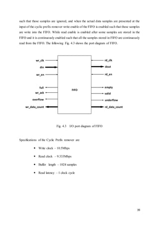
3.2.3 Down Sampler
The down sampler is the one which resample the signal at a lower sampling rate for
the processing of the signal by low data rate devices. In this project, the received signal is
sampled at a high sampling rate of 84 Mbps. But the actual data rate is 10.5 Mbps. That
means 8 consecutive samples have only one bit information. The modules such as cyclic
prefix remover, FFT process the direct data bits only, they cannot operate on up sampled
version of the signal. Hence a down sampler is used to reduce the sampling rate from 84
Mbps to actual data rate of 10.5 Mbps.
In this project the down sampler is implemented using First In First Out (FIFO) IP
Core. FIFO IP core can be operated by using either independent clocks or common clocks
for writing into FIFO and reading out from FIFO. FIFO is fully configurable using Xilinx
Core generator[22]. It supports sample depths up to 4,194,304 words each with widths from
1 to 1024 bits. It gives options selectable memory type such as block RAM, distributed
RAM, shift register or built in FIFO. It provides configurable handshake signals. Full, empty](https://image.slidesharecdn.com/finalprojectreport-150521142915-lva1-app6891/85/OFDM-based-baseband-Receiver-32-320.jpg)


![36
The cyclic extensions (either prefix or postfix) are used for the symmetry of symbol
which is useful in finding the start of the symbols. In cyclic prefix a part of the OFDM
symbol from the tail of the OFDM symbol is added in front of the OFDM symbol. In cyclic
postfix a part of the OFDM symbol from the start of the OFDM symbol is added to the end of
the OFDM symbol. Generally cyclic prefix is used, for the detection of the start of the OFDM
symbol.
In order to the cyclic prefix to be effective, the length of the cyclic prefix must be
greater than or at least equal to delay spread. Generally the length of the cyclic prefix is taken
as 1/8th or 1/4th of the OFDM symbol length. Prefixing the end of the symbol to the beginning
makes the linear convolution symbol with the channel as the circular convolution. The cyclic
prefix insertion is shown in the following Fig. 4.1.
4.2.1
Fig. 4.1 OFDM symbols with cyclic prefix insertion
4.2.1 Mathematical model of OFDM signal with cyclic prefix
Let N be the number of subcarriers in the given OFDM system. The data symbol is given by
Inverse Discrete Fourier Transform (IDFT) of the data symbol gives the OFDM
symbol. Let X’(n) is the nth subcarrier of the OFDM symbol and it is given by the following
equation.
𝒅 = [ 𝒅 𝟎, 𝒅 𝟏, 𝒅 𝟐, … . 𝒅 𝑵−𝟏] 𝑻
Cyclic
Prefix
Cyclic
PrefixSymbol S0 Symbol S1
Guard
Interval
Fade
Interval
Symbol Period
CyclicPrefix Insertion](https://image.slidesharecdn.com/finalprojectreport-150521142915-lva1-app6891/85/OFDM-based-baseband-Receiver-36-320.jpg)
![37
The OFDM symbol is given by
After insertion of cyclic prefix, the OFDM symbol is given as follows. Here L is the
length of the cyclic prefix.
Let the length of the channel impulse response is also equal to L, then the impulse
response of the channel is given by
Let y be the OFDM symbol, after convolution with the channel impulse response.
Then the OFDM symbol after convolution is given in following equation, where y(m) shows
the sample of the OFDM symbol.
The linear convolution becomes circular convolution, as x(m-l) = x’(m-l mod N) due
to the insertion of cyclic prefix. Frequency spectrum of OFDM symbol after convolution is
product of actual spectrum of OFDM symbol and the spectrum of channel impulse response.
𝑿′ = [ 𝒙( 𝟎), 𝒙( 𝟏), 𝒙( 𝟐),…. 𝒙( 𝑵 − 𝟏)] 𝑻
𝒉 = [ 𝒉 𝟎, 𝒉 𝟏, 𝒉 𝟐,… . 𝒉 𝑳−𝟏] 𝑻
𝒚( 𝒎) = ∑ 𝒉(𝒍)𝒙(𝒎− 𝒍)
𝑳−𝟏
𝒍=𝟎
; 𝑳 − 𝟏 ≤ 𝒎 ≤ 𝑵 − 𝟏
𝒀( 𝒌) = 𝑿(𝒌)𝑯(𝒌)
𝑿 = [ 𝒙( 𝑵 − 𝑳 + 𝟏), 𝒙( 𝑵 − 𝑳 + 𝟐),… . 𝒙( 𝑵 − 𝟐), 𝒙( 𝑵 − 𝟏), 𝒙( 𝟎), 𝒙( 𝟏), 𝒙( 𝟐),… . 𝒙( 𝑵 − 𝟏)] 𝑻
𝑿′(𝒏) = ∑ 𝒅(𝒏)𝒆
𝒋𝒘𝒏𝒌
𝑵
𝑵−𝟏
𝒌=𝟎
; 𝟎 ≤ 𝒏 ≤ 𝑵 − 𝟏](https://image.slidesharecdn.com/finalprojectreport-150521142915-lva1-app6891/85/OFDM-based-baseband-Receiver-37-320.jpg)


![43
4.3.2 Reasonfor usage of FFT in OFDM Receiverfor Demodulation
The generation of orthogonal carriers using number of local oscillators is not a simple
task. Even if there is a small change in frequency the orthogonality of subcarriers is lost. And
the usage multiple local oscillators and making sure that they stable at the orthogonal
frequencies makes the OFDM system more complex. Fortunately the DFT basis functions are
orthogonality i.e. any two coefficients (twiddle factors) of DFT are orthogonal. This is the
basic property of the DFT that makes it, to use in generation of orthogonal frequency carriers
in OFDM. As DFT is implemented simply by FFT, FFT is used in OFDM system. The
orthogonality of the twiddle factors is shown in the following equation.
In transmitter, the digital data bits are mapped to amplitude and phase values and
placed at correct locations in frequency spectrum. This signal has to be modulated using
number of orthogonal subcarriers and it is in frequency domain. As IFFT converts the
frequency domain signal to time domain signal, IFFT is used to modulate this signal.
At the receiver, the received signal is in time domain so FFT is used to demodulate
the signal. FFT converts the time domain signal into frequency domain signal. After
demodulation the amplitude and phase of the subcarriers are mapped and demodulated to
digital data bits.
4.3.3 Features of FFT IP Core
In this project, FFT block is implemented using the FFT IP Core. FFT IP core[23]
computes N-point forward or inverse DFT where N = 2m, m= 3 to 16. It provides run time
configurable forward and inverse complex FFT. It accepts data and phase factor precision of
8 to 34 bits. The total memory is on chip using either block RAM or distributed RAM. The
input data must be in natural order and the output data can be in either natural or bit reversal
order. It provides three arithmetical options for computation of FFT.
∑ 𝑾 𝑵
𝒏𝒌′
𝑾 𝑵
𝒏𝒌
= 𝑵𝜹 𝑵(𝒌 − 𝒌′
)
𝑵−𝟏
𝒏=𝟎](https://image.slidesharecdn.com/finalprojectreport-150521142915-lva1-app6891/85/OFDM-based-baseband-Receiver-43-320.jpg)


![53
The advantage of OFDM is that the frequency selective fading becomes flat fading for
the subcarriers, as the total bandwidth of the signal is divided into number of sub bands. So
channel estimation becomes simpler than any other single carrier modulation techniques.
5.2.1 Different Techniques for Channel Estimation
For coherent detection of information symbols, the channel state information has to be
found accurately and promptly. There are number of techniques for channel estimation.
Broadly they are divided into three groups. They are
i. Non data aided channel estimation
ii. Data aided channel estimation
iii. Semi data aided channel estimation
i. Non Data Aided Channel Estimation
In non data aided channel estimation, no additional data is transmitted along the user
data for the channel estimation. The channel state information is estimated using some of
transmitted signal properties and statistical information of channel. It requires the long data
records for estimation channel characteristics. It is applicable only to slow fading channels. It
is not applicable to fast fading channels. It is also known as blind channel estimation. The
advantage of this technique is, there is no overhead loss but the estimation is poor.
ii. Data Aided Channel Estimation
It is also known as training/pilot based channel estimation. In this technique, training
symbols or pilot bits that are known prior to the receiver are multiplexed with the user data
bits for the channel estimation[18]. This is the better technique for the channel estimation
because it requires no long data records for the channel estimation. It can be applicable to the
fast time varying channels also. It is complex to implement, but the estimation is reliable.](https://image.slidesharecdn.com/finalprojectreport-150521142915-lva1-app6891/85/OFDM-based-baseband-Receiver-53-320.jpg)


![64
Port Name Direction Description
X_IN Input X component of input sample
Y_IN Input Y component of input sample
ND Input New sample on input ports (Active high)
CE Input Clock enable (Active high)
CLK Input Rising edge Clock
PHASE_OUT Output Phase component of the output sample.
RFD Output Ready for new data sample (Active high)
RDY Output New output data is ready (Active high)
Table. 5.2 I/O port description of Cordic
The above Table. 5.2 describes the I/O ports of the Cordic. Cordic[24] accepts the real
and imaginary components of a complex signal and it gives the phase of the complex signal.
Knowing phase angle of a complex signal (symbol) is nothing but knowing about the
quadrant (Cartesian quadrant) in which the symbol falls. If the quadrant of the symbol is
known then the corresponding digital data bits are assigned using VHDL coding[15]. Thus
QPSK demapper is implemented successfully using Cordic IP core.
5.7 Result
The functioning of pilot extractor is tested using the pilot inserter. The output of the
pilot inserter is fed as the input to pilot extractor. In this project the pilot are inserted at the
subcarriers numbered 7, 14, 21, 28, 35, 42, 49, and 56. And the subcarriers numbered 0, 1, 2,
3, 60, 61, 62, and 63 are used as nulls. That means no data is transmitted on these sub
carriers. The pilot inserter transfers the user data bits when the subcarriers other than
mentioned above come and it inserts the pilot bits when pilot subcarriers comes and transfer
zeros when null subcarriers come. The designed pilot extractor reads the data when the user
data subcarriers are present and it transfer the data to data output and reads the data of pilot
subcarriers and transfers the data to pilot data output and when null subcarriers come it](https://image.slidesharecdn.com/finalprojectreport-150521142915-lva1-app6891/85/OFDM-based-baseband-Receiver-64-320.jpg)


![70
Fig. 6.2 VHDL simulation output of testing of OFDM based baseband receiver with OFDM
based baseband transmitter giving zero BER
6.4 Hardware Implementation of OFDM BasedBaseband Receiver
After successful design and integration of OFDM based baseband Receiver modules,
it has to be implemented on Spartan-3 (XC3S5000) FPGA. After successful simulation of the
design, the design is synthesized and programming file is generated using Xilinx ISE Design
Suite 13.2. The FPGA board is connected to the computer having the software ChipScope Pro
Tool using the Xilinx Platform Cable USB II and JTAG. The generated programming file is
dumped on to the FPGA using ChipScope Pro Tool.
6.4.1 Spartan-3 FPGA
The Spartan -3 family FPGAs[25] enhanced with more logic resources, more number
of I/O ports, increased internal RAM, improved clock management functions. These Spartan-
3 FPGAs have advanced process technology and deliver more functionality, and setting new
standards in programmable logic industry.](https://image.slidesharecdn.com/finalprojectreport-150521142915-lva1-app6891/85/OFDM-based-baseband-Receiver-70-320.jpg)


![73
ii. The combinational path length has to be reduced such that the combinational path
delay is less than the clock period. The combinational path length can be reduced by
inserting sequential elements such as flip-flops, buffers in the combinational path.
After removal all problems occurred in hardware implementation and successful
implementation of the design on Spartan-3 FPGA. The Digital to Analog Converter
(DAC5682Z) is configured to the FPGA and the output of the DAC is given to spectrum
analyzer HP8593E. The spectrums of the signals at different stages are observed.
6.4.5 DAC5682Z
. DAC5682Z[26] is a dual channel 16 – bit, 1.0 GSPS digital to analog converter with
wideband data input, integrated 2x/4x interpolation filters, on-board clock multiplier and
internal voltage reference. The DAC5682Z offers superior linearity, noise, crosstalk and PLL
phase noise performance.
6.4.6 Hardware Setup for Testing of OFDM BasedBaseband Receiver
The above Fig. 6.3 shows the hardware setup for testing the OFDM based baseband
Receiver for wireless radio. The computer, which has ChipScope Pro tool, is connected to the
FPGA board using the Xilinx Platform Cable USB II and JTAG. The FPGA board is
configured using ChipScope Pro tool. The regulated DC power supply is used for powering
the FPGA board. The board requires voltage of 5V and current of 0.5-0.8A. The output of the
DAC is connected to spectrum analyzer through SMA connector. The spectrums of signals at
different stages are observed. Thus the OFDM based baseband Receiver for wireless radio
application is implemented successfully.](https://image.slidesharecdn.com/finalprojectreport-150521142915-lva1-app6891/85/OFDM-based-baseband-Receiver-73-320.jpg)


![78
There are number algorithms proposed in literature for carrier frequency, phase offset
estimation and clock frequency offset and delay estimation. In this project, some of the
carrier frequency offset estimation techniques are studied and three of them are implemented
in MATLAB. They are
1. Maximum Likelihood (ML) Estimation
2. Modified Van de Beek Algorithm
3. Schmidl and Cox’s Algorithm
7.4 Maximum Likelihood Estimation
It is proposed by Van de Beek. In this analysis, the channel is assumed to be non
dispersive, the transmitted signal s(k) is effected by complex additive white Gaussian noise
(AWGN) n(k) only. Here at the receiver two uncertainties are considered. One is the
uncertainty in the arrival time of the OFDM symbol and other is the uncertainty in the carrier
frequency[16]. The first uncertainty is modeled as a delay in channel impulse response δ(k-
θ), where θ is the integer valued unknown arrival time of a symbol. The latter is modeled as
complex multiplicative distortion of the received signal in time domain and it is given by
(𝑒
𝑗2𝜋∈𝑘
𝑁 ) , where ε denotes the carrier frequency offset normalized by inter carrier spacing.
The received signal with these two uncertainties is given by
𝒓( 𝒌) = 𝒔( 𝒌 − 𝜽) 𝒆
𝒋𝟐𝝅∈𝒌
𝑵 + 𝒏(𝒌)
In this estimation 2N+L consecutive samples of received signal are observed. Where
N is the number of subcarriers and L is the length of the cyclic prefix. The OFDM symbol
consists of total N+L samples. The likelihood function is given by
𝜦( 𝜽, ∈) = |𝜸( 𝜽)| 𝐜𝐨𝐬(𝟐𝝅𝝐 + ⦟ 𝜸( 𝜽))− 𝝆∅(𝜽)](https://image.slidesharecdn.com/finalprojectreport-150521142915-lva1-app6891/85/OFDM-based-baseband-Receiver-78-320.jpg)


![81
Fig. 7.3 Output of timing and frequency offset estimation of OFDM symbols using ML
estimation (Peaks in top plot indicate the start of OFDM symbols, bottom plot gives the
corresponding frequency offset)
7.5 Modified Van de Beek Algorithm
In this algorithm preamble pattern is used for carrier frequency offset estimation. The
preamble used in this algorithm consists of one full OFDM symbol of 64 samples in which 16
samples are repeated for four times[19]. This algorithm consists of two branches, one for
calculating the energy and other for finding correlation. The correlation with delay 16 (ms3)
is used to calculate the phase which is used to estimate the carrier frequency offset. The phase
of ms3, when the magnitude of difference between ms1 and ms2 reaches a maximum
(Argmax) gives the carrier frequency offset. The operation ensures that the carrier frequency
offset estimation is done at best time. The following Fig. 7.4 shows the data flow diagram of
modified Van de Beek algorithm and preamble format.](https://image.slidesharecdn.com/finalprojectreport-150521142915-lva1-app6891/85/OFDM-based-baseband-Receiver-81-320.jpg)

![83
Fig. 7.5 Output of timing and frequency offset estimation of OFDM symbols using modified
Van de Beek algorithm (Peaks in top plot indicate the start of OFDM symbols, bottom plot
gives the corresponding frequency offset)
7.6 Schmidl and Cox Algorithm
The preamble used in this algorithm consists of one full OFDM symbol of 64 samples
in which 32 samples are repeated for two times and is shown in the following figure. The
preamble structure and data flow diagram of Schmidl and Cox Algorithm[17] is shown in the
following Fig. 7.6.](https://image.slidesharecdn.com/finalprojectreport-150521142915-lva1-app6891/85/OFDM-based-baseband-Receiver-83-320.jpg)


![99
References
[1] M Jose Canet, Felip Vicedo, Vicenc Almenar, and Javier Valls, “FPGA
Implementation of an IF Transceiver for OFDM Based WLAN”, IEEE workshop on
Signal Processing Systems, Oct. 2004, pp. 227-232.
[2] Christoph Sonntag, “Orthogonal Frequency Division Multiplexing (OFDM)
implementation as part of a Software Defined Radio (SDR) environment”, M.S.
thesis, Dept. Elect. & Electron. Eng., Univ. Stellenbosch, Matieland, South Africa,
Dec. 2005.
[3] Khaled Sobaihi, Akram Hammoudeh, and David Scammell, “FPGA Implementation
of OFDM Transceiver for a 60GHz Wireless Mobile Radio System”, International
Conference on Reconfigurable Computing and FPGAs (ReConFig), Quintana Roo,
Mexico, Dec. 2010, pp. 185-189.
[4] Lenin Gopal, Daniel Wong Sing Tze, and Nur Zawanah Ishak, “Design of an FPGA-
Based OFDM Transceiver for DVB-T Standard”, IEEE International Conference on
Computer Science and Automation Engineering (CSAE), Shanghai, China, vol. 3,
Jun. 2011, pp. 193-197.
[5] Yin-Tsung Hwang, Sung-Jun Tsai, and Yi-Yo Chen, “Design and Implementation of
an Optical OFDM Baseband Receiver in FPGA”, International Symposium on VLSI
Design, Automation, and Test (VLSI-DAT), Hsinchu, China, Apr. 2012, pp. 1-4.
[6] Shaminder Kaur and Rajesh Mehra, “FPGA Implementation of OFDM Transceiver
using FFT Algorithm”, International Journal of Engineering Science and Technology
(IJEST), Vol. 4, No.04, Apr. 2012, pp. 1532-1537.
[7] Michael Mefenza and Christophe Bobda, “FPGA Implementation of Subcarrier Index
Modulation OFDM Transceiver”, IEEE 27th International Symposium on Parallel &
Distributed Processing Workshops and PhD Forum (IPDPSW), Cambridge, MA, May
2013, pp. 268-272.
[8] Akash Mecwan and Dhaval Shah, “Implementation of OFDM Transceiver on FPGA”,
Nirma University International Conference on Engineering (NUiCONE), Ahmadabad,
India, Nov. 2013, pp. 1-5.](https://image.slidesharecdn.com/finalprojectreport-150521142915-lva1-app6891/85/OFDM-based-baseband-Receiver-99-320.jpg)
![100
[9] P. Sadhasivam and Dr. M. Manikandan, “Design And Analysis Of OFDM
Transceiver With Novel Architecture”, International Conference on Current Trends in
Engineering and Technology (ICCTET), Coimbatore, India, July 3, 2013, pp. 248-
251.
[10] Nasreen Mev and Brig. R.M. Khaire, “Implementation of OFDM Transmitter and
Receiver Using FPGA”, International Journal of Soft Computing and Engineering
(IJSCE), Vol. 3, No. 3, July 2013, pp. 199-202.
[11] Tirumala Rao Pechetty and Mohith Vemulapalli, “An Implementation of OFDM
Transmitter and Receiver on Reconfigurable Platforms”, International Journal of
Advanced Research in Electrical, Electronics and Instrumentation Engineering
(IJAREEIE), Vol. 2, No. 11, Nov. 2013.
[12] Ramjee Prasad, “OFDM for Wireless Communications Systems”, Artech House,
2004.
[13] K. Fazel and S. Kaiser, “Multi- Carrier and Spread Spectrum Systems- From OFDM
and MC-CDMA to LTE and WiMAX”, 2nd Edition, Wiley, 2008.
[14] L. Hanzo and T. Keller, “OFDM and MC CDMA-A Primer”, IEEE press, Wiley,
2006.
[15] J. Bhasker, “A VHDL Primer”, 3rd Ed., Prentice Hall, 1998.
[16] Jan-Jaap van de Beek and Magnus Sandell, “ML Estimation of time and frequency
offset in OFDM systems”, IEEE transactions on signal processing, vol. 45, No.7, July
1997, pp. 1800-1805.
[17] Timothy M. Schmidl and Donald C. Cox, “Robust Frequency and Timing
Synchronization for OFDM”, IEEE Transactions on Communications, Vol. 45, No.
12, Dec. 1997, pp. 1613-1621.
[18] Kala Praveen Bagadi and Susmita Das, “MIMO-OFDM Channel Estimation using
Pilot Carries”, International Journal of Computer Applications, vol 2, No.3, May
2010, pp. 81-88.
[19] Implementing WiMAX OFDM Timing and Frequency Offset Estimation in Lattice
FPGAs, Lattice Semiconductor Corporation, Oregon, USA, Nov. 2005.
[20] LogiCORE IP Multiplier v11.2, Xilinx product specification, March 1, 2011.
[21] LogiCORE IP FIFO Generator v8.2, Xilinx product specification, March 1, 2011.
[22] IP LogiCORE FIR Compiler v5.0, Xilinx product specification, March 1, 2011.](https://image.slidesharecdn.com/finalprojectreport-150521142915-lva1-app6891/85/OFDM-based-baseband-Receiver-100-320.jpg)
![101
[23] LogiCORE IP Fast Fourier Transform v7.1, Xilinx product specification, March 1,
2011.
[24] LogiCORE IP CORDIC v4.0, Xilinx product specification, March 1, 2011.
[25] Spartan-3 FPGA Family Data Sheet, Xilinx product specification, June 27, 2013.
[26] 16-BIT 1.0 GSPS 2x-4x Interpolating Dual-Channel Digital-to-Analog Converter
(DAC5682Z), Texas Instruments, Aug. 2012.](https://image.slidesharecdn.com/finalprojectreport-150521142915-lva1-app6891/85/OFDM-based-baseband-Receiver-101-320.jpg)

The document provides an overview of Orthogonal Frequency Division Multiplexing (OFDM), detailing its advantages, applications, and related technologies. It discusses the simplicity of channel equalization in OFDM systems, the importance of orthogonality among subcarriers, and various implementations and simulations of OFDM systems on different platforms. The focus of the present project is on developing an OFDM based baseband receiver designed for industrial requirements, with specifications detailing data rates, subcarrier usage, and modulation techniques.