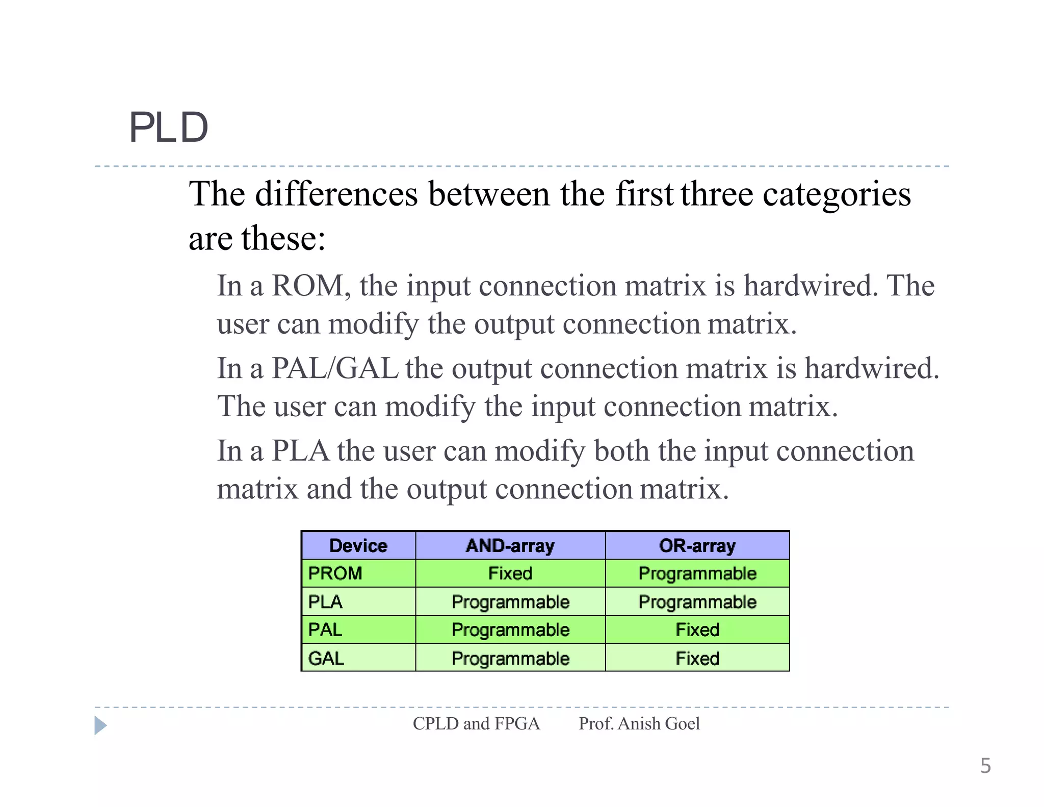
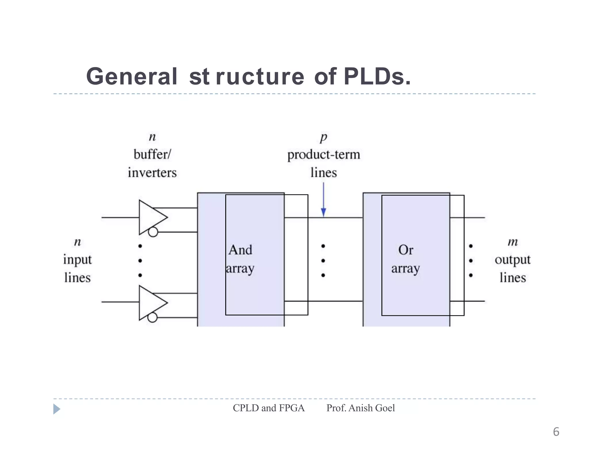
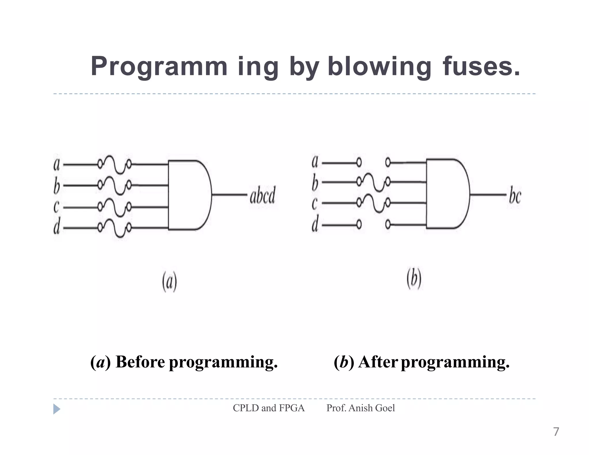
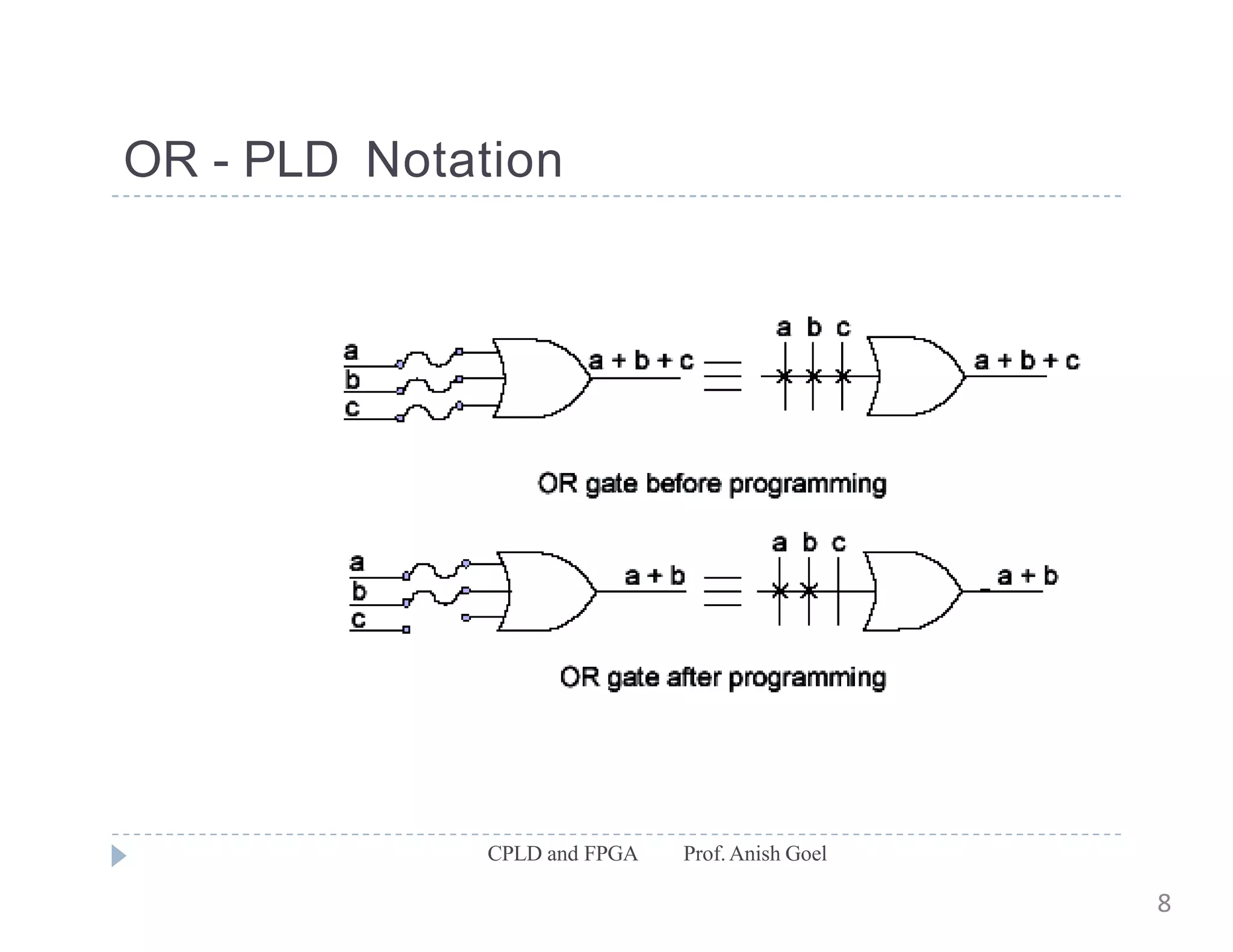
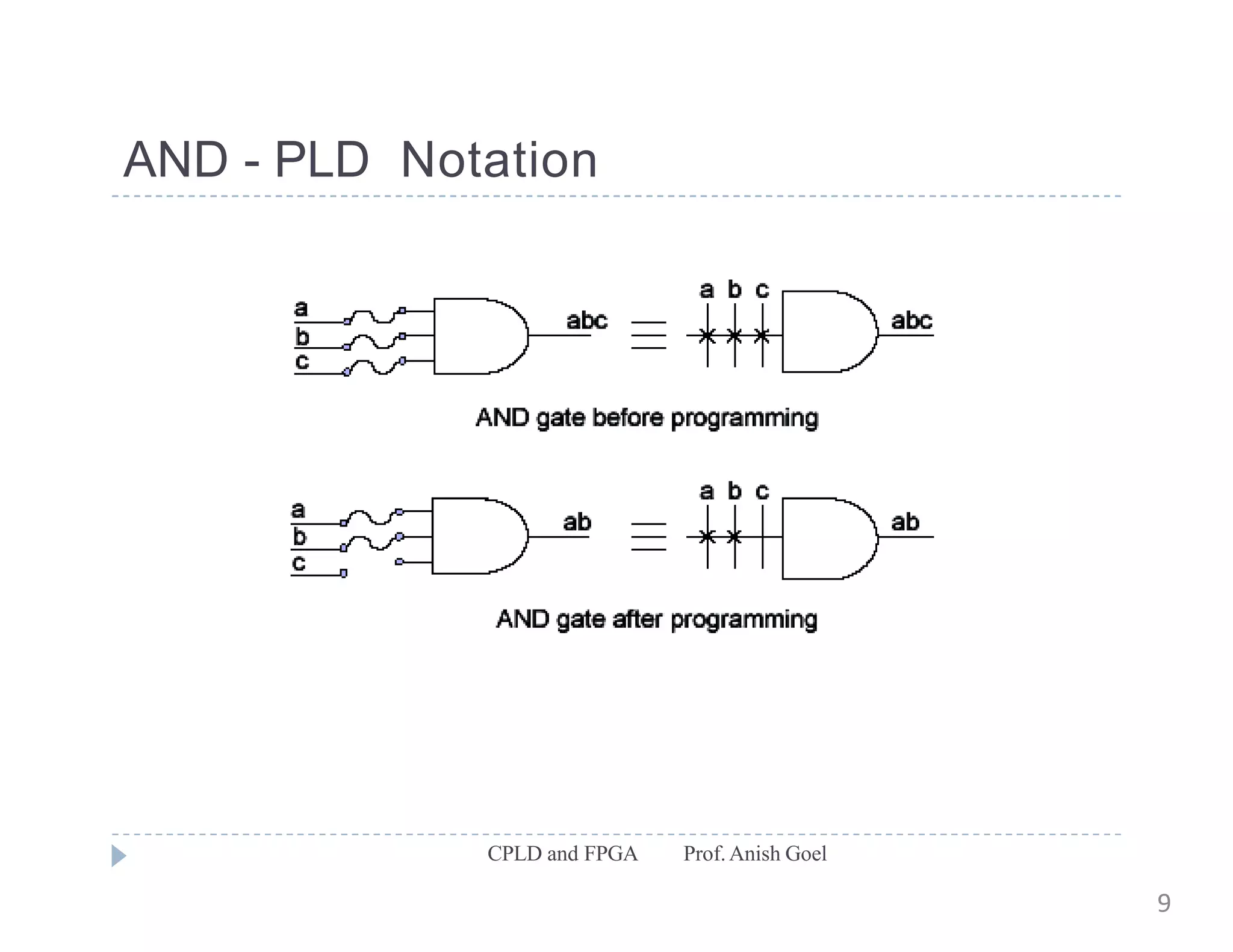
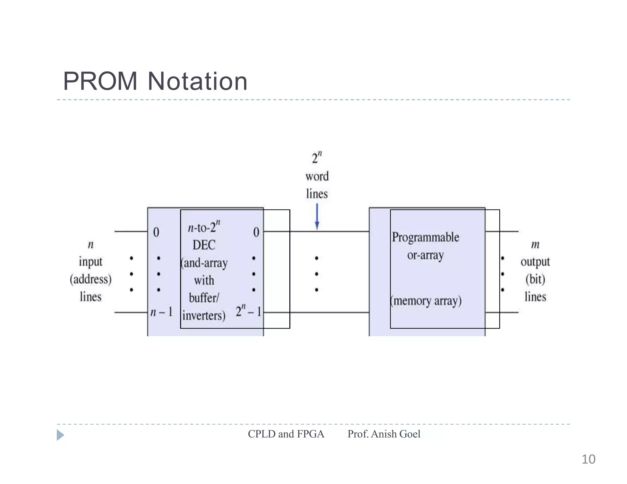
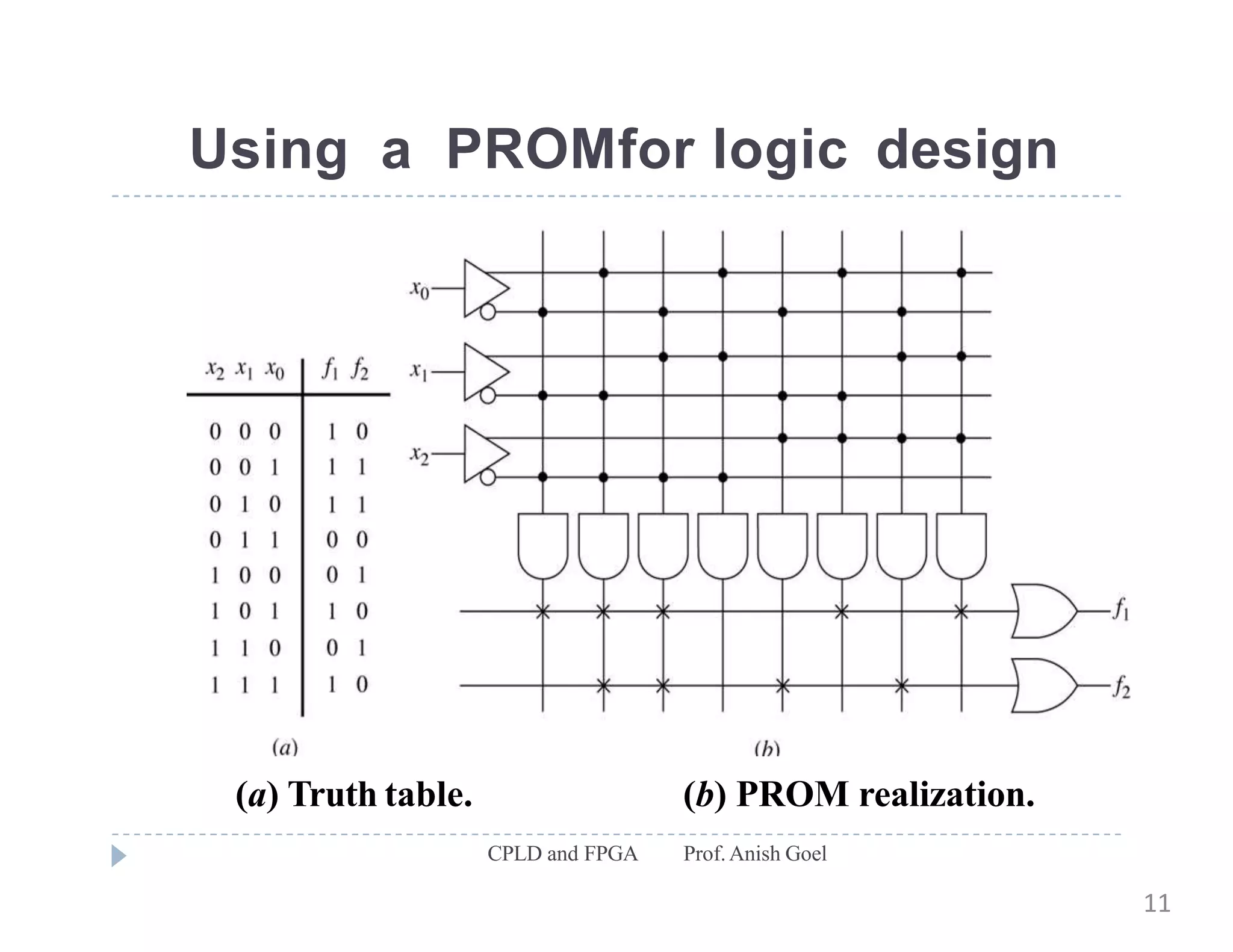
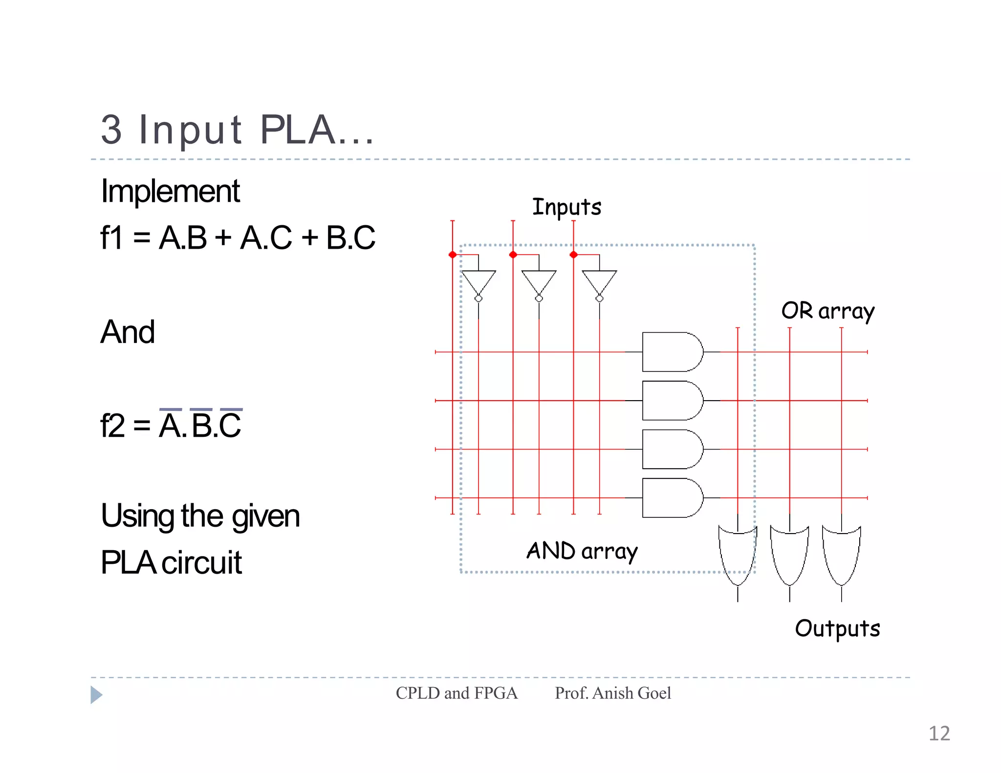
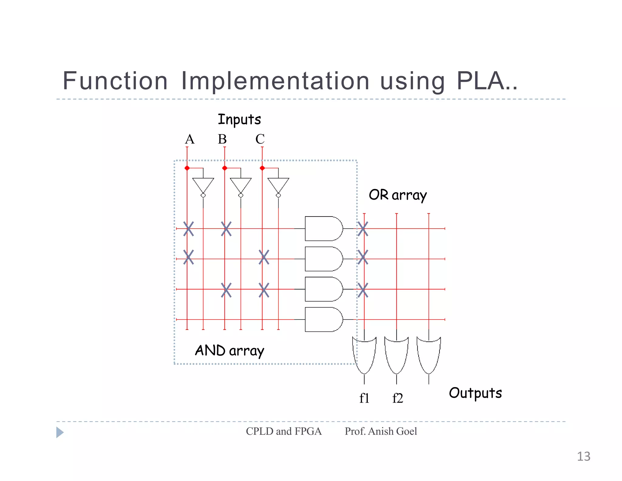
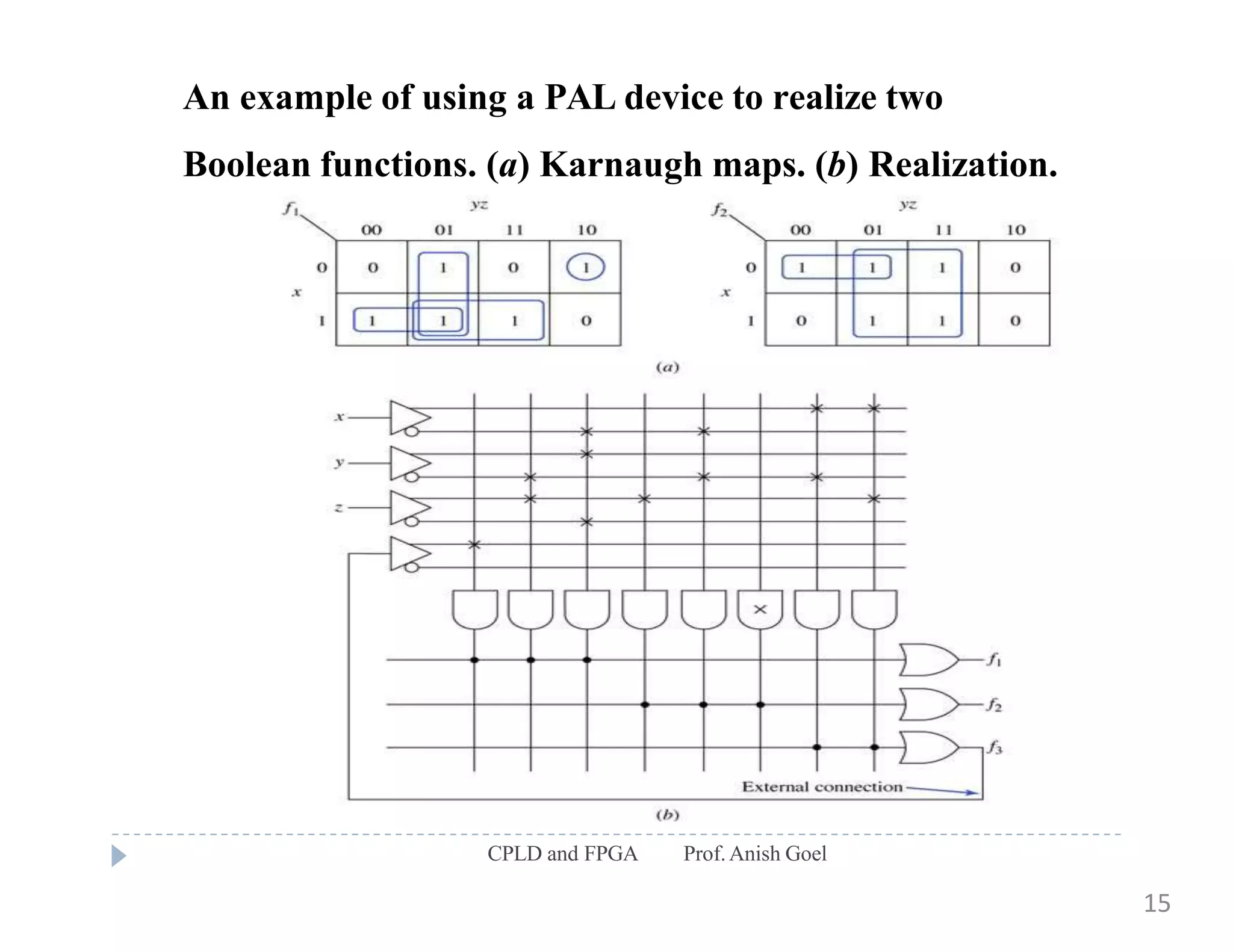
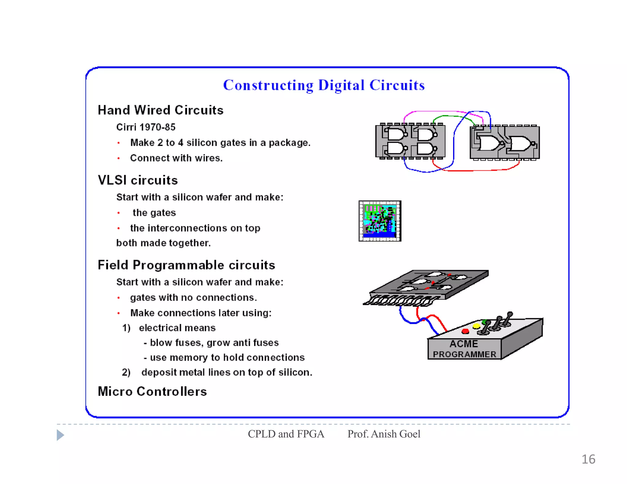
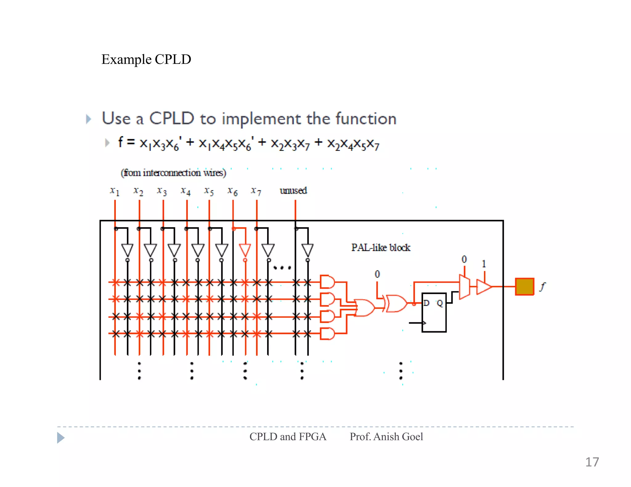
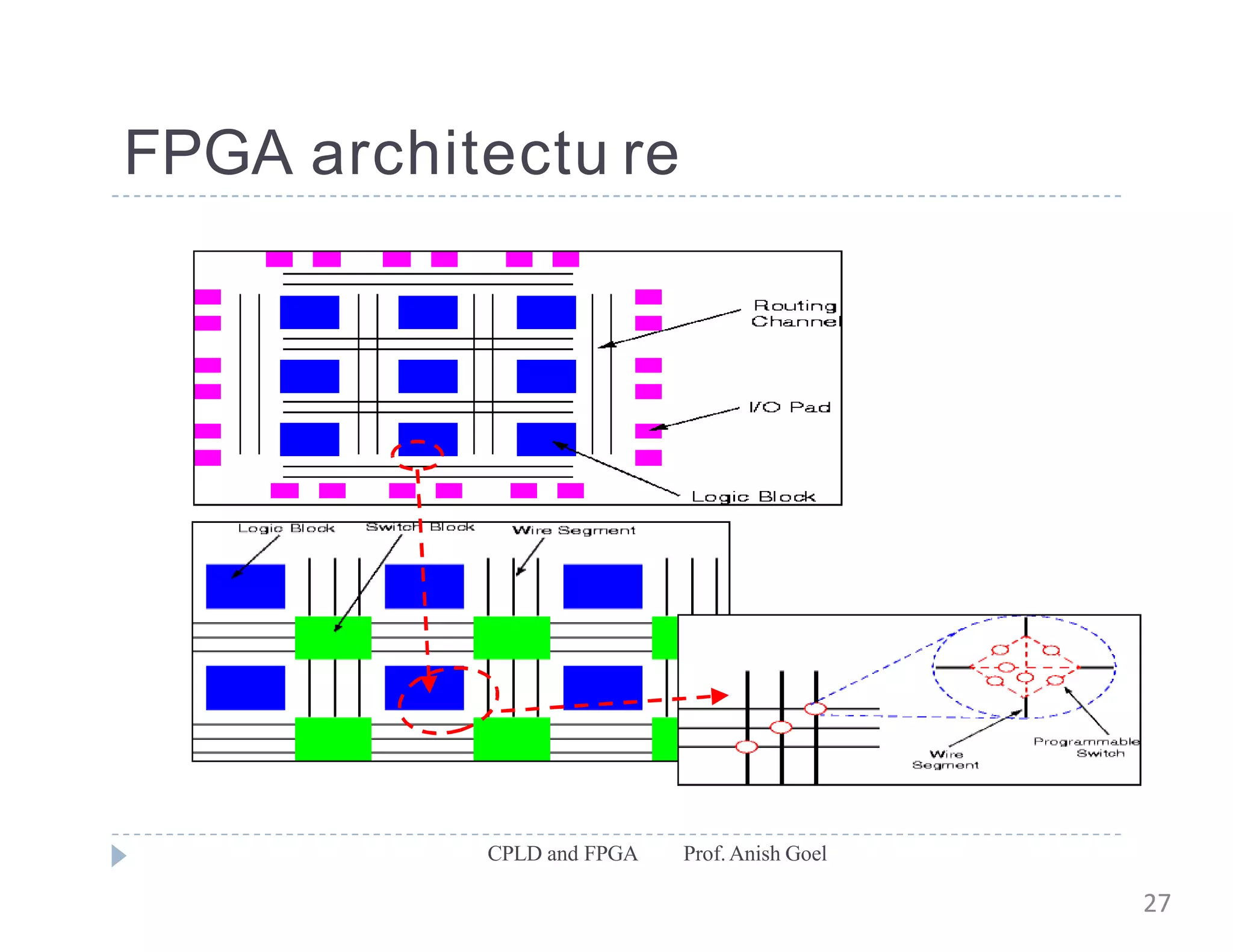
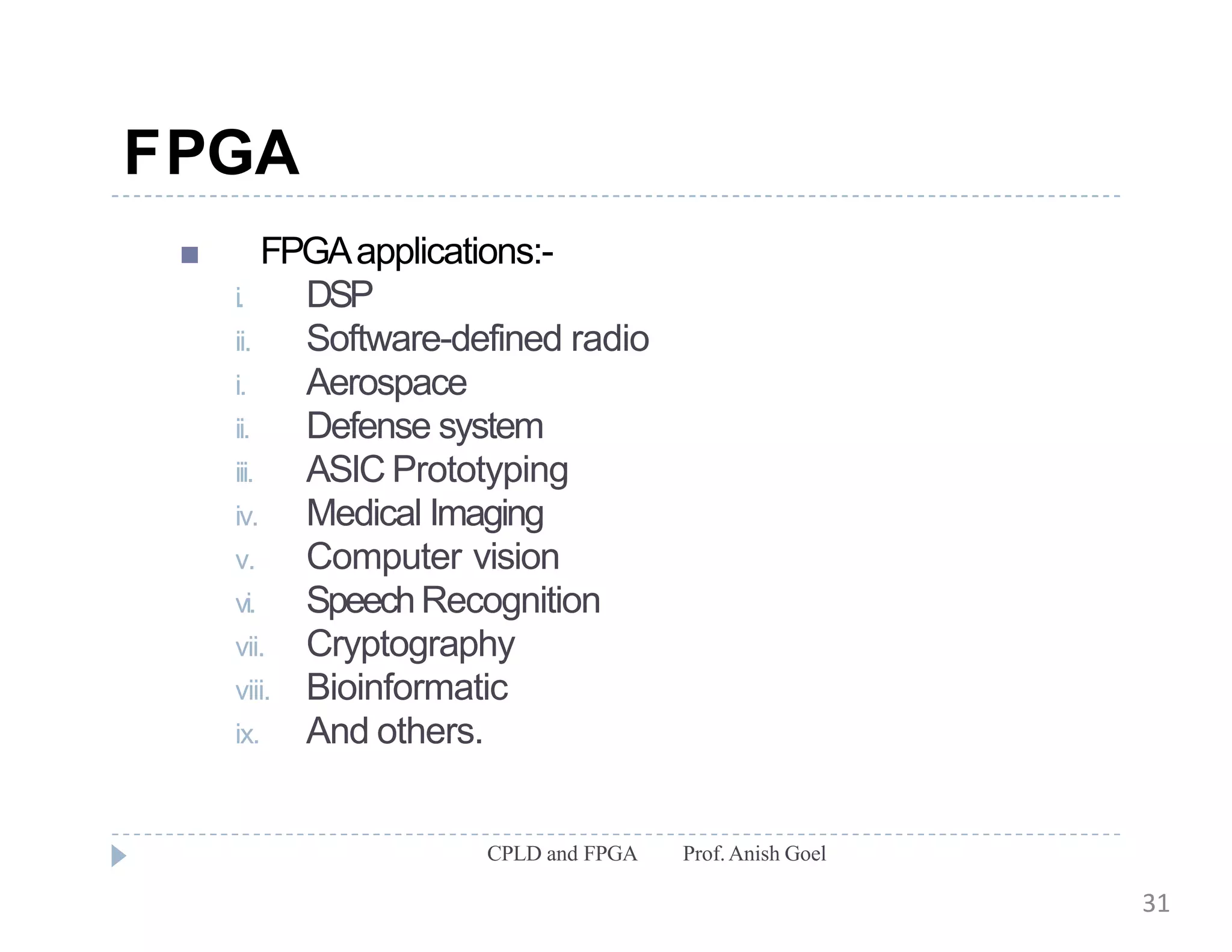
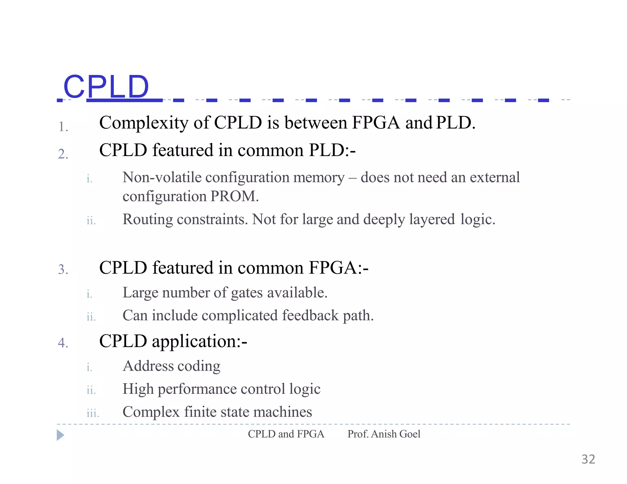
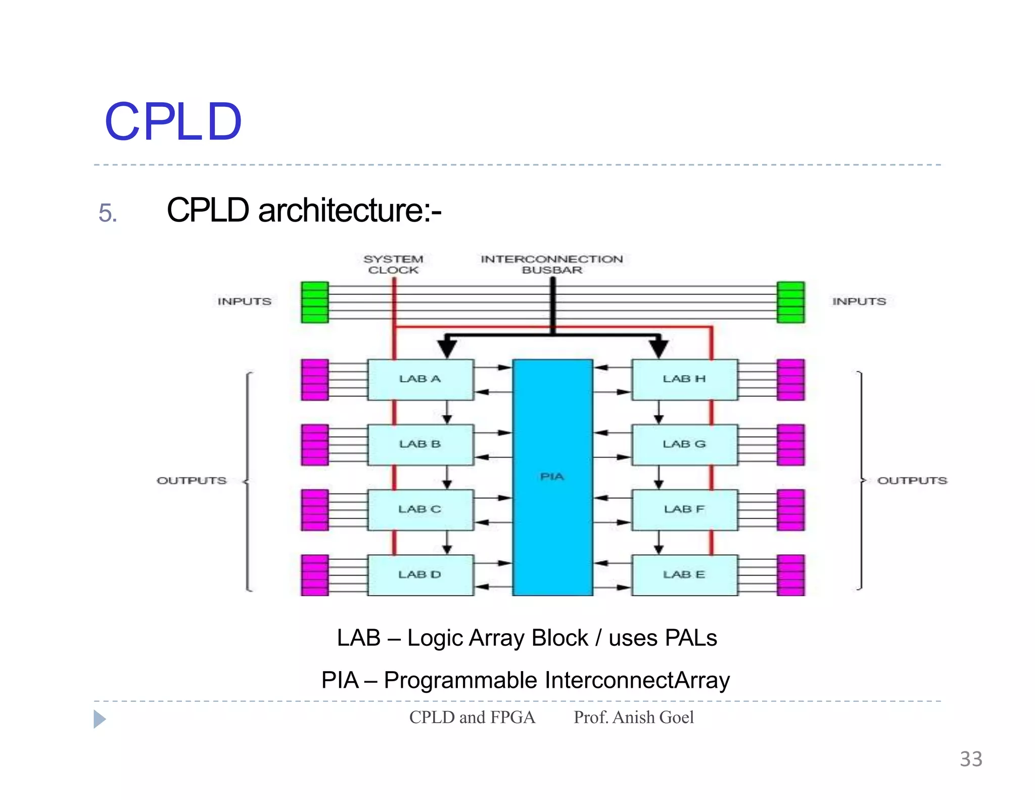
2. PLD
CPLD and FPGA Prof.Anish Goel
Problems by Using Basic Gates
Many components on PCB:
As no. of components rise, nodes interconnection complexity
grow exponentially
Growth in interconnection will cause increase in interference,
PCB size, PCB design cost, and manufacturing time
2
3. PLD
CPLD and FPGA Prof.Anish Goel
The purpose of a PLD device is to permit elaboratedigital logic
designs to be implemented by the user in a singledevice.
Can be erased electrically and reprogrammed with anew design,
making them very well suited for academic and prototyping
Types of Programmable Logic Devices
SPLDs (Simple Programmable Logic Devices)
ROM (Read-Only Memory)
PLA (Programmable LogicArray)
PAL(Programmable Array Logic)
GAL (Generic Array Logic)
CPLD (Complex Programmable Logic Device)
FPGA (Field-Programmable GateArray)
3
4. PLD
CPLD and FPGA Prof.Anish Goel
The first three varieties are quite similar to eachother:
They all have an input connection matrix, which connects the
inputs of the device to an array ofAND-gates.
They all have an output connection matrix, which connect
the outputs of the AND-gates to the inputs of OR-gates
which drive the outputs of the device.
The gate array is significantly different andwill be
described later.
4
5. PLD
The differences between the first three categories
are these:
In a ROM, the input connection matrix is hardwired. The
user can modify the output connection matrix.
In a PAL/GAL the output connection matrix is hardwired.
The user can modify the input connection matrix.
In a PLA the user can modify both the input connection
matrix and the output connection matrix.
CPLD and FPGA Prof.Anish Goel
5
25. FPGA AND CPLD
CPLD and FPGA Prof.Anish Goel
1. FPGA- Field-Programmable Gate Array.
2. CPLD- Complex ProgrammableLogic Device
3. FPGAandCPLDis an advance PLD.
4. Support thousands of gatewhere asPLDonly
support hundreds of gates.
25
26. What is an FPGA?
CPLD and FPGA Prof.Anish Goel
Before the advent of programmable logic, custom logic circuits were built at
the board level using standard components, or at the gate level in expensive
application-specific (custom) integrated circuits.
FPGA is an integrated circuit that contains many (64 to over 10,000)
identical logic cells that can be viewed as standard components.Each logic
cell can independently take on any one of a limited set of personalities.
Individual cells are interconnected by a matrix of wires and programmable
switches. A user's design is implemented by specifying the simple logic
function for each cell and selectively closing the switches in the
interconnect matrix.
Array of logic cells and interconnect form a fabric of basic building blocks
for logic circuits. Complex designs are created by combining these basic
blocks to create the desired circuit
26
28. What does a logic cell do?
CPLD and FPGA Prof.Anish Goel
The logic cell architecture varies between different device families.
Each logic cell combines a few binary inputs (typically between 3 and 10)
to one or two outputs according to a Boolean logic function specified in the
user program .
In most families, the user also has the option of registering the
combinatorial output of the cell, so that clocked logic can be easily
implemented.
Cell's combinatorial logic may be physically implemented as a small look-
up table memory (LUT) or as a set of multiplexers and gates.
LUT devices tend to be a bit more flexible and provide more inputs per cell
than multiplexer cells at the expense of propagation delay.
28
29. what does 'Field Programmable' mean?
CPLD and FPGA Prof.Anish Goel
Field Programmable means that the FPGA's function is defined by a user's
program rather than by the manufacturer of the device.
A typical integrated circuit performs a particular function defined at the time
of manufacture.In contrast, the FPGA's function is defined by a program
written by someone other than the device manufacturer.
Depending on the particular device, the program is either'burned'
in permanently or semi-permanently as part of a board assembly process, or
is loaded from an external memory each time the device is powered up.
This user programmability gives the user access to complex integrated
designs without the high engineering costs associated with application
specific integrated circuits.
29
30. How are FPGA programs created?
CPLD and FPGA Prof.Anish Goel
Individually defining the many switch connections and cell logic functions
would be a daunting task.
This task is handled by special software.The software translates a user's
schematic diagrams or textual hardware description language code then
places and routes the translated design.
Most of the software packages have hooks to allow the user to influence
implementation, placement and routing to obtain better performance and
utilization of the device.
Libraries of more complex function macros (eg. adders) further simplify the
design process by providing common circuits that are already optimized for
speed or area.
30
31. FPGA
CPLD and FPGA Prof.Anish Goel
FPGAapplications:-
i. DSP
ii. Software-defined radio
i. Aerospace
ii. Defense system
iii. ASIC Prototyping
iv. Medical Imaging
v. Computer vision
vi. SpeechRecognition
vii. Cryptography
viii. Bioinformatic
ix. And others.
31
32. CPLD
CPLD and FPGA Prof.Anish Goel
1.
2.
i.
ii.
Complexity of CPLD is between FPGA and PLD.
CPLD featured in common PLD:-
Non-volatile configuration memory – does not need an external
configuration PROM.
Routing constraints. Not for large and deeply layered logic.
3.
i.
ii.
4.
i.
ii.
CPLD featured in common FPGA:-
Large number of gates available.
Can include complicated feedback path.
CPLD application:-
Address coding
High performance control logic
iii. Complex finite state machines
32