SlideShare a Scribd company logo
1 of 17
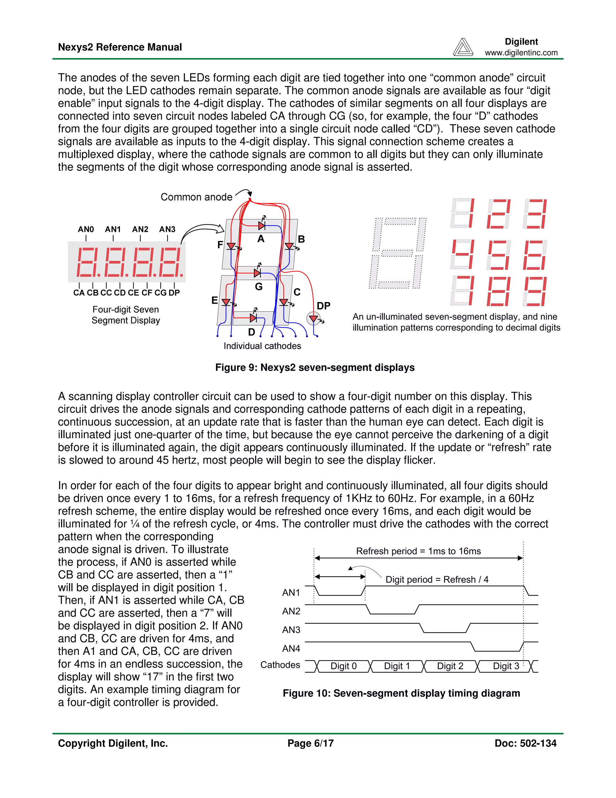
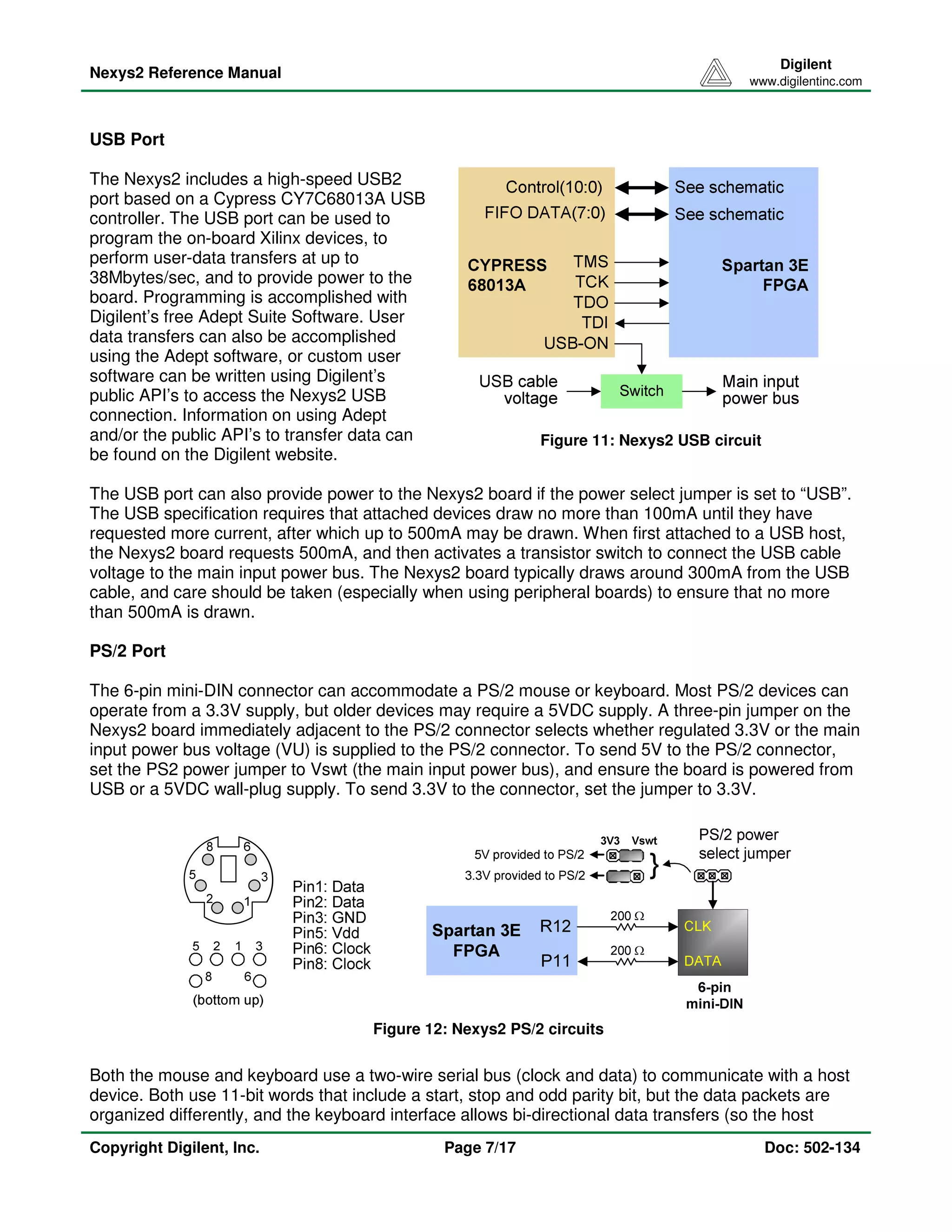
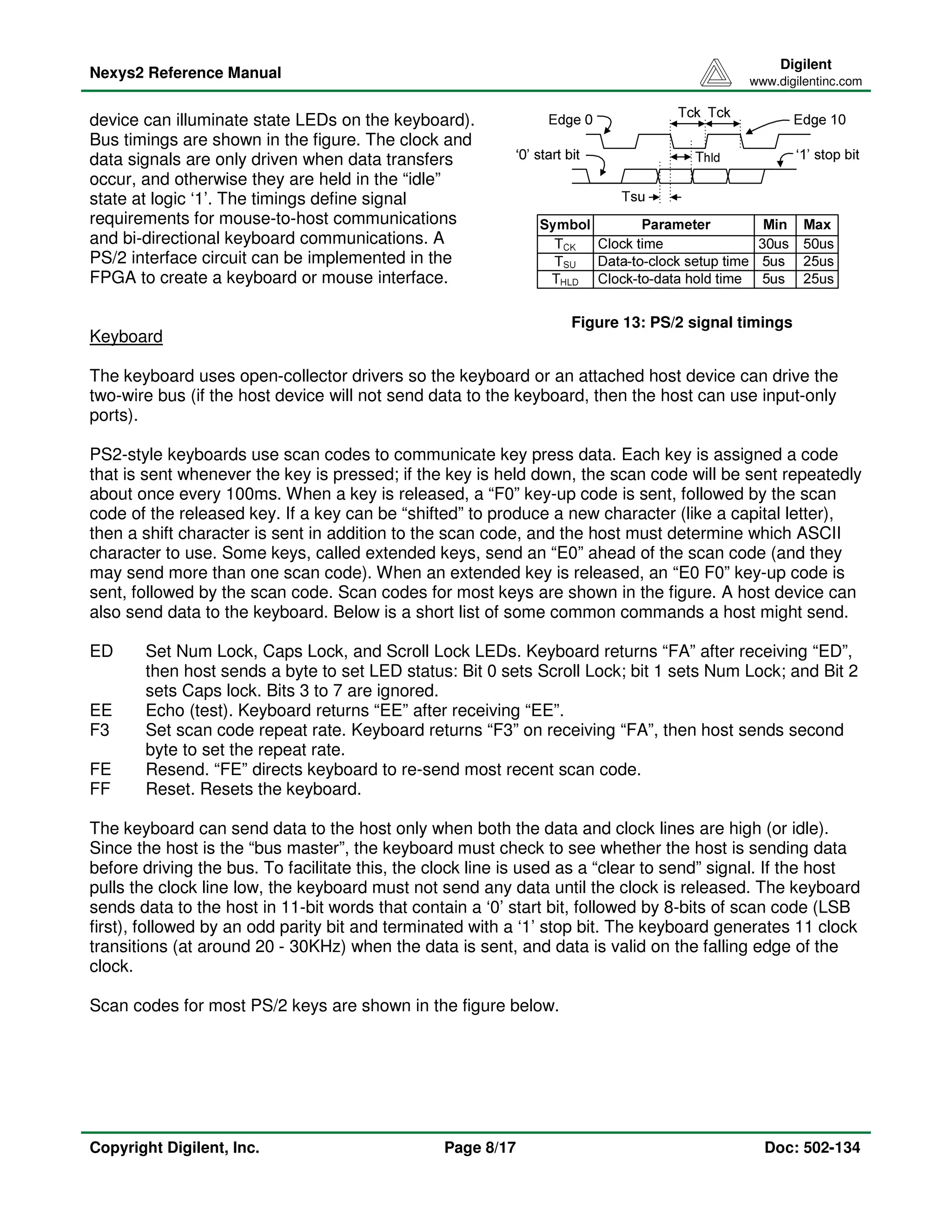
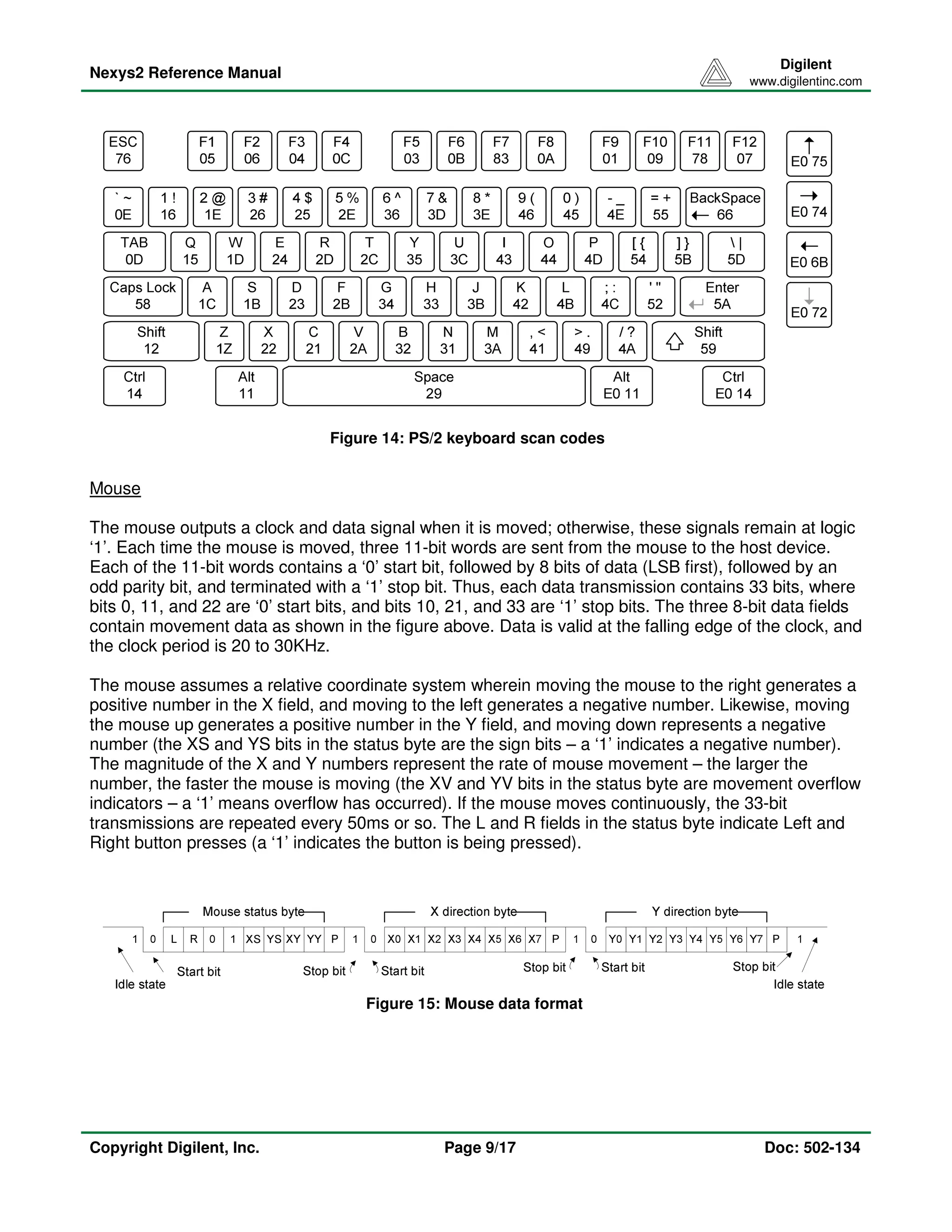
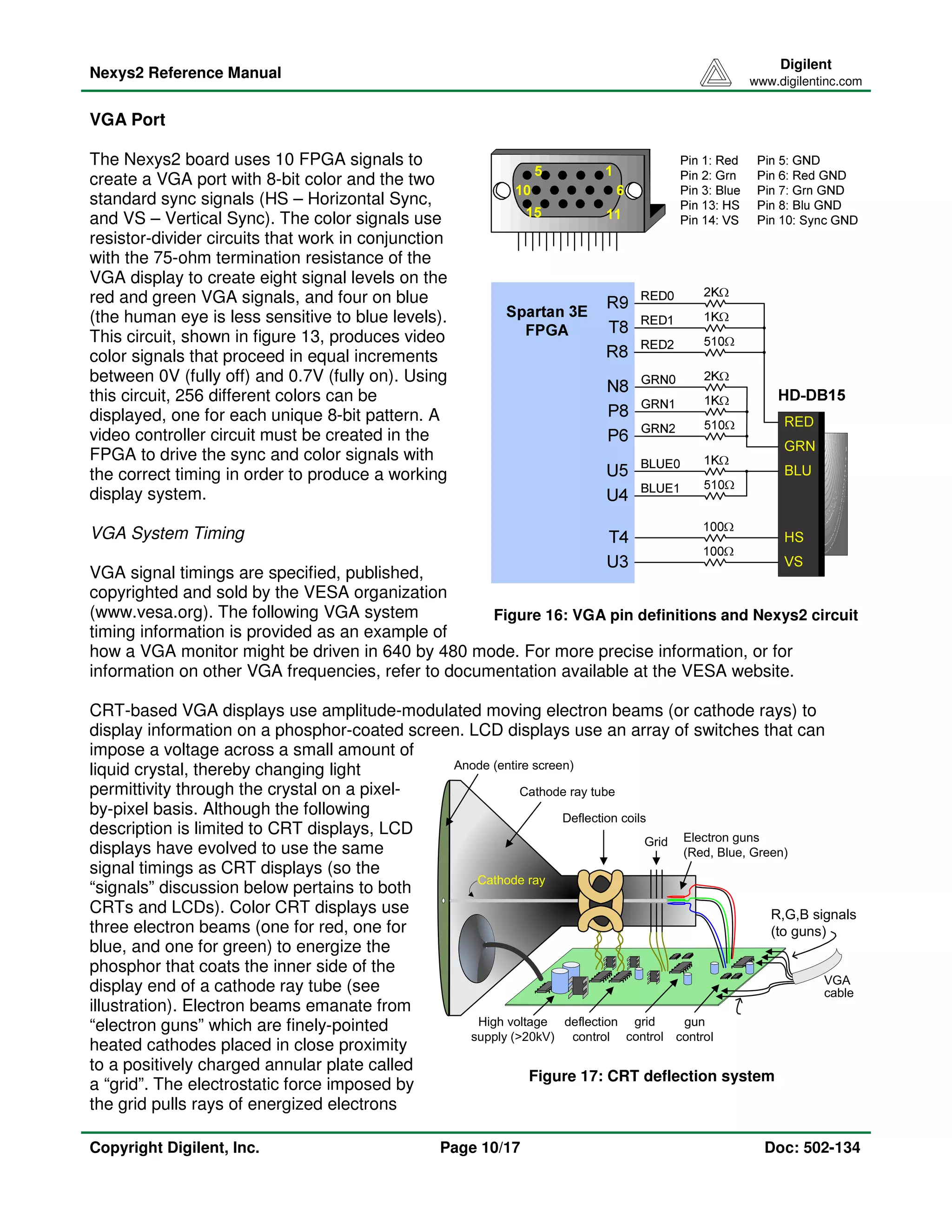
Download to read offline
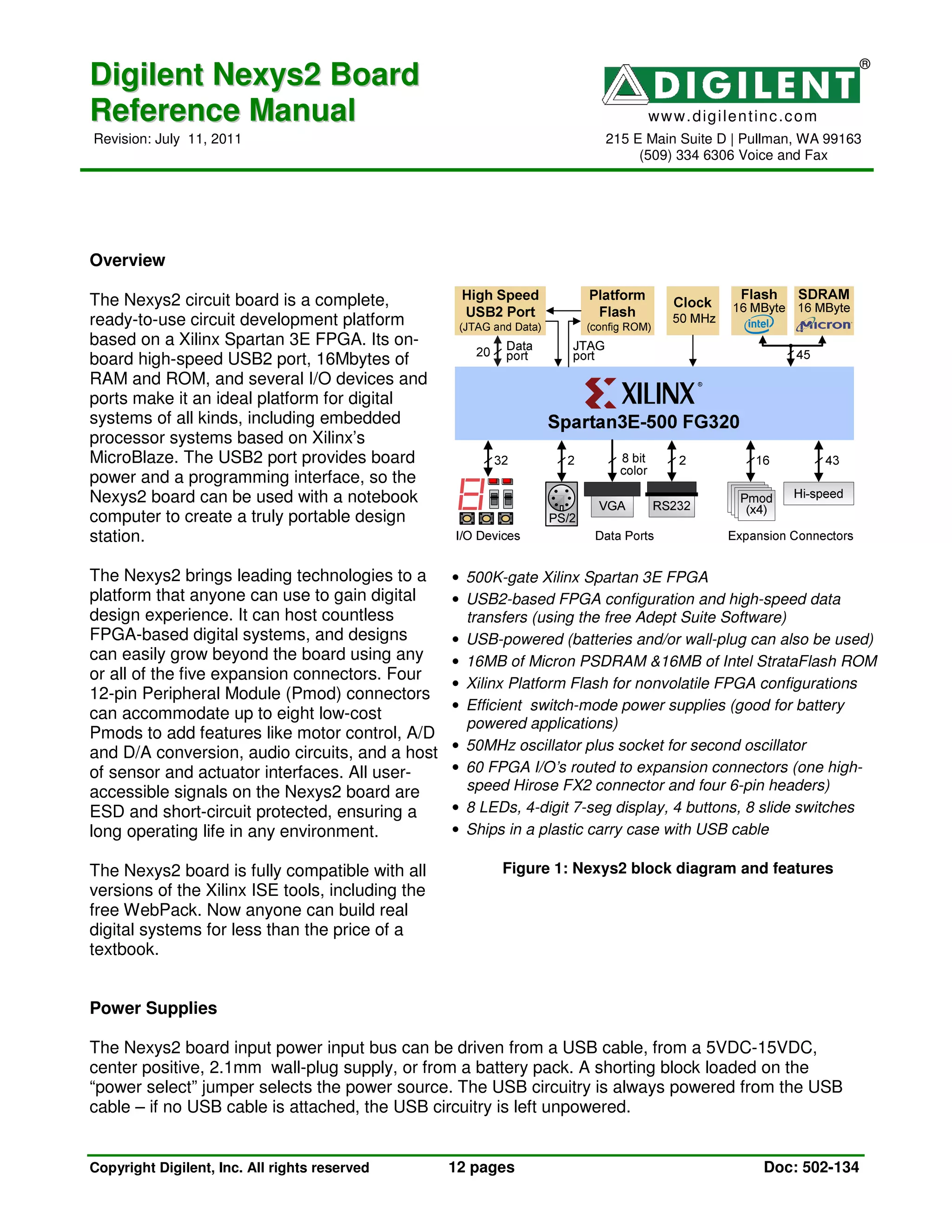
Diigiillentt Nexys2 Board 
Refference Manuall 
® 
www.digi lent inc.com 
Revision: July 11, 2011 215 E Main Suite D | Pullman, WA 99163 
(509) 334 6306 Voice and Fax 
Overview 
The Nexys2 circuit board is a complete, 
ready-to-use circuit development platform 
based on a Xilinx Spartan 3E FPGA. Its on-board 
high-speed USB2 port, 16Mbytes of 
RAM and ROM, and several I/O devices and 
ports make it an ideal platform for digital 
systems of all kinds, including embedded 
processor systems based on Xilinx’s 
MicroBlaze. The USB2 port provides board 
power and a programming interface, so the 
Nexys2 board can be used with a notebook 
computer to create a truly portable design 
station. 
The Nexys2 brings leading technologies to a 
platform that anyone can use to gain digital 
design experience. It can host countless 
FPGA-based digital systems, and designs 
can easily grow beyond the board using any 
or all of the five expansion connectors. Four 
12-pin Peripheral Module (Pmod) connectors 
can accommodate up to eight low-cost 
Pmods to add features like motor control, A/D 
and D/A conversion, audio circuits, and a host 
of sensor and actuator interfaces. All user-accessible 
signals on the Nexys2 board are 
ESD and short-circuit protected, ensuring a 
long operating life in any environment. 
The Nexys2 board is fully compatible with all 
versions of the Xilinx ISE tools, including the 
free WebPack. Now anyone can build real 
digital systems for less than the price of a 
textbook. 
Power Supplies 
• 500K-gate Xilinx Spartan 3E FPGA 
• USB2-based FPGA configuration and high-speed data 
transfers (using the free Adept Suite Software) 
• USB-powered (batteries and/or wall-plug can also be used) 
• 16MB of Micron PSDRAM &16MB of Intel StrataFlash ROM 
• Xilinx Platform Flash for nonvolatile FPGA configurations 
• Efficient switch-mode power supplies (good for battery 
powered applications) 
• 50MHz oscillator plus socket for second oscillator 
• 60 FPGA I/O’s routed to expansion connectors (one high-speed 
Hirose FX2 connector and four 6-pin headers) 
• 8 LEDs, 4-digit 7-seg display, 4 buttons, 8 slide switches 
• Ships in a plastic carry case with USB cable 
Figure 1: Nexys2 block diagram and features 
The Nexys2 board input power input bus can be driven from a USB cable, from a 5VDC-15VDC, 
center positive, 2.1mm wall-plug supply, or from a battery pack. A shorting block loaded on the 
“power select” jumper selects the power source. The USB circuitry is always powered from the USB 
cable – if no USB cable is attached, the USB circuitry is left unpowered. 
Copyright Digilent, Inc. All rights reserved 12 pages Doc: 502-134
Nexys2 Reference Manual 
Digilent 
www.digilentinc.com 
Figure 2: Nexys2 power supply block diagram 
Table 1: Nexys2 Power Supplies 
Supply Device Amps (max/typ) 
3.3V main IC6: LTC1765 3A/100mA 
2.5V FPGA IC7: LTC3417 1.4A/50mA 
1.2V FPGA IC7: LTC3417 1.4A/200mA 
1.8V SRAM IC8: LTC1844 150mA/90mA 
3.3V USB IC5: LTC1844 150mA/60mA 
Figure 3: Nexys2 power supply jumpers 
The input power bus drives a 3.3V voltage regulator 
that supplies all required board current. Some devices 
require 2.5V, 1.8V, and 1.2V supplies in addition to the 
main 3.3V supply, and these additional supplies are 
created by regulators that take their input from the 
main 3.3V supply. The primary supplies are generated 
by highly efficient switching regulators from Linear 
Technology. These regulators not only use USB power 
efficiently, they also allow the Nexys2 to run from 
battery packs for extended periods. 
Total board current depends on the FPGA configuration, 
clock frequency, and external connections. In test 
circuits with roughly 20K gates routed, a 50MHz clock 
source, and all LEDs illuminated, about 200mA of 
current is drawn from the 1.2V supply, 50mA from the 
2.5V supply, and 100mA from the 3.3V supply. Required 
current will increase if larger circuits are configured in 
the FPGA, and if peripheral boards are attached. The 
table above summarizes the power supply parameters. 
The Nexys2 board can also receive power from (or 
deliver power to) a peripheral board connected to a 
Pmod connector or to the large 100-pin expansion 
connector. Jumpers near the Pmod connectors and 
large expansion connector (JP1 – JP5) can connect the 
Nexys2’s input power bus to the connector’s power pins. 
The Pmod jumpers can be used to route either the input 
power bus or regulated 3.3V to the Pmod power pins, 
while the expansion connector jumper can only make or 
break a connection with the input power bus. 
USB power is supplied to the USB circuitry directly, but 
to the rest of the board through an electronic switch (Q1 
in the Nexys2 schematic). The on-board USB controller 
turns on switch Q1 only after informing the host PC that 
Copyright Digilent, Inc. Page 2/17 Doc: 502-134
Nexys2 Reference Manual 
Digilent 
www.digilentinc.com 
more than 100mA will be drawn through the USB cable (as required by the USB specification). A USB 
host can supply only 500mA of current at 5VDC. When using USB power, care must be taken to 
ensure the Nexys2 board and any attached peripheral boards do not draw more than 500mA, or 
damage to the host may result. The Nexys2 board typically consumes about 300mA of USB current, 
leaving about 200mA for peripheral boards. If peripheral boards require more current than the USB 
cable can supply, an external power supply should be used. 
The Nexys2 board uses a six layer PCB, with the inner layers dedicated to VCC and GND planes. 
The FPGA and the other ICs on the board all have a large complement of bypass capacitors placed 
as close as possible to each VCC pin. The power supply routing and bypass capacitors result in a 
very clean, stable, and low-noise power supply. 
FPGA and Platform Flash Configuration 
The FPGA on the Nexys2 board must be configured (or programmed) by the user before it can 
perform any functions. During configuration, a “bit” file is transferred into memory cells within the 
FPGA to define the logical functions and circuit interconnects. The free ISE/WebPack CAD software 
from Xilinx can be used to create bit files from VHDL, Verilog, or schematic-based source files. 
The FPGA can be programmed in two ways: 
directly from a PC using the on-board USB port, 
and from an on-board Platform Flash ROM (the 
Flash ROM is also user-programmable via the 
USB port). A jumper on the Nexys2 board 
determines which source (PC or ROM) the 
FPGA will use to load its configuration. The 
FPGA will automatically load a configuration 
from the Platform Flash ROM at power-on if the 
configuration Mode jumper is set to “Master 
serial”. If the Mode jumper is set to “JTAG”, the 
FPGA will await programming from the PC (via 
the USB cable). 
Cypress 
EZ-USB 
USB miniB 
connector 
XCF02 
Platform 
Flash 
JTAG 
header 
JTAG 
Mode 
Jumper 
Spartan 3E 
FPGA 
PROG 
DONE 
Vdd 
Done 
LED 
JTAG 
port 
Slave 
serial 
port 
Digilent’s freely available PC-based Adept 
software can be used to configure the FPGA 
and Platform Flash with any suitable file stored 
on the computer. Adept uses the USB cable to 
transfer a selected bit file from the PC to the FPGA or Platform Flash ROM. After the FPGA is 
configured, it will remain so until it is reset by a power-cycle event or by the FPGA reset button 
(BTNR) being pressed. The Platform Flash ROM will retain a bit file until it is reprogrammed, 
regardless of power-cycle events. 
FPGA 
Reset 
Button 
(BTNR) 
Figure 4: Nexys2 programming circuits 
To program the Nexys2 board using Adept, attach the USB cable to the board (if USB power will not 
be used, attach a suitable power supply to the power jack or battery connector on the board, and set 
the power switch to “wall” or “bat”). Start the Adept software, and wait for the FPGA and the Platform 
Flash ROM to be recognized. Use the browse function to associate the desired .bit file with the FPGA, 
and/or the desired .mcs file with the Platform Flash ROM. Right-click on the device to be 
programmed, and select the “program” function. The configuration file will be sent to the FPGA or 
Platform Flash, and the software will indicate whether programming was successful. The configuration 
Copyright Digilent, Inc. Page 3/17 Doc: 502-134
Nexys2 Reference Manual 
Digilent 
www.digilentinc.com 
Figure 5: Nexys2 board programming circuits 
“done” LED will illuminate after the FPGA has been 
successfully configured. For further information on 
using Adept, please see the Adept documentation 
available at the Digilent website. 
The Nexys2 board can also be programmed using 
Xilinx’s iMPACT software by connecting a suitable 
programming cable to the JTAG header. Digilent’s 
JTAG3 cable or any other Xilinx cable may be 
used. 
A demonstration configuration is loaded into the 
Platform Flash on the Nexys2 board during 
manufacturing. That configuration, also available 
on the Digilent webpage, can be used to check all 
of the devices and circuits on the Nexys2 board. 
The Nexys2 board includes a 50MHz oscillator and a socket for a 
second oscillator. Clock signals from the oscillators connect to 
global clock input pins on the FPGA so they can drive the clock 
synthesizer blocks available in FPGA. The clock synthesizers 
(called DLLs, or delay locked loops) provide clock management 
capabilities that include doubling or quadrupling the input 
frequency, dividing the input frequency by any integer multiple, 
and defining precise phase and delay relationships between 
various clock signals. 
Figure 6: Nexys2 clocks 
The Nexys2 board includes several input devices, output devices, and data ports, allowing many 
designs to be implemented without the need for any other components. 
Figure 7: Nexys2 board I/O devices 
Clocks 
User I/O 
Inputs: Slide Switches and Pushbuttons 
Four pushbuttons and eight slide switches are provided for circuit inputs. Pushbutton inputs are 
normally low, and they are driven high only when the pushbutton is pressed. Slide switches generate 
constant high or low inputs depending on their position. Pushbutton and slide switch inputs use a 
Copyright Digilent, Inc. Page 4/17 Doc: 502-134
Nexys2 Reference Manual 
Digilent 
www.digilentinc.com 
series resistor for protection against short circuits (a short circuit would occur if an FPGA pin assigned 
to a pushbutton or slide switch was inadvertently defined as an output). 
Figure 8: Nexys2 I/O devices and circuits 
Outputs: LEDs 
Eight LEDs are provided for circuit outputs. LED anodes are driven from the FPGA via 390-ohm 
resistors, so a logic ‘1’ output will illuminate them with 3-4ma of drive current. A ninth LED is provided 
as a power-on LED, and a tenth LED indicates FPGA programming status. Note that LEDs 4-7 have 
different pin assignments due to pinout differences between the -500 and the -1200 die. 
Outputs: Seven-Segment Display 
The Nexys2 board contains a four-digit common anode seven-segment LED display. Each of the four 
digits is composed of seven segments arranged in a “figure 8” pattern, with an LED embedded in 
each segment. Segment LEDs can be individually illuminated, so any one of 128 patterns can be 
displayed on a digit by illuminating certain LED segments and leaving the others dark. Of these 128 
possible patterns, the ten corresponding to the decimal digits are the most useful. 
Copyright Digilent, Inc. Page 5/17 Doc: 502-134
Nexys2 Reference Manual 
Digilent 
www.digilentinc.com 
The anodes of the seven LEDs forming each digit are tied together into one “common anode” circuit 
node, but the LED cathodes remain separate. The common anode signals are available as four “digit 
enable” input signals to the 4-digit display. The cathodes of similar segments on all four displays are 
connected into seven circuit nodes labeled CA through CG (so, for example, the four “D” cathodes 
from the four digits are grouped together into a single circuit node called “CD”). These seven cathode 
signals are available as inputs to the 4-digit display. This signal connection scheme creates a 
multiplexed display, where the cathode signals are common to all digits but they can only illuminate 
the segments of the digit whose corresponding anode signal is asserted. 
An un-illuminated seven-segment display, and nine 
illumination patterns corresponding to decimal digits 
Figure 9: Nexys2 seven-segment displays 
A scanning display controller circuit can be used to show a four-digit number on this display. This 
circuit drives the anode signals and corresponding cathode patterns of each digit in a repeating, 
continuous succession, at an update rate that is faster than the human eye can detect. Each digit is 
illuminated just one-quarter of the time, but because the eye cannot perceive the darkening of a digit 
before it is illuminated again, the digit appears continuously illuminated. If the update or “refresh” rate 
is slowed to around 45 hertz, most people will begin to see the display flicker. 
In order for each of the four digits to appear bright and continuously illuminated, all four digits should 
be driven once every 1 to 16ms, for a refresh frequency of 1KHz to 60Hz. For example, in a 60Hz 
refresh scheme, the entire display would be refreshed once every 16ms, and each digit would be 
illuminated for ¼ of the refresh cycle, or 4ms. The controller must drive the cathodes with the correct 
pattern when the corresponding 
anode signal is driven. To illustrate 
Refresh period = 1ms to 16ms 
the process, if AN0 is asserted while 
CB and CC are asserted, then a “1” 
Digit period = Refresh / 4 
will be displayed in digit position 1. 
AN1 
Then, if AN1 is asserted while CA, CB 
and CC are asserted, then a “7” will 
AN2 
be displayed in digit position 2. If AN0 
AN3 
and CB, CC are driven for 4ms, and 
then A1 and CA, CB, CC are driven 
AN4 
for 4ms in an endless succession, the 
Cathodes Digit 0 
Digit 1 Digit 2 Digit 3 
display will show “17” in the first two 
digits. An example timing diagram for 
Figure 10: Seven-segment display timing diagram 
a four-digit controller is provided. 
Copyright Digilent, Inc. Page 6/17 Doc: 502-134
Nexys2 Reference Manual 
Digilent 
www.digilentinc.com 
USB Port 
The Nexys2 includes a high-speed USB2 
port based on a Cypress CY7C68013A USB 
controller. The USB port can be used to 
program the on-board Xilinx devices, to 
perform user-data transfers at up to 
38Mbytes/sec, and to provide power to the 
board. Programming is accomplished with 
Digilent’s free Adept Suite Software. User 
data transfers can also be accomplished 
using the Adept software, or custom user 
software can be written using Digilent’s 
public API’s to access the Nexys2 USB 
connection. Information on using Adept 
and/or the public API’s to transfer data can 
be found on the Digilent website. 
Figure 11: Nexys2 USB circuit 
The USB port can also provide power to the Nexys2 board if the power select jumper is set to “USB”. 
The USB specification requires that attached devices draw no more than 100mA until they have 
requested more current, after which up to 500mA may be drawn. When first attached to a USB host, 
the Nexys2 board requests 500mA, and then activates a transistor switch to connect the USB cable 
voltage to the main input power bus. The Nexys2 board typically draws around 300mA from the USB 
cable, and care should be taken (especially when using peripheral boards) to ensure that no more 
than 500mA is drawn. 
PS/2 Port 
The 6-pin mini-DIN connector can accommodate a PS/2 mouse or keyboard. Most PS/2 devices can 
operate from a 3.3V supply, but older devices may require a 5VDC supply. A three-pin jumper on the 
Nexys2 board immediately adjacent to the PS/2 connector selects whether regulated 3.3V or the main 
input power bus voltage (VU) is supplied to the PS/2 connector. To send 5V to the PS/2 connector, 
set the PS2 power jumper to Vswt (the main input power bus), and ensure the board is powered from 
USB or a 5VDC wall-plug supply. To send 3.3V to the connector, set the jumper to 3.3V. 
Figure 12: Nexys2 PS/2 circuits 
Both the mouse and keyboard use a two-wire serial bus (clock and data) to communicate with a host 
device. Both use 11-bit words that include a start, stop and odd parity bit, but the data packets are 
organized differently, and the keyboard interface allows bi-directional data transfers (so the host 
Copyright Digilent, Inc. Page 7/17 Doc: 502-134
Nexys2 Reference Manual 
Digilent 
www.digilentinc.com 
device can illuminate state LEDs on the keyboard). 
Bus timings are shown in the figure. The clock and 
data signals are only driven when data transfers 
occur, and otherwise they are held in the “idle” 
state at logic ‘1’. The timings define signal 
requirements for mouse-to-host communications 
and bi-directional keyboard communications. A 
PS/2 interface circuit can be implemented in the 
FPGA to create a keyboard or mouse interface. 
Keyboard 
Figure 13: PS/2 signal timings 
The keyboard uses open-collector drivers so the keyboard or an attached host device can drive the 
two-wire bus (if the host device will not send data to the keyboard, then the host can use input-only 
ports). 
PS2-style keyboards use scan codes to communicate key press data. Each key is assigned a code 
that is sent whenever the key is pressed; if the key is held down, the scan code will be sent repeatedly 
about once every 100ms. When a key is released, a “F0” key-up code is sent, followed by the scan 
code of the released key. If a key can be “shifted” to produce a new character (like a capital letter), 
then a shift character is sent in addition to the scan code, and the host must determine which ASCII 
character to use. Some keys, called extended keys, send an “E0” ahead of the scan code (and they 
may send more than one scan code). When an extended key is released, an “E0 F0” key-up code is 
sent, followed by the scan code. Scan codes for most keys are shown in the figure. A host device can 
also send data to the keyboard. Below is a short list of some common commands a host might send. 
ED Set Num Lock, Caps Lock, and Scroll Lock LEDs. Keyboard returns “FA” after receiving “ED”, 
then host sends a byte to set LED status: Bit 0 sets Scroll Lock; bit 1 sets Num Lock; and Bit 2 
sets Caps lock. Bits 3 to 7 are ignored. 
EE Echo (test). Keyboard returns “EE” after receiving “EE”. 
F3 Set scan code repeat rate. Keyboard returns “F3” on receiving “FA”, then host sends second 
byte to set the repeat rate. 
FE Resend. “FE” directs keyboard to re-send most recent scan code. 
FF Reset. Resets the keyboard. 
The keyboard can send data to the host only when both the data and clock lines are high (or idle). 
Since the host is the “bus master”, the keyboard must check to see whether the host is sending data 
before driving the bus. To facilitate this, the clock line is used as a “clear to send” signal. If the host 
pulls the clock line low, the keyboard must not send any data until the clock is released. The keyboard 
sends data to the host in 11-bit words that contain a ‘0’ start bit, followed by 8-bits of scan code (LSB 
first), followed by an odd parity bit and terminated with a ‘1’ stop bit. The keyboard generates 11 clock 
transitions (at around 20 - 30KHz) when the data is sent, and data is valid on the falling edge of the 
clock. 
Scan codes for most PS/2 keys are shown in the figure below. 
Copyright Digilent, Inc. Page 8/17 Doc: 502-134
Nexys2 Reference Manual 
Digilent 
www.digilentinc.com 
Mouse 
Figure 14: PS/2 keyboard scan codes 
The mouse outputs a clock and data signal when it is moved; otherwise, these signals remain at logic 
‘1’. Each time the mouse is moved, three 11-bit words are sent from the mouse to the host device. 
Each of the 11-bit words contains a ‘0’ start bit, followed by 8 bits of data (LSB first), followed by an 
odd parity bit, and terminated with a ‘1’ stop bit. Thus, each data transmission contains 33 bits, where 
bits 0, 11, and 22 are ‘0’ start bits, and bits 10, 21, and 33 are ‘1’ stop bits. The three 8-bit data fields 
contain movement data as shown in the figure above. Data is valid at the falling edge of the clock, and 
the clock period is 20 to 30KHz. 
The mouse assumes a relative coordinate system wherein moving the mouse to the right generates a 
positive number in the X field, and moving to the left generates a negative number. Likewise, moving 
the mouse up generates a positive number in the Y field, and moving down represents a negative 
number (the XS and YS bits in the status byte are the sign bits – a ‘1’ indicates a negative number). 
The magnitude of the X and Y numbers represent the rate of mouse movement – the larger the 
number, the faster the mouse is moving (the XV and YV bits in the status byte are movement overflow 
indicators – a ‘1’ means overflow has occurred). If the mouse moves continuously, the 33-bit 
transmissions are repeated every 50ms or so. The L and R fields in the status byte indicate Left and 
Right button presses (a ‘1’ indicates the button is being pressed). 
Figure 15: Mouse data format 
Copyright Digilent, Inc. Page 9/17 Doc: 502-134
Nexys2 Reference Manual 
Digilent 
www.digilentinc.com 
VGA Port 
The Nexys2 board uses 10 FPGA signals to 
create a VGA port with 8-bit color and the two 
standard sync signals (HS – Horizontal Sync, 
and VS – Vertical Sync). The color signals use 
resistor-divider circuits that work in conjunction 
with the 75-ohm termination resistance of the 
VGA display to create eight signal levels on the 
red and green VGA signals, and four on blue 
(the human eye is less sensitive to blue levels). 
This circuit, shown in figure 13, produces video 
color signals that proceed in equal increments 
between 0V (fully off) and 0.7V (fully on). Using 
this circuit, 256 different colors can be 
displayed, one for each unique 8-bit pattern. A 
video controller circuit must be created in the 
FPGA to drive the sync and color signals with 
the correct timing in order to produce a working 
display system. 
VGA System Timing 
VGA signal timings are specified, published, 
copyrighted and sold by the VESA organization 
(www.vesa.org). The following VGA system 
timing information is provided as an example of 
how a VGA monitor might be driven in 640 by 480 mode. For more precise information, or for 
information on other VGA frequencies, refer to documentation available at the VESA website. 
Figure 16: VGA pin definitions and Nexys2 circuit 
CRT-based VGA displays use amplitude-modulated moving electron beams (or cathode rays) to 
display information on a phosphor-coated screen. LCD displays use an array of switches that can 
impose a voltage across a small amount of 
liquid crystal, thereby changing light 
permittivity through the crystal on a pixel-by- 
pixel basis. Although the following 
description is limited to CRT displays, LCD 
displays have evolved to use the same 
signal timings as CRT displays (so the 
“signals” discussion below pertains to both 
CRTs and LCDs). Color CRT displays use 
three electron beams (one for red, one for 
blue, and one for green) to energize the 
phosphor that coats the inner side of the 
display end of a cathode ray tube (see 
illustration). Electron beams emanate from 
“electron guns” which are finely-pointed 
heated cathodes placed in close proximity 
to a positively charged annular plate called 
a “grid”. The electrostatic force imposed by 
the grid pulls rays of energized electrons 
Anode (entire screen) 
Cathode ray tube 
Cathode ray 
High voltage 
supply (>20kV) 
Deflection coils 
Grid Electron guns 
(Red, Blue, Green) 
gun 
control 
grid 
control 
deflection 
control 
R,G,B signals 
(to guns) 
VGA 
cable 
Figure 17: CRT deflection system 
Copyright Digilent, Inc. Page 10/17 Doc: 502-134
Nexys2 Reference Manual 
Digilent 
www.digilentinc.com 
from the cathodes, and those rays are fed by the current that flows into the cathodes. These particle 
rays are initially accelerated towards the grid, but they soon fall under the influence of the much larger 
electrostatic force that results from the entire phosphor-coated display surface of the CRT being 
charged to 20kV (or more). The rays are focused to a fine beam as they pass through the center of 
the grids, and then they accelerate to impact on the phosphor-coated display surface. The phosphor 
surface glows brightly at the impact point, and it continues to glow for several hundred microseconds 
after the beam is removed. The larger the current fed into the cathode, the brighter the phosphor will 
glow. 
Between the grid and the display surface, the beam passes through the neck of the CRT where two 
coils of wire produce orthogonal electromagnetic fields. Because cathode rays are composed of 
charged particles (electrons), they can be deflected by these magnetic fields. Current waveforms are 
passed through the coils to produce magnetic fields that interact with the cathode rays and cause 
them to transverse the display surface in a “raster” pattern, horizontally from left to right and vertically 
from top to bottom. As the cathode ray moves over the surface of the display, the current sent to the 
electron guns can be increased or decreased to change the brightness of the display at the cathode 
ray impact point. 
Information is only displayed when the beam is moving in the “forward” direction (left to right and top 
to bottom), and not during the time the beam is reset back to the left or top edge of the display. Much 
of the potential display time is therefore lost in “blanking” periods when the beam is reset and 
stabilized to begin a new horizontal or vertical display pass. The size of the beams, the frequency at 
which the beam can be traced across the display, and the frequency at which the electron beam can 
be modulated determine the display 
resolution. Modern VGA displays can 
accommodate different resolutions, 
and a VGA controller circuit dictates 
the resolution by producing timing 
signals to control the raster patterns. 
The controller must produce 
synchronizing pulses at 3.3V (or 5V) to 
set the frequency at which current 
flows through the deflection coils, and 
it must ensure that video data is 
applied to the electron guns at the 
correct time. Raster video displays 
define a number of “rows” that 
corresponds to the number of 
horizontal passes the cathode makes 
over the display area, and a number of 
“columns” that corresponds to an area 
on each row that is assigned to one 
“picture element” or pixel. Typical 
displays use from 240 to 1200 rows 
and from 320 to 1600 columns. The 
overall size of a display and the 
number of rows and columns 
determines the size of each pixel. 
Video data typically comes from a 
video refresh memory, with one or 
Current 
waveform 
through 
horizontal 
defletion 
coil 
pixel 0,0 pixel 0,639 
640 pixels per row are displayed 
during forward beam trace 
Display Surface 
pixel 479,0 pixel 479,639 
Stable current ramp - information 
is displayed during this time 
Retrace - no 
information 
displayed 
during this 
time 
Total horizontal time 
Horizontal display time 
HS time 
Horizontal sync signal 
sets retrace frequency 
retrace 
time 
"front porch" "back porch" 
Figure 18: VGA system signals 
Copyright Digilent, Inc. Page 11/17 Doc: 502-134
Nexys2 Reference Manual 
Digilent 
www.digilentinc.com 
more bytes assigned to each pixel location (the Nexys2 uses three bits per pixel). The controller must 
index into video memory as the beams move across the display, and retrieve and apply video data to 
the display at precisely the time the electron beam is moving across a given pixel. 
A VGA controller circuit must generate the 
TS 
HS and VS timings signals and coordinate 
Tthe delivery of video data based on the pixel 
fp 
Tdisp 
clock. The pixel clock defines the time 
available to display one pixel of information. 
TThe VS signal defines the “refresh” 
pw 
Tbp 
frequency of the display, or the frequency at 
which all information on the display is 
Vertical Sync 
Horiz. Sync 
Symbol Parameter 
redrawn. The minimum refresh frequency is 
Time Clocks Lines 
Time 
Clks 
a function of the display’s phosphor and 
T 
S 
Sync pulse 
16.7ms 
416,800 
521 
32 us 
800 
electron beam intensity, with practical 
T 
disp 
Display time 
15.36ms 
384,000 
480 
25.6 us 
640 
refresh frequencies falling in the 50Hz to 
T 
pw 
Pulse width 
64 us 
1,600 
2 
3.84 us 
96 
120Hz range. The number of lines to be 
T 
Front porch 
320 us 
8,000 
10 
640 ns 
16 
displayed at a given refresh frequency 
fp 
T 
defines the horizontal “retrace” frequency. 
bp 
Back porch 
928 us 
23,200 
29 
1.92 us 
48 
For a 640-pixel by 480-row display using a 
25MHz pixel clock and 60 +/-1Hz refresh, 
Figure 19: VGA system timings for 640x480 display 
the signal timings shown in the table at right 
can be derived. Timings for sync pulse width and front and back porch intervals (porch intervals are 
the pre- and post-sync pulse times during which information cannot be displayed) are based on 
observations taken from actual VGA displays. 
A VGA controller circuit decodes the output of a horizontal-sync counter driven by the pixel clock to 
generate HS signal timings. This counter can be used to locate any pixel location on a given row. 
Likewise, the output of a vertical-sync counter that increments with each HS pulse can be used to 
generate VS signal timings, and this counter can be used to locate any given row. These two 
continually running counters can be used to form an address into video RAM. No time relationship 
between the onset of the HS pulse and the onset of the VS pulse is specified, so the designer can 
arrange the counters to easily form video RAM addresses, or to minimize decoding logic for sync 
pulse generation. 
Figure 20: Schematic for a VGA controller circuit 
Copyright Digilent, Inc. Page 12/17 Doc: 502-134
Nexys2 Reference Manual 
Digilent 
www.digilentinc.com 
Serial Port 
The Nexys2 contains a two-wire serial port based on an ST Microelectronics ST3232 voltage 
converter. The ST3232 converts the signal levels used by RS-232 communications (-12 to -3 for a 
logic ‘1’ and 12V to 3V for a logic ‘0’) to the 3.3V signals used by the FPGA. Since only two signals 
are connected (RXD and TXD), an FPGA-based serial port controller can only use software hand-shaking 
protocols (XON/XOFF). The Nexys2 serial port is useful for many applications, and in 
particular for debugging and working with Xilinx’s MicroBlaze embedded processor. 
The two devices connected to either end of a serial cable are known as the Data Terminal Equipment 
(DTE) and the Data Communications Equipment (DCE). The DCE was originally conceived to be a 
modem, but now many devices connect to a computer as a DCE. A DTE “source” device uses a male 
DB-9 connector, and a DCE 
“peripheral” device uses a female 
DB-9 connector. Two DTE devices 
can be connected via a serial 
cable only if lines two and three 
(RXD and TXD) are crossed, 
producing what is known as a null 
modem cable. A DTE and DCE 
device can be connected with a 
straight-through cable. The 
Nexys2 is configured as a DCE 
device, with the assumption it will 
most typically be connected to a 
DTE device like a computer. 
Memory 
P9 
U6 100 
Spartan 3E 
FPGA 
DB-9 
DCD 
RXD 
TXD 
DTR 
SG 
DSR 
RTS 
CTS 
RI 
1 
2 
3 
4 
5 
6 
7 
8 
9 
T1OUT 
R1IN 
T1IN 
R1OUT 
ST3232 
RS-232 
voltage 
converter 
Figure 21: Nexys2 serial port circuit 
The Nexys2 board has external RAM and ROM devices. The external RAM is a 128Mbit Micron 
M45W8MW16 Cellular RAM pseudo-static DRAM device organized as 8Mbytes x 16bits. It can 
operate as a typical asynchronous SRAM with read and write cycle times of 70ns, or as a 
synchronous memory with an 80MHz bus. When operated as an asynchronous SRAM, the Cellular 
RAM automatically refreshes its internal DRAM arrays, allowing for a simplified memory controller 
design (similar to any SRAM) in the FPGA. When operated in synchronous mode, continuous 
transfers of up to 80MHz are possible. 
The external ROM is a 128Mbit Intel TE28F128J3D75-110 StrataFlash device organized as 8Mbytes 
x 16bits. Internally, it contains 128 blocks that can be individually erased, and it supports 110ns read 
cycle times, with 25ns page-mode reads within blocks. It has an internal 32-byte write buffer that can 
be written with 70ns cycle times, and the 32-byte buffer can be transferred to the Flash array in 218us 
(typical). 
Both devices share a common 16-bit data bus and 24-bit address bus. The Cellular RAM is byte 
addressable using the upper-byte and lower-byte signals (MT-UB and MT-LB), but the StrataFlash is 
configured for 16 byte operations only (it is not byte addressable). The output enable (OE) and write 
enable (WE) signals are shared by both devices, but each device has individual chip enable (CE) 
signals. Additionally, the Cellular RAM has clock (MT-CLK), wait (MT-WAIT), address valid (MT-ADV) 
and control register enable (MT_CRE) signals available to the FPGA for use with synchronous 
transfers, and the StrataFlash has Reset (RP#) and status (STS) signals routed to the FPGA. 
Copyright Digilent, Inc. Page 13/17 Doc: 502-134
Nexys2 Reference Manual 
Digilent 
www.digilentinc.com 
VDHL source code is available in a reference design posted on the Digilent website to illustrate the 
use of these devices. A base system builder file is also available for using these devices with Xilinx’s 
EDK tool and MicroBlaze processor core, both available from Xilinx. Complete information is available 
for both devices from the manufacturer websites. 
Figure 22: Nexys2 memory circuits 
Table 2: Memory Address and Data Bus Pin Assignments 
Address signals Data signals 
ADDR0: NA ADDR8: H6 ADDR16: M5 DATA0: L1 DATA8: L3 
ADDR1: J1 ADDR9: F1 ADDR17: E2 DATA1: L4 DATA9: L5 
ADDR2: J2 ADDR10: G3 ADDR18: C2 DATA2: L6 DATA10: M3 
ADDR3: H4 ADDR11: G6 ADDR19: C1 DATA3: M4 DATA11: M6 
ADDR4: H1 ADDR12: G5 ADDR20: D2 DATA4: N5 DATA12: L2 
ADDR5: H2 ADDR13: G4 ADDR21: K3 DATA5: P1 DATA13: N4 
ADDR6: J5 ADDR14: F2 ADDR22: D1 DATA6: P2 DATA14: R3 
ADDR7: H3 ADDR15: E1 ADDR23: K6 DATA7: R2 DATA15: T1 
Copyright Digilent, Inc. Page 14/17 Doc: 502-134
Nexys2 Reference Manual 
Digilent 
www.digilentinc.com 
Peripheral Connectors 
The Nexys2 board provides four two-row 6-pin Pmod connectors that together can accommodate up 
to 8 Pmods. The four 12-pin connectors each have 8 data signals, two GND pins, and two Vdd pins. 
All data signals include short circuit protection resistors and ESD protection Diodes. A jumper block 
adjacent to each Pmod connector can connect the Pmod’s Vdd signal to the Nexys2 board’s 3.3V 
supply or to the input power bus (VU). If the jumper is set to VU and USB power is driving the main 
power bus, care should be taken to ensure no more than 200mA is consumed by the Pmod. Further, if 
the jumper is set to VU, a voltage source connected to the Pmod can drive the main power bus of the 
Nexys2 board, so care should be taken to avoid connecting conflicting power supplies. 
The Pmod connectors are labeled JA (nearest the power jack), JB, JC, and JD (nearest the expansion 
connector). Pinouts for the Pmod connectors are provided in the table below. 
More than 30 low-cost are available for attachment to these connectors. Pmods can either be 
attached directly, or by using a small cable. Available Pmods include A/D and D/A converters, motor 
drivers, speaker amplifiers, distance measuring devices, etc. Please see www.digilentinc.com for 
more information. 
7 
1 
8 
9 
4 
10 
5 
11 
6 
5 
12 
JA 
JA1 
JA2 
JA3 
JA4 
JA5 
JA6 
JA7 
JA8 
Spartan 3E 
FPGA 
Resistors for short-circuit 
ESD protection 
diodes 
1 
protection 
2 
3 
Power supply 
jumper 
Figure 23: Nexys2 Pmod connector circuits 
Table 3: Nexys2 Pmod Connector Pin Assignments 
VU 
3.3V 
Pmod JA Pmod JB Pmod JC Pmod JD 
JA1: L15 JA7: K13 JB1: M13 JB7: P17 JC1: G15 JC7: H15 JD1: J13 JD7: K141 
JA2: K12 JA8: L16 JB2: R18 JB8: R16 JC2: J16 JC8: F14 JD2: M18 JD8: K152 
JA3: L17 JA9: M14 JB3: R15 JB9: T18 JC3: G13 JC9: G16 JD3: N18 JD9: J153 
JA4: M15 JA10: M16 JB4: T17 JB10: U18 JC4: H16 JC10: J12 JD4:; P18 JD10: J144 
Notes: 1 shared with LD3 2 shared with LD3 3 shared with LD3 4 shared with LD3 
Copyright Digilent, Inc. Page 15/17 Doc: 502-134
Nexys2 Reference Manual 
Digilent 
www.digilentinc.com 
Expansion connector 
The Nexys2 board includes a Hirose FX-2 high-density 
100 pin connector that is suitable for 
driving peripheral boards with signal rates in 
excess of 100 MHz. Many connector signals are 
routed to the FPGA as differential pairs, and 47 
connector pins are tied to ground, resulting in a 
very low-noise connection system. The self-aligning 
Hirose FX-2 connector can be used for 
board-to-board connections or board-to-cable 
connections using the mating Hirose FX2-100S- 
1.27 available from many catalog distributors 
and directly from Digilent. 
All signals routed from the FPGA to the FX-2 
connector include 75-ohm series resistors. The 
table on the right shows all signal connections 
between the FX-2 connector and the FPGA. 
Signals without corresponding entries in the 
FPGA column are not directly connected to the 
FPGA. 
Table 4: Hirose FX2 Connector Pin Assignments 
J1A Name FPGA J1B Name FPGA 
1 VCC3V3 
1 SHIELD 
2 VCC3V3 2 GND 
3 TMS D15 3 TDO-ROM 
4 JTSEL 4 TCK A17 
5 TDO-FX2 5 GND 
6 FX2-IO1 B4 6 GND 
7 FX2-IO2 A4 7 GND 
8 FX2-IO3 C3 8 GND 
9 FX2-IO4 C4 9 GND 
10 FX2-IO5 B6 10 GND 
11 FX2-IO6 D5 11 GND 
12 FX2-IO7 C5 12 GND 
13 FX2-IO8 F7 13 GND 
14 FX2-IO9 E7 14 GND 
15 FX2-IO10 A6 15 GND 
16 FX2-IO11 C7 16 GND 
17 FX2-IO12 F8 17 GND 
18 FX2-IO13 D7 18 GND 
19 FX2-IO14 E8 19 GND 
20 FX2-IO15 E9 20 GND 
21 FX2-IO16 C9 21 GND 
22 FX2-IO17 A8 22 GND 
23 FX2-IO18 G9 23 GND 
24 FX2-IO19 F9 24 GND 
25 FX2-IO20 D10 25 GND 
26 FX2-IO21 A10 26 GND 
27 FX2-IO22 B10 27 GND 
28 FX2-IO23 A11 28 GND 
29 FX2-IO24 D11 29 GND 
30 FX2-IO25 E10 30 GND 
31 FX2-IO26 B11 31 GND 
32 FX2-IO27 C11 32 GND 
33 FX2-IO28 E11 33 GND 
34 FX2-IO29 F11 34 GND 
35 FX2-IO30 E12 35 GND 
36 FX2-IO31 F12 36 GND 
37 FX2-IO32 A13 37 GND 
38 FX2-IO33 B13 38 GND 
39 FX2-IO34 E13 39 GND 
40 FX2-IO35 A14 40 GND 
41 FX2-IO36 C14 41 GND 
42 FX2-IO37 D14 42 GND 
43 FX2-IO38 B14 43 GND 
44 FX2-IO39 A16 44 GND 
45 FX2-IO40 B16 45 GND 
46 GND 46 FX2-CLKIN B9 
47 FX2-CLKOUT D9 47 GND 
48 GND 48 FX2-CLKIO M9 
49 VCCFX2 49 VCCFX2 
50 VCCFX2 50 SHIELD 
Copyright Digilent, Inc. Page 16/17 Doc: 502-134
Nexys2 Reference Manual 
Digilent 
www.digilentinc.com 
Built in Self Test 
A demonstration configuration is loaded into the Platform Flash ROM on the Nexys2 board during 
manufacturing. This demo, also available on the resource CD and on the Digilent website, can serve 
as a board verification test since it interacts with all devices and ports on the board. To configure the 
FPGA from a bit file stored in Platform Flash, set the Mode Jumper to Slave Serial and cycle power or 
press the FPGA reset button. 
The self-test checks the on-board memories, and then connects the switches to the LEDs, the buttons 
and PS/2 keyboard (if attached) to the seven-segment display, and a VGA monitor (if attached) will 
show a color pattern. If the on-board memories pass test, “PASS” will be displayed on the seven-segment 
display (otherwise, “FAIL”). After the memory test, the buttons and switches will drive the 
LEDs and seven-segment display, so that all user I/O devices can be manually checked. 
If the self test is not resident in the Platform Flash ROM, it can be programmed into the FPGA or 
reloaded into the ROM using the Adept programming software. 
All Nexys2 boards are 100% tested during the manufacturing process. If any device on the Nexys2 
board fails test or is not responding properly, it is likely that damage occurred during transport or 
during use. Typical damage includes stressed solder joints, or contaminants in switches and buttons 
resulting in intermittent failures. Stressed solder joints can be repaired by reheating and reflowing 
solder, and contaminants can be cleaned with off-the-shelf electronics cleaning products. If a board 
fails test within the warranty period, it will be replaced at no cost. If a board fails test outside of the 
warranty period and cannot be easily repaired, Digilent can repair the board or offer a discounted 
replacement. Contact Digilent for more details. 
Copyright Digilent, Inc. Page 17/17 Doc: 502-134

More Related Content

What's hot

Cyclone II FPGA Overview
Cyclone II FPGA OverviewCyclone II FPGA Overview
Cyclone II FPGA OverviewPremier Farnell
 
Nexys4ddr rm FPGA board Datasheet
Nexys4ddr rm  FPGA board DatasheetNexys4ddr rm  FPGA board Datasheet
Nexys4ddr rm FPGA board DatasheetOmkar Rane
 
FPGA Based IP Core Initialization for Ps2-Vga Peripherals Using Microblaze Pr...
FPGA Based IP Core Initialization for Ps2-Vga Peripherals Using Microblaze Pr...FPGA Based IP Core Initialization for Ps2-Vga Peripherals Using Microblaze Pr...
FPGA Based IP Core Initialization for Ps2-Vga Peripherals Using Microblaze Pr...IJERA Editor
 
Honeywell PLC ML 200R ystem architecture &-installation
Honeywell PLC ML 200R ystem architecture &-installationHoneywell PLC ML 200R ystem architecture &-installation
Honeywell PLC ML 200R ystem architecture &-installationShivam Singh
 
How to flash with programmer on apc
How to flash with programmer on apcHow to flash with programmer on apc
How to flash with programmer on apcIman Teguh Pribadi
 
Honeywell PLC ML-50 (MLM-DR16S)
Honeywell PLC ML-50 (MLM-DR16S)Honeywell PLC ML-50 (MLM-DR16S)
Honeywell PLC ML-50 (MLM-DR16S)Shivam Singh
 
Tarjetas de buses de datos DDC: Subsistemas de laboratorio
Tarjetas de buses de datos DDC: Subsistemas de laboratorioTarjetas de buses de datos DDC: Subsistemas de laboratorio
Tarjetas de buses de datos DDC: Subsistemas de laboratorioMarketing Donalba
 
Msp 430 architecture module 1
Msp 430 architecture module 1Msp 430 architecture module 1
Msp 430 architecture module 1SARALA T
 
ARM Cortex-M3 Training
ARM Cortex-M3 TrainingARM Cortex-M3 Training
ARM Cortex-M3 TrainingRaghav Nayak
 
C231723
C231723C231723
C231723irjes
 
Introduction to i.MX27 Multimedia Applications Processors
Introduction to i.MX27 Multimedia Applications ProcessorsIntroduction to i.MX27 Multimedia Applications Processors
Introduction to i.MX27 Multimedia Applications ProcessorsPremier Farnell
 
Msp 430 module 3
Msp 430 module 3Msp 430 module 3
Msp 430 module 3SARALA T
 

What's hot (18)

Cyclone II FPGA Overview
Cyclone II FPGA OverviewCyclone II FPGA Overview
Cyclone II FPGA Overview
 
Chapter 2.doc
Chapter 2.docChapter 2.doc
Chapter 2.doc
 
Nexys4ddr rm FPGA board Datasheet
Nexys4ddr rm  FPGA board DatasheetNexys4ddr rm  FPGA board Datasheet
Nexys4ddr rm FPGA board Datasheet
 
Pic full note
Pic full notePic full note
Pic full note
 
FPGA Based IP Core Initialization for Ps2-Vga Peripherals Using Microblaze Pr...
FPGA Based IP Core Initialization for Ps2-Vga Peripherals Using Microblaze Pr...FPGA Based IP Core Initialization for Ps2-Vga Peripherals Using Microblaze Pr...
FPGA Based IP Core Initialization for Ps2-Vga Peripherals Using Microblaze Pr...
 
Honeywell PLC ML 200R ystem architecture &-installation
Honeywell PLC ML 200R ystem architecture &-installationHoneywell PLC ML 200R ystem architecture &-installation
Honeywell PLC ML 200R ystem architecture &-installation
 
How to flash with programmer on apc
How to flash with programmer on apcHow to flash with programmer on apc
How to flash with programmer on apc
 
Honeywell PLC ML-50 (MLM-DR16S)
Honeywell PLC ML-50 (MLM-DR16S)Honeywell PLC ML-50 (MLM-DR16S)
Honeywell PLC ML-50 (MLM-DR16S)
 
Tarjetas de buses de datos DDC: Subsistemas de laboratorio
Tarjetas de buses de datos DDC: Subsistemas de laboratorioTarjetas de buses de datos DDC: Subsistemas de laboratorio
Tarjetas de buses de datos DDC: Subsistemas de laboratorio
 
At89s52
At89s52At89s52
At89s52
 
Msp 430 architecture module 1
Msp 430 architecture module 1Msp 430 architecture module 1
Msp 430 architecture module 1
 
AT89 S52
AT89 S52AT89 S52
AT89 S52
 
Agnostic Device Drivers
Agnostic Device DriversAgnostic Device Drivers
Agnostic Device Drivers
 
Flashcatusb manual
Flashcatusb manualFlashcatusb manual
Flashcatusb manual
 
ARM Cortex-M3 Training
ARM Cortex-M3 TrainingARM Cortex-M3 Training
ARM Cortex-M3 Training
 
C231723
C231723C231723
C231723
 
Introduction to i.MX27 Multimedia Applications Processors
Introduction to i.MX27 Multimedia Applications ProcessorsIntroduction to i.MX27 Multimedia Applications Processors
Introduction to i.MX27 Multimedia Applications Processors
 
Msp 430 module 3
Msp 430 module 3Msp 430 module 3
Msp 430 module 3
 

Viewers also liked

Martin White it's not the technology it's the content
Martin White it's not the technology it's the contentMartin White it's not the technology it's the content
Martin White it's not the technology it's the contentFindwise
 
Anexo territorializado programa gobierno psoe 2011-2015
Anexo territorializado programa gobierno psoe 2011-2015Anexo territorializado programa gobierno psoe 2011-2015
Anexo territorializado programa gobierno psoe 2011-2015PSOE LORCA
 
Que esta pasando en nuestro pais
Que esta pasando en nuestro paisQue esta pasando en nuestro pais
Que esta pasando en nuestro paiscristiandadypatria
 
UX Storytellers Abstract
UX Storytellers AbstractUX Storytellers Abstract
UX Storytellers AbstractSameer Chavan
 
Brochure sciforma 5
Brochure sciforma 5 Brochure sciforma 5
Brochure sciforma 5 Quanam
 
Estrategia empresarial - Articulo Javier Salcedo (NER)
Estrategia empresarial - Articulo Javier Salcedo (NER)Estrategia empresarial - Articulo Javier Salcedo (NER)
Estrategia empresarial - Articulo Javier Salcedo (NER)Asier Garaialde
 
Revista version sub no.5
Revista version sub no.5Revista version sub no.5
Revista version sub no.5erikamar26
 
Financiación diplomados UPB - Interlat Bogotá-2011
Financiación diplomados UPB - Interlat Bogotá-2011Financiación diplomados UPB - Interlat Bogotá-2011
Financiación diplomados UPB - Interlat Bogotá-2011Interlat
 
Mapa Conceptual Blog De Informatica
Mapa Conceptual Blog De InformaticaMapa Conceptual Blog De Informatica
Mapa Conceptual Blog De Informaticaguest1ebec2
 
Dossier OpenExpo Day 2015 v1.0.4
Dossier OpenExpo Day 2015 v1.0.4 Dossier OpenExpo Day 2015 v1.0.4
Dossier OpenExpo Day 2015 v1.0.4 OpenExpoES
 
2014 1 mercator novio tech - eng
2014 1 mercator novio tech - eng2014 1 mercator novio tech - eng
2014 1 mercator novio tech - engSMBBV
 
Cia ufo document 24 may 1990
Cia ufo document 24 may 1990Cia ufo document 24 may 1990
Cia ufo document 24 may 1990Clifford Stone
 
Justinus martyren logosbegreppet
Justinus martyren logosbegreppetJustinus martyren logosbegreppet
Justinus martyren logosbegreppetlarjungen
 
Adiccion a los videojuegos clauuu
Adiccion a los videojuegos clauuuAdiccion a los videojuegos clauuu
Adiccion a los videojuegos clauuuClauudiia Olivaress
 

Viewers also liked (20)

Martin White it's not the technology it's the content
Martin White it's not the technology it's the contentMartin White it's not the technology it's the content
Martin White it's not the technology it's the content
 
BMH Consulting
BMH ConsultingBMH Consulting
BMH Consulting
 
Anexo territorializado programa gobierno psoe 2011-2015
Anexo territorializado programa gobierno psoe 2011-2015Anexo territorializado programa gobierno psoe 2011-2015
Anexo territorializado programa gobierno psoe 2011-2015
 
Que esta pasando en nuestro pais
Que esta pasando en nuestro paisQue esta pasando en nuestro pais
Que esta pasando en nuestro pais
 
El ejército romano
El ejército romanoEl ejército romano
El ejército romano
 
UX Storytellers Abstract
UX Storytellers AbstractUX Storytellers Abstract
UX Storytellers Abstract
 
Brochure sciforma 5
Brochure sciforma 5 Brochure sciforma 5
Brochure sciforma 5
 
Article information booklet on dm
Article information booklet on dmArticle information booklet on dm
Article information booklet on dm
 
Tetris
TetrisTetris
Tetris
 
Estrategia empresarial - Articulo Javier Salcedo (NER)
Estrategia empresarial - Articulo Javier Salcedo (NER)Estrategia empresarial - Articulo Javier Salcedo (NER)
Estrategia empresarial - Articulo Javier Salcedo (NER)
 
Revista version sub no.5
Revista version sub no.5Revista version sub no.5
Revista version sub no.5
 
Otras 2
Otras 2Otras 2
Otras 2
 
Financiación diplomados UPB - Interlat Bogotá-2011
Financiación diplomados UPB - Interlat Bogotá-2011Financiación diplomados UPB - Interlat Bogotá-2011
Financiación diplomados UPB - Interlat Bogotá-2011
 
Mapa Conceptual Blog De Informatica
Mapa Conceptual Blog De InformaticaMapa Conceptual Blog De Informatica
Mapa Conceptual Blog De Informatica
 
Dossier OpenExpo Day 2015 v1.0.4
Dossier OpenExpo Day 2015 v1.0.4 Dossier OpenExpo Day 2015 v1.0.4
Dossier OpenExpo Day 2015 v1.0.4
 
Navidad en españa
Navidad en españaNavidad en españa
Navidad en españa
 
2014 1 mercator novio tech - eng
2014 1 mercator novio tech - eng2014 1 mercator novio tech - eng
2014 1 mercator novio tech - eng
 
Cia ufo document 24 may 1990
Cia ufo document 24 may 1990Cia ufo document 24 may 1990
Cia ufo document 24 may 1990
 
Justinus martyren logosbegreppet
Justinus martyren logosbegreppetJustinus martyren logosbegreppet
Justinus martyren logosbegreppet
 
Adiccion a los videojuegos clauuu
Adiccion a los videojuegos clauuuAdiccion a los videojuegos clauuu
Adiccion a los videojuegos clauuu
 

Similar to Nexys2 rm

Design and Development of Artix-7 FPGAbased Educational Board
Design and Development of Artix-7 FPGAbased Educational BoardDesign and Development of Artix-7 FPGAbased Educational Board
Design and Development of Artix-7 FPGAbased Educational BoardIJERA Editor
 
FPGA Board (Xilinx Arty A7 -35 T) User Guide.pdf
FPGA Board (Xilinx Arty A7 -35 T) User Guide.pdfFPGA Board (Xilinx Arty A7 -35 T) User Guide.pdf
FPGA Board (Xilinx Arty A7 -35 T) User Guide.pdfssuser6a66ac2
 
ARINC-429-DATA-MANAGEMENT-ENGINE
ARINC-429-DATA-MANAGEMENT-ENGINEARINC-429-DATA-MANAGEMENT-ENGINE
ARINC-429-DATA-MANAGEMENT-ENGINEMassimo Talia
 
Spartan-II FPGA (xc2s30)
Spartan-II FPGA (xc2s30)Spartan-II FPGA (xc2s30)
Spartan-II FPGA (xc2s30)A B Shinde
 
Introduction to Desktop NanoBoard NB2DSK01
Introduction to Desktop  NanoBoard NB2DSK01 Introduction to Desktop  NanoBoard NB2DSK01
Introduction to Desktop NanoBoard NB2DSK01 Premier Farnell
 
SGSN- serving gprs support node - Platform - HW, SW and CLI
SGSN- serving gprs support node  - Platform - HW, SW and CLI SGSN- serving gprs support node  - Platform - HW, SW and CLI
SGSN- serving gprs support node - Platform - HW, SW and CLI Mustafa Golam
 
Study of Data sheet of 56824 DSP processors
Study of Data sheet of 56824 DSP processorsStudy of Data sheet of 56824 DSP processors
Study of Data sheet of 56824 DSP processorsEr. Ashish Pandey
 
Altera UP2 Education Kit Manual
Altera UP2 Education Kit ManualAltera UP2 Education Kit Manual
Altera UP2 Education Kit ManualScott Donald
 
Softcore processor.pptxSoftcore processor.pptxSoftcore processor.pptx
Softcore processor.pptxSoftcore processor.pptxSoftcore processor.pptxSoftcore processor.pptxSoftcore processor.pptxSoftcore processor.pptx
Softcore processor.pptxSoftcore processor.pptxSoftcore processor.pptxSnehaLatha68
 
SIEMENS PXG3.L BACnet/IP Router
SIEMENS PXG3.L BACnet/IP RouterSIEMENS PXG3.L BACnet/IP Router
SIEMENS PXG3.L BACnet/IP RouterCONTROLS & SYSTEMS
 
An3906 serial to eth freescale
An3906   serial to eth freescaleAn3906   serial to eth freescale
An3906 serial to eth freescaleFernando
 
Seminar on field programmable gate array
Seminar on field programmable gate arraySeminar on field programmable gate array
Seminar on field programmable gate arraySaransh Choudhary
 

Similar to Nexys2 rm (20)

Design and Development of Artix-7 FPGAbased Educational Board
Design and Development of Artix-7 FPGAbased Educational BoardDesign and Development of Artix-7 FPGAbased Educational Board
Design and Development of Artix-7 FPGAbased Educational Board
 
FPGA Board (Xilinx Arty A7 -35 T) User Guide.pdf
FPGA Board (Xilinx Arty A7 -35 T) User Guide.pdfFPGA Board (Xilinx Arty A7 -35 T) User Guide.pdf
FPGA Board (Xilinx Arty A7 -35 T) User Guide.pdf
 
U8638manual
U8638manualU8638manual
U8638manual
 
Fpg as 11 body
Fpg as 11 bodyFpg as 11 body
Fpg as 11 body
 
ARINC-429-DATA-MANAGEMENT-ENGINE
ARINC-429-DATA-MANAGEMENT-ENGINEARINC-429-DATA-MANAGEMENT-ENGINE
ARINC-429-DATA-MANAGEMENT-ENGINE
 
Spartan-II FPGA (xc2s30)
Spartan-II FPGA (xc2s30)Spartan-II FPGA (xc2s30)
Spartan-II FPGA (xc2s30)
 
Introduction to Desktop NanoBoard NB2DSK01
Introduction to Desktop  NanoBoard NB2DSK01 Introduction to Desktop  NanoBoard NB2DSK01
Introduction to Desktop NanoBoard NB2DSK01
 
2 unit-es-printed
2 unit-es-printed2 unit-es-printed
2 unit-es-printed
 
NFS-320
NFS-320NFS-320
NFS-320
 
SGSN- serving gprs support node - Platform - HW, SW and CLI
SGSN- serving gprs support node  - Platform - HW, SW and CLI SGSN- serving gprs support node  - Platform - HW, SW and CLI
SGSN- serving gprs support node - Platform - HW, SW and CLI
 
Study of Data sheet of 56824 DSP processors
Study of Data sheet of 56824 DSP processorsStudy of Data sheet of 56824 DSP processors
Study of Data sheet of 56824 DSP processors
 
Altera UP2 Education Kit Manual
Altera UP2 Education Kit ManualAltera UP2 Education Kit Manual
Altera UP2 Education Kit Manual
 
NFS-320
NFS-320NFS-320
NFS-320
 
NFS-320
NFS-320NFS-320
NFS-320
 
UNIT 1 MSP430.docx
UNIT 1  MSP430.docxUNIT 1  MSP430.docx
UNIT 1 MSP430.docx
 
Softcore processor.pptxSoftcore processor.pptxSoftcore processor.pptx
Softcore processor.pptxSoftcore processor.pptxSoftcore processor.pptxSoftcore processor.pptxSoftcore processor.pptxSoftcore processor.pptx
Softcore processor.pptxSoftcore processor.pptxSoftcore processor.pptx
 
aA000047
aA000047aA000047
aA000047
 
SIEMENS PXG3.L BACnet/IP Router
SIEMENS PXG3.L BACnet/IP RouterSIEMENS PXG3.L BACnet/IP Router
SIEMENS PXG3.L BACnet/IP Router
 
An3906 serial to eth freescale
An3906   serial to eth freescaleAn3906   serial to eth freescale
An3906 serial to eth freescale
 
Seminar on field programmable gate array
Seminar on field programmable gate arraySeminar on field programmable gate array
Seminar on field programmable gate array
 

Recently uploaded

Grade 9 Q4-MELC1-Active and Passive Voice.pptx
Grade 9 Q4-MELC1-Active and Passive Voice.pptxGrade 9 Q4-MELC1-Active and Passive Voice.pptx
Grade 9 Q4-MELC1-Active and Passive Voice.pptxChelloAnnAsuncion2
 
Choosing the Right CBSE School A Comprehensive Guide for Parents
Choosing the Right CBSE School A Comprehensive Guide for ParentsChoosing the Right CBSE School A Comprehensive Guide for Parents
Choosing the Right CBSE School A Comprehensive Guide for Parentsnavabharathschool99
 
INTRODUCTION TO CATHOLIC CHRISTOLOGY.pptx
INTRODUCTION TO CATHOLIC CHRISTOLOGY.pptxINTRODUCTION TO CATHOLIC CHRISTOLOGY.pptx
INTRODUCTION TO CATHOLIC CHRISTOLOGY.pptxHumphrey A Beña
 
GRADE 4 - SUMMATIVE TEST QUARTER 4 ALL SUBJECTS
GRADE 4 - SUMMATIVE TEST QUARTER 4 ALL SUBJECTSGRADE 4 - SUMMATIVE TEST QUARTER 4 ALL SUBJECTS
GRADE 4 - SUMMATIVE TEST QUARTER 4 ALL SUBJECTSJoshuaGantuangco2
 
Computed Fields and api Depends in the Odoo 17
Computed Fields and api Depends in the Odoo 17Computed Fields and api Depends in the Odoo 17
Computed Fields and api Depends in the Odoo 17Celine George
 
Full Stack Web Development Course for Beginners
Full Stack Web Development Course  for BeginnersFull Stack Web Development Course  for Beginners
Full Stack Web Development Course for BeginnersSabitha Banu
 
ENGLISH6-Q4-W3.pptxqurter our high choom
ENGLISH6-Q4-W3.pptxqurter our high choomENGLISH6-Q4-W3.pptxqurter our high choom
ENGLISH6-Q4-W3.pptxqurter our high choomnelietumpap1
 
ECONOMIC CONTEXT - PAPER 1 Q3: NEWSPAPERS.pptx
ECONOMIC CONTEXT - PAPER 1 Q3: NEWSPAPERS.pptxECONOMIC CONTEXT - PAPER 1 Q3: NEWSPAPERS.pptx
ECONOMIC CONTEXT - PAPER 1 Q3: NEWSPAPERS.pptxiammrhaywood
 
Karra SKD Conference Presentation Revised.pptx
Karra SKD Conference Presentation Revised.pptxKarra SKD Conference Presentation Revised.pptx
Karra SKD Conference Presentation Revised.pptxAshokKarra1
 
Earth Day Presentation wow hello nice great
Earth Day Presentation wow hello nice greatEarth Day Presentation wow hello nice great
Earth Day Presentation wow hello nice greatYousafMalik24
 
ISYU TUNGKOL SA SEKSWLADIDA (ISSUE ABOUT SEXUALITY
ISYU TUNGKOL SA SEKSWLADIDA (ISSUE ABOUT SEXUALITYISYU TUNGKOL SA SEKSWLADIDA (ISSUE ABOUT SEXUALITY
ISYU TUNGKOL SA SEKSWLADIDA (ISSUE ABOUT SEXUALITYKayeClaireEstoconing
 
Proudly South Africa powerpoint Thorisha.pptx
Proudly South Africa powerpoint Thorisha.pptxProudly South Africa powerpoint Thorisha.pptx
Proudly South Africa powerpoint Thorisha.pptxthorishapillay1
 
Procuring digital preservation CAN be quick and painless with our new dynamic...
Procuring digital preservation CAN be quick and painless with our new dynamic...Procuring digital preservation CAN be quick and painless with our new dynamic...
Procuring digital preservation CAN be quick and painless with our new dynamic...Jisc
 
Roles & Responsibilities in Pharmacovigilance
Roles & Responsibilities in PharmacovigilanceRoles & Responsibilities in Pharmacovigilance
Roles & Responsibilities in PharmacovigilanceSamikshaHamane
 
THEORIES OF ORGANIZATION-PUBLIC ADMINISTRATION
THEORIES OF ORGANIZATION-PUBLIC ADMINISTRATIONTHEORIES OF ORGANIZATION-PUBLIC ADMINISTRATION
THEORIES OF ORGANIZATION-PUBLIC ADMINISTRATIONHumphrey A Beña
 
How to Add Barcode on PDF Report in Odoo 17
How to Add Barcode on PDF Report in Odoo 17How to Add Barcode on PDF Report in Odoo 17
How to Add Barcode on PDF Report in Odoo 17Celine George
 
Judging the Relevance and worth of ideas part 2.pptx
Judging the Relevance  and worth of ideas part 2.pptxJudging the Relevance  and worth of ideas part 2.pptx
Judging the Relevance and worth of ideas part 2.pptxSherlyMaeNeri
 
Science 7 Quarter 4 Module 2: Natural Resources.pptx
Science 7 Quarter 4 Module 2: Natural Resources.pptxScience 7 Quarter 4 Module 2: Natural Resources.pptx
Science 7 Quarter 4 Module 2: Natural Resources.pptxMaryGraceBautista27
 
Gas measurement O2,Co2,& ph) 04/2024.pptx
Gas measurement O2,Co2,& ph) 04/2024.pptxGas measurement O2,Co2,& ph) 04/2024.pptx
Gas measurement O2,Co2,& ph) 04/2024.pptxDr.Ibrahim Hassaan
 

Recently uploaded (20)

Grade 9 Q4-MELC1-Active and Passive Voice.pptx
Grade 9 Q4-MELC1-Active and Passive Voice.pptxGrade 9 Q4-MELC1-Active and Passive Voice.pptx
Grade 9 Q4-MELC1-Active and Passive Voice.pptx
 
Choosing the Right CBSE School A Comprehensive Guide for Parents
Choosing the Right CBSE School A Comprehensive Guide for ParentsChoosing the Right CBSE School A Comprehensive Guide for Parents
Choosing the Right CBSE School A Comprehensive Guide for Parents
 
INTRODUCTION TO CATHOLIC CHRISTOLOGY.pptx
INTRODUCTION TO CATHOLIC CHRISTOLOGY.pptxINTRODUCTION TO CATHOLIC CHRISTOLOGY.pptx
INTRODUCTION TO CATHOLIC CHRISTOLOGY.pptx
 
GRADE 4 - SUMMATIVE TEST QUARTER 4 ALL SUBJECTS
GRADE 4 - SUMMATIVE TEST QUARTER 4 ALL SUBJECTSGRADE 4 - SUMMATIVE TEST QUARTER 4 ALL SUBJECTS
GRADE 4 - SUMMATIVE TEST QUARTER 4 ALL SUBJECTS
 
Computed Fields and api Depends in the Odoo 17
Computed Fields and api Depends in the Odoo 17Computed Fields and api Depends in the Odoo 17
Computed Fields and api Depends in the Odoo 17
 
Full Stack Web Development Course for Beginners
Full Stack Web Development Course  for BeginnersFull Stack Web Development Course  for Beginners
Full Stack Web Development Course for Beginners
 
ENGLISH6-Q4-W3.pptxqurter our high choom
ENGLISH6-Q4-W3.pptxqurter our high choomENGLISH6-Q4-W3.pptxqurter our high choom
ENGLISH6-Q4-W3.pptxqurter our high choom
 
TataKelola dan KamSiber Kecerdasan Buatan v022.pdf
TataKelola dan KamSiber Kecerdasan Buatan v022.pdfTataKelola dan KamSiber Kecerdasan Buatan v022.pdf
TataKelola dan KamSiber Kecerdasan Buatan v022.pdf
 
ECONOMIC CONTEXT - PAPER 1 Q3: NEWSPAPERS.pptx
ECONOMIC CONTEXT - PAPER 1 Q3: NEWSPAPERS.pptxECONOMIC CONTEXT - PAPER 1 Q3: NEWSPAPERS.pptx
ECONOMIC CONTEXT - PAPER 1 Q3: NEWSPAPERS.pptx
 
Karra SKD Conference Presentation Revised.pptx
Karra SKD Conference Presentation Revised.pptxKarra SKD Conference Presentation Revised.pptx
Karra SKD Conference Presentation Revised.pptx
 
Earth Day Presentation wow hello nice great
Earth Day Presentation wow hello nice greatEarth Day Presentation wow hello nice great
Earth Day Presentation wow hello nice great
 
ISYU TUNGKOL SA SEKSWLADIDA (ISSUE ABOUT SEXUALITY
ISYU TUNGKOL SA SEKSWLADIDA (ISSUE ABOUT SEXUALITYISYU TUNGKOL SA SEKSWLADIDA (ISSUE ABOUT SEXUALITY
ISYU TUNGKOL SA SEKSWLADIDA (ISSUE ABOUT SEXUALITY
 
Proudly South Africa powerpoint Thorisha.pptx
Proudly South Africa powerpoint Thorisha.pptxProudly South Africa powerpoint Thorisha.pptx
Proudly South Africa powerpoint Thorisha.pptx
 
Procuring digital preservation CAN be quick and painless with our new dynamic...
Procuring digital preservation CAN be quick and painless with our new dynamic...Procuring digital preservation CAN be quick and painless with our new dynamic...
Procuring digital preservation CAN be quick and painless with our new dynamic...
 
Roles & Responsibilities in Pharmacovigilance
Roles & Responsibilities in PharmacovigilanceRoles & Responsibilities in Pharmacovigilance
Roles & Responsibilities in Pharmacovigilance
 
THEORIES OF ORGANIZATION-PUBLIC ADMINISTRATION
THEORIES OF ORGANIZATION-PUBLIC ADMINISTRATIONTHEORIES OF ORGANIZATION-PUBLIC ADMINISTRATION
THEORIES OF ORGANIZATION-PUBLIC ADMINISTRATION
 
How to Add Barcode on PDF Report in Odoo 17
How to Add Barcode on PDF Report in Odoo 17How to Add Barcode on PDF Report in Odoo 17
How to Add Barcode on PDF Report in Odoo 17
 
Judging the Relevance and worth of ideas part 2.pptx
Judging the Relevance  and worth of ideas part 2.pptxJudging the Relevance  and worth of ideas part 2.pptx
Judging the Relevance and worth of ideas part 2.pptx
 
Science 7 Quarter 4 Module 2: Natural Resources.pptx
Science 7 Quarter 4 Module 2: Natural Resources.pptxScience 7 Quarter 4 Module 2: Natural Resources.pptx
Science 7 Quarter 4 Module 2: Natural Resources.pptx
 
Gas measurement O2,Co2,& ph) 04/2024.pptx
Gas measurement O2,Co2,& ph) 04/2024.pptxGas measurement O2,Co2,& ph) 04/2024.pptx
Gas measurement O2,Co2,& ph) 04/2024.pptx
 

Nexys2 rm

  • 1. Diigiillentt Nexys2 Board Refference Manuall ® www.digi lent inc.com Revision: July 11, 2011 215 E Main Suite D | Pullman, WA 99163 (509) 334 6306 Voice and Fax Overview The Nexys2 circuit board is a complete, ready-to-use circuit development platform based on a Xilinx Spartan 3E FPGA. Its on-board high-speed USB2 port, 16Mbytes of RAM and ROM, and several I/O devices and ports make it an ideal platform for digital systems of all kinds, including embedded processor systems based on Xilinx’s MicroBlaze. The USB2 port provides board power and a programming interface, so the Nexys2 board can be used with a notebook computer to create a truly portable design station. The Nexys2 brings leading technologies to a platform that anyone can use to gain digital design experience. It can host countless FPGA-based digital systems, and designs can easily grow beyond the board using any or all of the five expansion connectors. Four 12-pin Peripheral Module (Pmod) connectors can accommodate up to eight low-cost Pmods to add features like motor control, A/D and D/A conversion, audio circuits, and a host of sensor and actuator interfaces. All user-accessible signals on the Nexys2 board are ESD and short-circuit protected, ensuring a long operating life in any environment. The Nexys2 board is fully compatible with all versions of the Xilinx ISE tools, including the free WebPack. Now anyone can build real digital systems for less than the price of a textbook. Power Supplies • 500K-gate Xilinx Spartan 3E FPGA • USB2-based FPGA configuration and high-speed data transfers (using the free Adept Suite Software) • USB-powered (batteries and/or wall-plug can also be used) • 16MB of Micron PSDRAM &16MB of Intel StrataFlash ROM • Xilinx Platform Flash for nonvolatile FPGA configurations • Efficient switch-mode power supplies (good for battery powered applications) • 50MHz oscillator plus socket for second oscillator • 60 FPGA I/O’s routed to expansion connectors (one high-speed Hirose FX2 connector and four 6-pin headers) • 8 LEDs, 4-digit 7-seg display, 4 buttons, 8 slide switches • Ships in a plastic carry case with USB cable Figure 1: Nexys2 block diagram and features The Nexys2 board input power input bus can be driven from a USB cable, from a 5VDC-15VDC, center positive, 2.1mm wall-plug supply, or from a battery pack. A shorting block loaded on the “power select” jumper selects the power source. The USB circuitry is always powered from the USB cable – if no USB cable is attached, the USB circuitry is left unpowered. Copyright Digilent, Inc. All rights reserved 12 pages Doc: 502-134
  • 2. Nexys2 Reference Manual Digilent www.digilentinc.com Figure 2: Nexys2 power supply block diagram Table 1: Nexys2 Power Supplies Supply Device Amps (max/typ) 3.3V main IC6: LTC1765 3A/100mA 2.5V FPGA IC7: LTC3417 1.4A/50mA 1.2V FPGA IC7: LTC3417 1.4A/200mA 1.8V SRAM IC8: LTC1844 150mA/90mA 3.3V USB IC5: LTC1844 150mA/60mA Figure 3: Nexys2 power supply jumpers The input power bus drives a 3.3V voltage regulator that supplies all required board current. Some devices require 2.5V, 1.8V, and 1.2V supplies in addition to the main 3.3V supply, and these additional supplies are created by regulators that take their input from the main 3.3V supply. The primary supplies are generated by highly efficient switching regulators from Linear Technology. These regulators not only use USB power efficiently, they also allow the Nexys2 to run from battery packs for extended periods. Total board current depends on the FPGA configuration, clock frequency, and external connections. In test circuits with roughly 20K gates routed, a 50MHz clock source, and all LEDs illuminated, about 200mA of current is drawn from the 1.2V supply, 50mA from the 2.5V supply, and 100mA from the 3.3V supply. Required current will increase if larger circuits are configured in the FPGA, and if peripheral boards are attached. The table above summarizes the power supply parameters. The Nexys2 board can also receive power from (or deliver power to) a peripheral board connected to a Pmod connector or to the large 100-pin expansion connector. Jumpers near the Pmod connectors and large expansion connector (JP1 – JP5) can connect the Nexys2’s input power bus to the connector’s power pins. The Pmod jumpers can be used to route either the input power bus or regulated 3.3V to the Pmod power pins, while the expansion connector jumper can only make or break a connection with the input power bus. USB power is supplied to the USB circuitry directly, but to the rest of the board through an electronic switch (Q1 in the Nexys2 schematic). The on-board USB controller turns on switch Q1 only after informing the host PC that Copyright Digilent, Inc. Page 2/17 Doc: 502-134
  • 3. Nexys2 Reference Manual Digilent www.digilentinc.com more than 100mA will be drawn through the USB cable (as required by the USB specification). A USB host can supply only 500mA of current at 5VDC. When using USB power, care must be taken to ensure the Nexys2 board and any attached peripheral boards do not draw more than 500mA, or damage to the host may result. The Nexys2 board typically consumes about 300mA of USB current, leaving about 200mA for peripheral boards. If peripheral boards require more current than the USB cable can supply, an external power supply should be used. The Nexys2 board uses a six layer PCB, with the inner layers dedicated to VCC and GND planes. The FPGA and the other ICs on the board all have a large complement of bypass capacitors placed as close as possible to each VCC pin. The power supply routing and bypass capacitors result in a very clean, stable, and low-noise power supply. FPGA and Platform Flash Configuration The FPGA on the Nexys2 board must be configured (or programmed) by the user before it can perform any functions. During configuration, a “bit” file is transferred into memory cells within the FPGA to define the logical functions and circuit interconnects. The free ISE/WebPack CAD software from Xilinx can be used to create bit files from VHDL, Verilog, or schematic-based source files. The FPGA can be programmed in two ways: directly from a PC using the on-board USB port, and from an on-board Platform Flash ROM (the Flash ROM is also user-programmable via the USB port). A jumper on the Nexys2 board determines which source (PC or ROM) the FPGA will use to load its configuration. The FPGA will automatically load a configuration from the Platform Flash ROM at power-on if the configuration Mode jumper is set to “Master serial”. If the Mode jumper is set to “JTAG”, the FPGA will await programming from the PC (via the USB cable). Cypress EZ-USB USB miniB connector XCF02 Platform Flash JTAG header JTAG Mode Jumper Spartan 3E FPGA PROG DONE Vdd Done LED JTAG port Slave serial port Digilent’s freely available PC-based Adept software can be used to configure the FPGA and Platform Flash with any suitable file stored on the computer. Adept uses the USB cable to transfer a selected bit file from the PC to the FPGA or Platform Flash ROM. After the FPGA is configured, it will remain so until it is reset by a power-cycle event or by the FPGA reset button (BTNR) being pressed. The Platform Flash ROM will retain a bit file until it is reprogrammed, regardless of power-cycle events. FPGA Reset Button (BTNR) Figure 4: Nexys2 programming circuits To program the Nexys2 board using Adept, attach the USB cable to the board (if USB power will not be used, attach a suitable power supply to the power jack or battery connector on the board, and set the power switch to “wall” or “bat”). Start the Adept software, and wait for the FPGA and the Platform Flash ROM to be recognized. Use the browse function to associate the desired .bit file with the FPGA, and/or the desired .mcs file with the Platform Flash ROM. Right-click on the device to be programmed, and select the “program” function. The configuration file will be sent to the FPGA or Platform Flash, and the software will indicate whether programming was successful. The configuration Copyright Digilent, Inc. Page 3/17 Doc: 502-134
  • 4. Nexys2 Reference Manual Digilent www.digilentinc.com Figure 5: Nexys2 board programming circuits “done” LED will illuminate after the FPGA has been successfully configured. For further information on using Adept, please see the Adept documentation available at the Digilent website. The Nexys2 board can also be programmed using Xilinx’s iMPACT software by connecting a suitable programming cable to the JTAG header. Digilent’s JTAG3 cable or any other Xilinx cable may be used. A demonstration configuration is loaded into the Platform Flash on the Nexys2 board during manufacturing. That configuration, also available on the Digilent webpage, can be used to check all of the devices and circuits on the Nexys2 board. The Nexys2 board includes a 50MHz oscillator and a socket for a second oscillator. Clock signals from the oscillators connect to global clock input pins on the FPGA so they can drive the clock synthesizer blocks available in FPGA. The clock synthesizers (called DLLs, or delay locked loops) provide clock management capabilities that include doubling or quadrupling the input frequency, dividing the input frequency by any integer multiple, and defining precise phase and delay relationships between various clock signals. Figure 6: Nexys2 clocks The Nexys2 board includes several input devices, output devices, and data ports, allowing many designs to be implemented without the need for any other components. Figure 7: Nexys2 board I/O devices Clocks User I/O Inputs: Slide Switches and Pushbuttons Four pushbuttons and eight slide switches are provided for circuit inputs. Pushbutton inputs are normally low, and they are driven high only when the pushbutton is pressed. Slide switches generate constant high or low inputs depending on their position. Pushbutton and slide switch inputs use a Copyright Digilent, Inc. Page 4/17 Doc: 502-134
  • 5. Nexys2 Reference Manual Digilent www.digilentinc.com series resistor for protection against short circuits (a short circuit would occur if an FPGA pin assigned to a pushbutton or slide switch was inadvertently defined as an output). Figure 8: Nexys2 I/O devices and circuits Outputs: LEDs Eight LEDs are provided for circuit outputs. LED anodes are driven from the FPGA via 390-ohm resistors, so a logic ‘1’ output will illuminate them with 3-4ma of drive current. A ninth LED is provided as a power-on LED, and a tenth LED indicates FPGA programming status. Note that LEDs 4-7 have different pin assignments due to pinout differences between the -500 and the -1200 die. Outputs: Seven-Segment Display The Nexys2 board contains a four-digit common anode seven-segment LED display. Each of the four digits is composed of seven segments arranged in a “figure 8” pattern, with an LED embedded in each segment. Segment LEDs can be individually illuminated, so any one of 128 patterns can be displayed on a digit by illuminating certain LED segments and leaving the others dark. Of these 128 possible patterns, the ten corresponding to the decimal digits are the most useful. Copyright Digilent, Inc. Page 5/17 Doc: 502-134
  • 6. Nexys2 Reference Manual Digilent www.digilentinc.com The anodes of the seven LEDs forming each digit are tied together into one “common anode” circuit node, but the LED cathodes remain separate. The common anode signals are available as four “digit enable” input signals to the 4-digit display. The cathodes of similar segments on all four displays are connected into seven circuit nodes labeled CA through CG (so, for example, the four “D” cathodes from the four digits are grouped together into a single circuit node called “CD”). These seven cathode signals are available as inputs to the 4-digit display. This signal connection scheme creates a multiplexed display, where the cathode signals are common to all digits but they can only illuminate the segments of the digit whose corresponding anode signal is asserted. An un-illuminated seven-segment display, and nine illumination patterns corresponding to decimal digits Figure 9: Nexys2 seven-segment displays A scanning display controller circuit can be used to show a four-digit number on this display. This circuit drives the anode signals and corresponding cathode patterns of each digit in a repeating, continuous succession, at an update rate that is faster than the human eye can detect. Each digit is illuminated just one-quarter of the time, but because the eye cannot perceive the darkening of a digit before it is illuminated again, the digit appears continuously illuminated. If the update or “refresh” rate is slowed to around 45 hertz, most people will begin to see the display flicker. In order for each of the four digits to appear bright and continuously illuminated, all four digits should be driven once every 1 to 16ms, for a refresh frequency of 1KHz to 60Hz. For example, in a 60Hz refresh scheme, the entire display would be refreshed once every 16ms, and each digit would be illuminated for ¼ of the refresh cycle, or 4ms. The controller must drive the cathodes with the correct pattern when the corresponding anode signal is driven. To illustrate Refresh period = 1ms to 16ms the process, if AN0 is asserted while CB and CC are asserted, then a “1” Digit period = Refresh / 4 will be displayed in digit position 1. AN1 Then, if AN1 is asserted while CA, CB and CC are asserted, then a “7” will AN2 be displayed in digit position 2. If AN0 AN3 and CB, CC are driven for 4ms, and then A1 and CA, CB, CC are driven AN4 for 4ms in an endless succession, the Cathodes Digit 0 Digit 1 Digit 2 Digit 3 display will show “17” in the first two digits. An example timing diagram for Figure 10: Seven-segment display timing diagram a four-digit controller is provided. Copyright Digilent, Inc. Page 6/17 Doc: 502-134
  • 7. Nexys2 Reference Manual Digilent www.digilentinc.com USB Port The Nexys2 includes a high-speed USB2 port based on a Cypress CY7C68013A USB controller. The USB port can be used to program the on-board Xilinx devices, to perform user-data transfers at up to 38Mbytes/sec, and to provide power to the board. Programming is accomplished with Digilent’s free Adept Suite Software. User data transfers can also be accomplished using the Adept software, or custom user software can be written using Digilent’s public API’s to access the Nexys2 USB connection. Information on using Adept and/or the public API’s to transfer data can be found on the Digilent website. Figure 11: Nexys2 USB circuit The USB port can also provide power to the Nexys2 board if the power select jumper is set to “USB”. The USB specification requires that attached devices draw no more than 100mA until they have requested more current, after which up to 500mA may be drawn. When first attached to a USB host, the Nexys2 board requests 500mA, and then activates a transistor switch to connect the USB cable voltage to the main input power bus. The Nexys2 board typically draws around 300mA from the USB cable, and care should be taken (especially when using peripheral boards) to ensure that no more than 500mA is drawn. PS/2 Port The 6-pin mini-DIN connector can accommodate a PS/2 mouse or keyboard. Most PS/2 devices can operate from a 3.3V supply, but older devices may require a 5VDC supply. A three-pin jumper on the Nexys2 board immediately adjacent to the PS/2 connector selects whether regulated 3.3V or the main input power bus voltage (VU) is supplied to the PS/2 connector. To send 5V to the PS/2 connector, set the PS2 power jumper to Vswt (the main input power bus), and ensure the board is powered from USB or a 5VDC wall-plug supply. To send 3.3V to the connector, set the jumper to 3.3V. Figure 12: Nexys2 PS/2 circuits Both the mouse and keyboard use a two-wire serial bus (clock and data) to communicate with a host device. Both use 11-bit words that include a start, stop and odd parity bit, but the data packets are organized differently, and the keyboard interface allows bi-directional data transfers (so the host Copyright Digilent, Inc. Page 7/17 Doc: 502-134
  • 8. Nexys2 Reference Manual Digilent www.digilentinc.com device can illuminate state LEDs on the keyboard). Bus timings are shown in the figure. The clock and data signals are only driven when data transfers occur, and otherwise they are held in the “idle” state at logic ‘1’. The timings define signal requirements for mouse-to-host communications and bi-directional keyboard communications. A PS/2 interface circuit can be implemented in the FPGA to create a keyboard or mouse interface. Keyboard Figure 13: PS/2 signal timings The keyboard uses open-collector drivers so the keyboard or an attached host device can drive the two-wire bus (if the host device will not send data to the keyboard, then the host can use input-only ports). PS2-style keyboards use scan codes to communicate key press data. Each key is assigned a code that is sent whenever the key is pressed; if the key is held down, the scan code will be sent repeatedly about once every 100ms. When a key is released, a “F0” key-up code is sent, followed by the scan code of the released key. If a key can be “shifted” to produce a new character (like a capital letter), then a shift character is sent in addition to the scan code, and the host must determine which ASCII character to use. Some keys, called extended keys, send an “E0” ahead of the scan code (and they may send more than one scan code). When an extended key is released, an “E0 F0” key-up code is sent, followed by the scan code. Scan codes for most keys are shown in the figure. A host device can also send data to the keyboard. Below is a short list of some common commands a host might send. ED Set Num Lock, Caps Lock, and Scroll Lock LEDs. Keyboard returns “FA” after receiving “ED”, then host sends a byte to set LED status: Bit 0 sets Scroll Lock; bit 1 sets Num Lock; and Bit 2 sets Caps lock. Bits 3 to 7 are ignored. EE Echo (test). Keyboard returns “EE” after receiving “EE”. F3 Set scan code repeat rate. Keyboard returns “F3” on receiving “FA”, then host sends second byte to set the repeat rate. FE Resend. “FE” directs keyboard to re-send most recent scan code. FF Reset. Resets the keyboard. The keyboard can send data to the host only when both the data and clock lines are high (or idle). Since the host is the “bus master”, the keyboard must check to see whether the host is sending data before driving the bus. To facilitate this, the clock line is used as a “clear to send” signal. If the host pulls the clock line low, the keyboard must not send any data until the clock is released. The keyboard sends data to the host in 11-bit words that contain a ‘0’ start bit, followed by 8-bits of scan code (LSB first), followed by an odd parity bit and terminated with a ‘1’ stop bit. The keyboard generates 11 clock transitions (at around 20 - 30KHz) when the data is sent, and data is valid on the falling edge of the clock. Scan codes for most PS/2 keys are shown in the figure below. Copyright Digilent, Inc. Page 8/17 Doc: 502-134
  • 9. Nexys2 Reference Manual Digilent www.digilentinc.com Mouse Figure 14: PS/2 keyboard scan codes The mouse outputs a clock and data signal when it is moved; otherwise, these signals remain at logic ‘1’. Each time the mouse is moved, three 11-bit words are sent from the mouse to the host device. Each of the 11-bit words contains a ‘0’ start bit, followed by 8 bits of data (LSB first), followed by an odd parity bit, and terminated with a ‘1’ stop bit. Thus, each data transmission contains 33 bits, where bits 0, 11, and 22 are ‘0’ start bits, and bits 10, 21, and 33 are ‘1’ stop bits. The three 8-bit data fields contain movement data as shown in the figure above. Data is valid at the falling edge of the clock, and the clock period is 20 to 30KHz. The mouse assumes a relative coordinate system wherein moving the mouse to the right generates a positive number in the X field, and moving to the left generates a negative number. Likewise, moving the mouse up generates a positive number in the Y field, and moving down represents a negative number (the XS and YS bits in the status byte are the sign bits – a ‘1’ indicates a negative number). The magnitude of the X and Y numbers represent the rate of mouse movement – the larger the number, the faster the mouse is moving (the XV and YV bits in the status byte are movement overflow indicators – a ‘1’ means overflow has occurred). If the mouse moves continuously, the 33-bit transmissions are repeated every 50ms or so. The L and R fields in the status byte indicate Left and Right button presses (a ‘1’ indicates the button is being pressed). Figure 15: Mouse data format Copyright Digilent, Inc. Page 9/17 Doc: 502-134
  • 10. Nexys2 Reference Manual Digilent www.digilentinc.com VGA Port The Nexys2 board uses 10 FPGA signals to create a VGA port with 8-bit color and the two standard sync signals (HS – Horizontal Sync, and VS – Vertical Sync). The color signals use resistor-divider circuits that work in conjunction with the 75-ohm termination resistance of the VGA display to create eight signal levels on the red and green VGA signals, and four on blue (the human eye is less sensitive to blue levels). This circuit, shown in figure 13, produces video color signals that proceed in equal increments between 0V (fully off) and 0.7V (fully on). Using this circuit, 256 different colors can be displayed, one for each unique 8-bit pattern. A video controller circuit must be created in the FPGA to drive the sync and color signals with the correct timing in order to produce a working display system. VGA System Timing VGA signal timings are specified, published, copyrighted and sold by the VESA organization (www.vesa.org). The following VGA system timing information is provided as an example of how a VGA monitor might be driven in 640 by 480 mode. For more precise information, or for information on other VGA frequencies, refer to documentation available at the VESA website. Figure 16: VGA pin definitions and Nexys2 circuit CRT-based VGA displays use amplitude-modulated moving electron beams (or cathode rays) to display information on a phosphor-coated screen. LCD displays use an array of switches that can impose a voltage across a small amount of liquid crystal, thereby changing light permittivity through the crystal on a pixel-by- pixel basis. Although the following description is limited to CRT displays, LCD displays have evolved to use the same signal timings as CRT displays (so the “signals” discussion below pertains to both CRTs and LCDs). Color CRT displays use three electron beams (one for red, one for blue, and one for green) to energize the phosphor that coats the inner side of the display end of a cathode ray tube (see illustration). Electron beams emanate from “electron guns” which are finely-pointed heated cathodes placed in close proximity to a positively charged annular plate called a “grid”. The electrostatic force imposed by the grid pulls rays of energized electrons Anode (entire screen) Cathode ray tube Cathode ray High voltage supply (>20kV) Deflection coils Grid Electron guns (Red, Blue, Green) gun control grid control deflection control R,G,B signals (to guns) VGA cable Figure 17: CRT deflection system Copyright Digilent, Inc. Page 10/17 Doc: 502-134
  • 11. Nexys2 Reference Manual Digilent www.digilentinc.com from the cathodes, and those rays are fed by the current that flows into the cathodes. These particle rays are initially accelerated towards the grid, but they soon fall under the influence of the much larger electrostatic force that results from the entire phosphor-coated display surface of the CRT being charged to 20kV (or more). The rays are focused to a fine beam as they pass through the center of the grids, and then they accelerate to impact on the phosphor-coated display surface. The phosphor surface glows brightly at the impact point, and it continues to glow for several hundred microseconds after the beam is removed. The larger the current fed into the cathode, the brighter the phosphor will glow. Between the grid and the display surface, the beam passes through the neck of the CRT where two coils of wire produce orthogonal electromagnetic fields. Because cathode rays are composed of charged particles (electrons), they can be deflected by these magnetic fields. Current waveforms are passed through the coils to produce magnetic fields that interact with the cathode rays and cause them to transverse the display surface in a “raster” pattern, horizontally from left to right and vertically from top to bottom. As the cathode ray moves over the surface of the display, the current sent to the electron guns can be increased or decreased to change the brightness of the display at the cathode ray impact point. Information is only displayed when the beam is moving in the “forward” direction (left to right and top to bottom), and not during the time the beam is reset back to the left or top edge of the display. Much of the potential display time is therefore lost in “blanking” periods when the beam is reset and stabilized to begin a new horizontal or vertical display pass. The size of the beams, the frequency at which the beam can be traced across the display, and the frequency at which the electron beam can be modulated determine the display resolution. Modern VGA displays can accommodate different resolutions, and a VGA controller circuit dictates the resolution by producing timing signals to control the raster patterns. The controller must produce synchronizing pulses at 3.3V (or 5V) to set the frequency at which current flows through the deflection coils, and it must ensure that video data is applied to the electron guns at the correct time. Raster video displays define a number of “rows” that corresponds to the number of horizontal passes the cathode makes over the display area, and a number of “columns” that corresponds to an area on each row that is assigned to one “picture element” or pixel. Typical displays use from 240 to 1200 rows and from 320 to 1600 columns. The overall size of a display and the number of rows and columns determines the size of each pixel. Video data typically comes from a video refresh memory, with one or Current waveform through horizontal defletion coil pixel 0,0 pixel 0,639 640 pixels per row are displayed during forward beam trace Display Surface pixel 479,0 pixel 479,639 Stable current ramp - information is displayed during this time Retrace - no information displayed during this time Total horizontal time Horizontal display time HS time Horizontal sync signal sets retrace frequency retrace time "front porch" "back porch" Figure 18: VGA system signals Copyright Digilent, Inc. Page 11/17 Doc: 502-134
  • 12. Nexys2 Reference Manual Digilent www.digilentinc.com more bytes assigned to each pixel location (the Nexys2 uses three bits per pixel). The controller must index into video memory as the beams move across the display, and retrieve and apply video data to the display at precisely the time the electron beam is moving across a given pixel. A VGA controller circuit must generate the TS HS and VS timings signals and coordinate Tthe delivery of video data based on the pixel fp Tdisp clock. The pixel clock defines the time available to display one pixel of information. TThe VS signal defines the “refresh” pw Tbp frequency of the display, or the frequency at which all information on the display is Vertical Sync Horiz. Sync Symbol Parameter redrawn. The minimum refresh frequency is Time Clocks Lines Time Clks a function of the display’s phosphor and T S Sync pulse 16.7ms 416,800 521 32 us 800 electron beam intensity, with practical T disp Display time 15.36ms 384,000 480 25.6 us 640 refresh frequencies falling in the 50Hz to T pw Pulse width 64 us 1,600 2 3.84 us 96 120Hz range. The number of lines to be T Front porch 320 us 8,000 10 640 ns 16 displayed at a given refresh frequency fp T defines the horizontal “retrace” frequency. bp Back porch 928 us 23,200 29 1.92 us 48 For a 640-pixel by 480-row display using a 25MHz pixel clock and 60 +/-1Hz refresh, Figure 19: VGA system timings for 640x480 display the signal timings shown in the table at right can be derived. Timings for sync pulse width and front and back porch intervals (porch intervals are the pre- and post-sync pulse times during which information cannot be displayed) are based on observations taken from actual VGA displays. A VGA controller circuit decodes the output of a horizontal-sync counter driven by the pixel clock to generate HS signal timings. This counter can be used to locate any pixel location on a given row. Likewise, the output of a vertical-sync counter that increments with each HS pulse can be used to generate VS signal timings, and this counter can be used to locate any given row. These two continually running counters can be used to form an address into video RAM. No time relationship between the onset of the HS pulse and the onset of the VS pulse is specified, so the designer can arrange the counters to easily form video RAM addresses, or to minimize decoding logic for sync pulse generation. Figure 20: Schematic for a VGA controller circuit Copyright Digilent, Inc. Page 12/17 Doc: 502-134
  • 13. Nexys2 Reference Manual Digilent www.digilentinc.com Serial Port The Nexys2 contains a two-wire serial port based on an ST Microelectronics ST3232 voltage converter. The ST3232 converts the signal levels used by RS-232 communications (-12 to -3 for a logic ‘1’ and 12V to 3V for a logic ‘0’) to the 3.3V signals used by the FPGA. Since only two signals are connected (RXD and TXD), an FPGA-based serial port controller can only use software hand-shaking protocols (XON/XOFF). The Nexys2 serial port is useful for many applications, and in particular for debugging and working with Xilinx’s MicroBlaze embedded processor. The two devices connected to either end of a serial cable are known as the Data Terminal Equipment (DTE) and the Data Communications Equipment (DCE). The DCE was originally conceived to be a modem, but now many devices connect to a computer as a DCE. A DTE “source” device uses a male DB-9 connector, and a DCE “peripheral” device uses a female DB-9 connector. Two DTE devices can be connected via a serial cable only if lines two and three (RXD and TXD) are crossed, producing what is known as a null modem cable. A DTE and DCE device can be connected with a straight-through cable. The Nexys2 is configured as a DCE device, with the assumption it will most typically be connected to a DTE device like a computer. Memory P9 U6 100 Spartan 3E FPGA DB-9 DCD RXD TXD DTR SG DSR RTS CTS RI 1 2 3 4 5 6 7 8 9 T1OUT R1IN T1IN R1OUT ST3232 RS-232 voltage converter Figure 21: Nexys2 serial port circuit The Nexys2 board has external RAM and ROM devices. The external RAM is a 128Mbit Micron M45W8MW16 Cellular RAM pseudo-static DRAM device organized as 8Mbytes x 16bits. It can operate as a typical asynchronous SRAM with read and write cycle times of 70ns, or as a synchronous memory with an 80MHz bus. When operated as an asynchronous SRAM, the Cellular RAM automatically refreshes its internal DRAM arrays, allowing for a simplified memory controller design (similar to any SRAM) in the FPGA. When operated in synchronous mode, continuous transfers of up to 80MHz are possible. The external ROM is a 128Mbit Intel TE28F128J3D75-110 StrataFlash device organized as 8Mbytes x 16bits. Internally, it contains 128 blocks that can be individually erased, and it supports 110ns read cycle times, with 25ns page-mode reads within blocks. It has an internal 32-byte write buffer that can be written with 70ns cycle times, and the 32-byte buffer can be transferred to the Flash array in 218us (typical). Both devices share a common 16-bit data bus and 24-bit address bus. The Cellular RAM is byte addressable using the upper-byte and lower-byte signals (MT-UB and MT-LB), but the StrataFlash is configured for 16 byte operations only (it is not byte addressable). The output enable (OE) and write enable (WE) signals are shared by both devices, but each device has individual chip enable (CE) signals. Additionally, the Cellular RAM has clock (MT-CLK), wait (MT-WAIT), address valid (MT-ADV) and control register enable (MT_CRE) signals available to the FPGA for use with synchronous transfers, and the StrataFlash has Reset (RP#) and status (STS) signals routed to the FPGA. Copyright Digilent, Inc. Page 13/17 Doc: 502-134
  • 14. Nexys2 Reference Manual Digilent www.digilentinc.com VDHL source code is available in a reference design posted on the Digilent website to illustrate the use of these devices. A base system builder file is also available for using these devices with Xilinx’s EDK tool and MicroBlaze processor core, both available from Xilinx. Complete information is available for both devices from the manufacturer websites. Figure 22: Nexys2 memory circuits Table 2: Memory Address and Data Bus Pin Assignments Address signals Data signals ADDR0: NA ADDR8: H6 ADDR16: M5 DATA0: L1 DATA8: L3 ADDR1: J1 ADDR9: F1 ADDR17: E2 DATA1: L4 DATA9: L5 ADDR2: J2 ADDR10: G3 ADDR18: C2 DATA2: L6 DATA10: M3 ADDR3: H4 ADDR11: G6 ADDR19: C1 DATA3: M4 DATA11: M6 ADDR4: H1 ADDR12: G5 ADDR20: D2 DATA4: N5 DATA12: L2 ADDR5: H2 ADDR13: G4 ADDR21: K3 DATA5: P1 DATA13: N4 ADDR6: J5 ADDR14: F2 ADDR22: D1 DATA6: P2 DATA14: R3 ADDR7: H3 ADDR15: E1 ADDR23: K6 DATA7: R2 DATA15: T1 Copyright Digilent, Inc. Page 14/17 Doc: 502-134
  • 15. Nexys2 Reference Manual Digilent www.digilentinc.com Peripheral Connectors The Nexys2 board provides four two-row 6-pin Pmod connectors that together can accommodate up to 8 Pmods. The four 12-pin connectors each have 8 data signals, two GND pins, and two Vdd pins. All data signals include short circuit protection resistors and ESD protection Diodes. A jumper block adjacent to each Pmod connector can connect the Pmod’s Vdd signal to the Nexys2 board’s 3.3V supply or to the input power bus (VU). If the jumper is set to VU and USB power is driving the main power bus, care should be taken to ensure no more than 200mA is consumed by the Pmod. Further, if the jumper is set to VU, a voltage source connected to the Pmod can drive the main power bus of the Nexys2 board, so care should be taken to avoid connecting conflicting power supplies. The Pmod connectors are labeled JA (nearest the power jack), JB, JC, and JD (nearest the expansion connector). Pinouts for the Pmod connectors are provided in the table below. More than 30 low-cost are available for attachment to these connectors. Pmods can either be attached directly, or by using a small cable. Available Pmods include A/D and D/A converters, motor drivers, speaker amplifiers, distance measuring devices, etc. Please see www.digilentinc.com for more information. 7 1 8 9 4 10 5 11 6 5 12 JA JA1 JA2 JA3 JA4 JA5 JA6 JA7 JA8 Spartan 3E FPGA Resistors for short-circuit ESD protection diodes 1 protection 2 3 Power supply jumper Figure 23: Nexys2 Pmod connector circuits Table 3: Nexys2 Pmod Connector Pin Assignments VU 3.3V Pmod JA Pmod JB Pmod JC Pmod JD JA1: L15 JA7: K13 JB1: M13 JB7: P17 JC1: G15 JC7: H15 JD1: J13 JD7: K141 JA2: K12 JA8: L16 JB2: R18 JB8: R16 JC2: J16 JC8: F14 JD2: M18 JD8: K152 JA3: L17 JA9: M14 JB3: R15 JB9: T18 JC3: G13 JC9: G16 JD3: N18 JD9: J153 JA4: M15 JA10: M16 JB4: T17 JB10: U18 JC4: H16 JC10: J12 JD4:; P18 JD10: J144 Notes: 1 shared with LD3 2 shared with LD3 3 shared with LD3 4 shared with LD3 Copyright Digilent, Inc. Page 15/17 Doc: 502-134
  • 16. Nexys2 Reference Manual Digilent www.digilentinc.com Expansion connector The Nexys2 board includes a Hirose FX-2 high-density 100 pin connector that is suitable for driving peripheral boards with signal rates in excess of 100 MHz. Many connector signals are routed to the FPGA as differential pairs, and 47 connector pins are tied to ground, resulting in a very low-noise connection system. The self-aligning Hirose FX-2 connector can be used for board-to-board connections or board-to-cable connections using the mating Hirose FX2-100S- 1.27 available from many catalog distributors and directly from Digilent. All signals routed from the FPGA to the FX-2 connector include 75-ohm series resistors. The table on the right shows all signal connections between the FX-2 connector and the FPGA. Signals without corresponding entries in the FPGA column are not directly connected to the FPGA. Table 4: Hirose FX2 Connector Pin Assignments J1A Name FPGA J1B Name FPGA 1 VCC3V3 1 SHIELD 2 VCC3V3 2 GND 3 TMS D15 3 TDO-ROM 4 JTSEL 4 TCK A17 5 TDO-FX2 5 GND 6 FX2-IO1 B4 6 GND 7 FX2-IO2 A4 7 GND 8 FX2-IO3 C3 8 GND 9 FX2-IO4 C4 9 GND 10 FX2-IO5 B6 10 GND 11 FX2-IO6 D5 11 GND 12 FX2-IO7 C5 12 GND 13 FX2-IO8 F7 13 GND 14 FX2-IO9 E7 14 GND 15 FX2-IO10 A6 15 GND 16 FX2-IO11 C7 16 GND 17 FX2-IO12 F8 17 GND 18 FX2-IO13 D7 18 GND 19 FX2-IO14 E8 19 GND 20 FX2-IO15 E9 20 GND 21 FX2-IO16 C9 21 GND 22 FX2-IO17 A8 22 GND 23 FX2-IO18 G9 23 GND 24 FX2-IO19 F9 24 GND 25 FX2-IO20 D10 25 GND 26 FX2-IO21 A10 26 GND 27 FX2-IO22 B10 27 GND 28 FX2-IO23 A11 28 GND 29 FX2-IO24 D11 29 GND 30 FX2-IO25 E10 30 GND 31 FX2-IO26 B11 31 GND 32 FX2-IO27 C11 32 GND 33 FX2-IO28 E11 33 GND 34 FX2-IO29 F11 34 GND 35 FX2-IO30 E12 35 GND 36 FX2-IO31 F12 36 GND 37 FX2-IO32 A13 37 GND 38 FX2-IO33 B13 38 GND 39 FX2-IO34 E13 39 GND 40 FX2-IO35 A14 40 GND 41 FX2-IO36 C14 41 GND 42 FX2-IO37 D14 42 GND 43 FX2-IO38 B14 43 GND 44 FX2-IO39 A16 44 GND 45 FX2-IO40 B16 45 GND 46 GND 46 FX2-CLKIN B9 47 FX2-CLKOUT D9 47 GND 48 GND 48 FX2-CLKIO M9 49 VCCFX2 49 VCCFX2 50 VCCFX2 50 SHIELD Copyright Digilent, Inc. Page 16/17 Doc: 502-134
  • 17. Nexys2 Reference Manual Digilent www.digilentinc.com Built in Self Test A demonstration configuration is loaded into the Platform Flash ROM on the Nexys2 board during manufacturing. This demo, also available on the resource CD and on the Digilent website, can serve as a board verification test since it interacts with all devices and ports on the board. To configure the FPGA from a bit file stored in Platform Flash, set the Mode Jumper to Slave Serial and cycle power or press the FPGA reset button. The self-test checks the on-board memories, and then connects the switches to the LEDs, the buttons and PS/2 keyboard (if attached) to the seven-segment display, and a VGA monitor (if attached) will show a color pattern. If the on-board memories pass test, “PASS” will be displayed on the seven-segment display (otherwise, “FAIL”). After the memory test, the buttons and switches will drive the LEDs and seven-segment display, so that all user I/O devices can be manually checked. If the self test is not resident in the Platform Flash ROM, it can be programmed into the FPGA or reloaded into the ROM using the Adept programming software. All Nexys2 boards are 100% tested during the manufacturing process. If any device on the Nexys2 board fails test or is not responding properly, it is likely that damage occurred during transport or during use. Typical damage includes stressed solder joints, or contaminants in switches and buttons resulting in intermittent failures. Stressed solder joints can be repaired by reheating and reflowing solder, and contaminants can be cleaned with off-the-shelf electronics cleaning products. If a board fails test within the warranty period, it will be replaced at no cost. If a board fails test outside of the warranty period and cannot be easily repaired, Digilent can repair the board or offer a discounted replacement. Contact Digilent for more details. Copyright Digilent, Inc. Page 17/17 Doc: 502-134