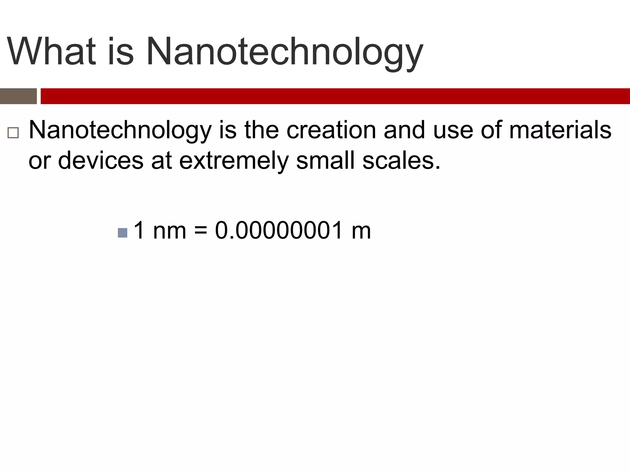
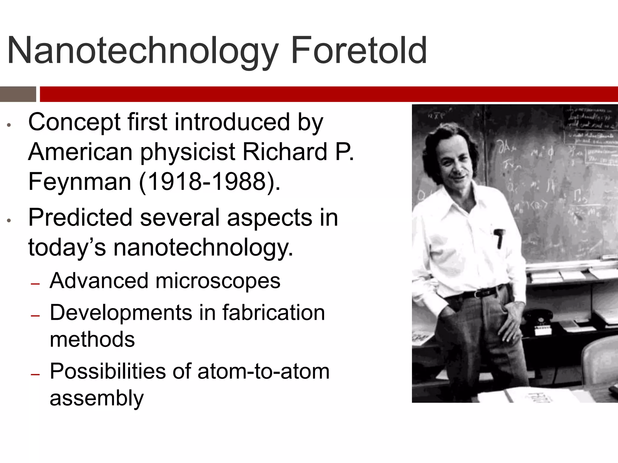
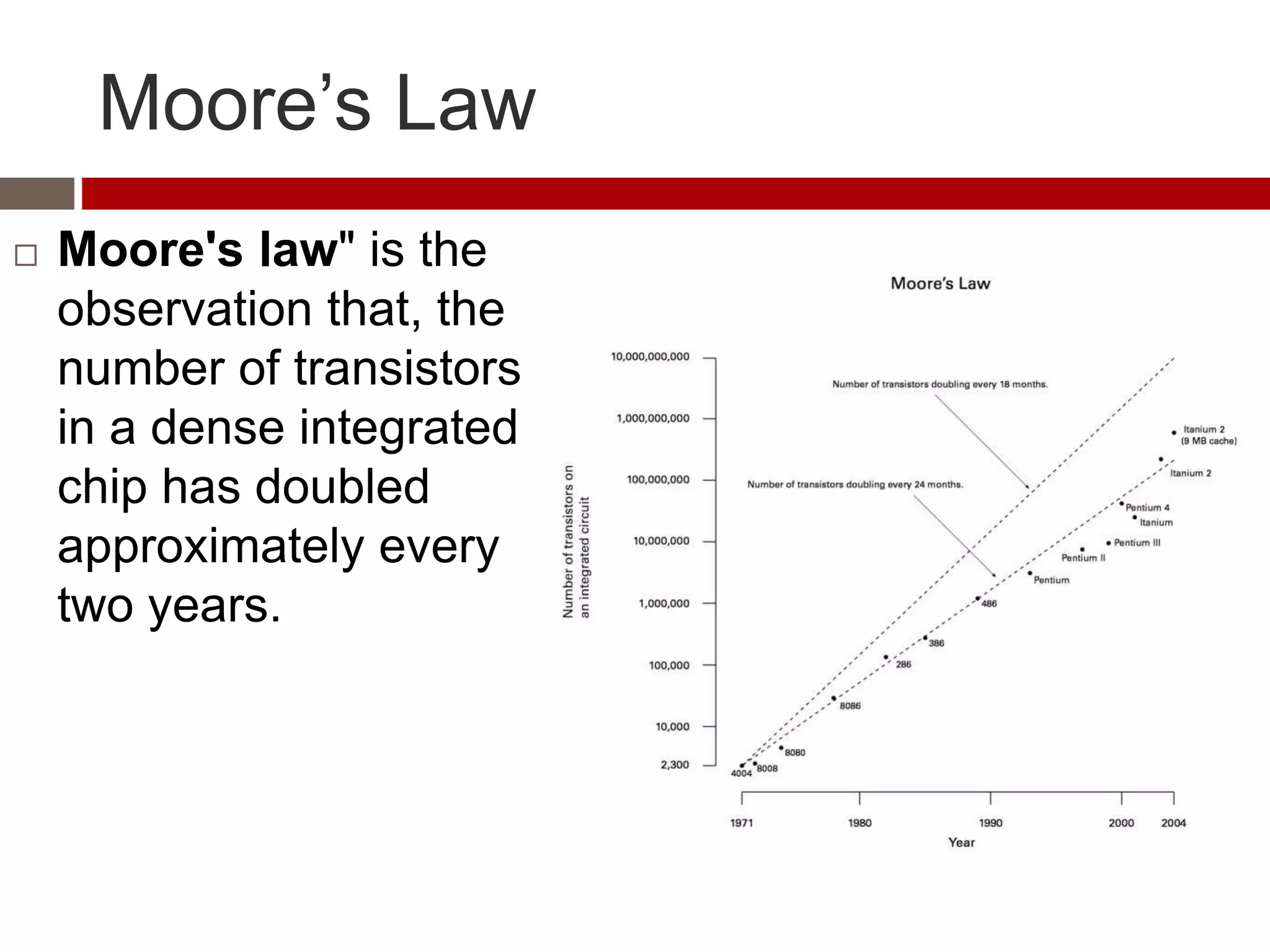
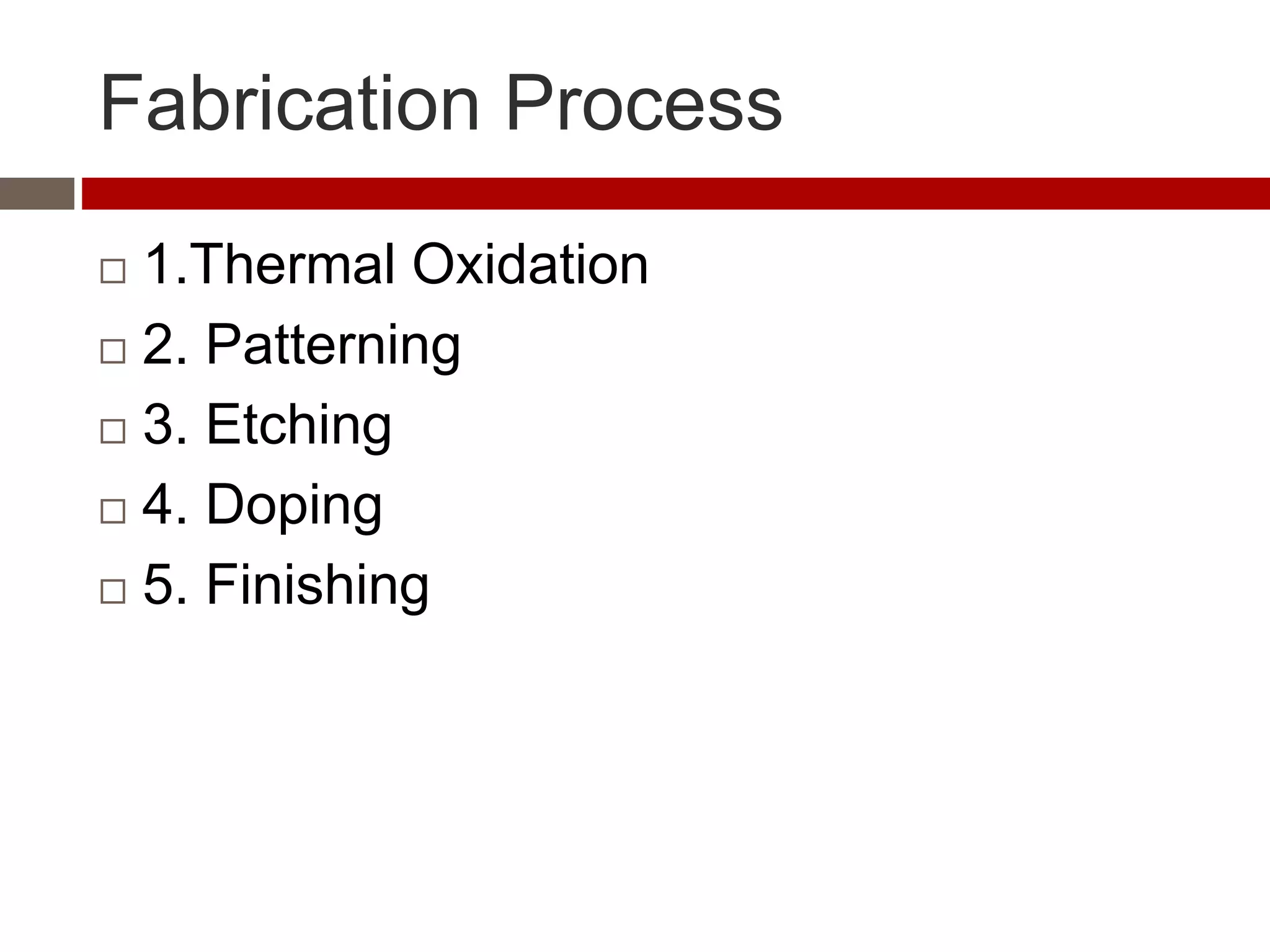
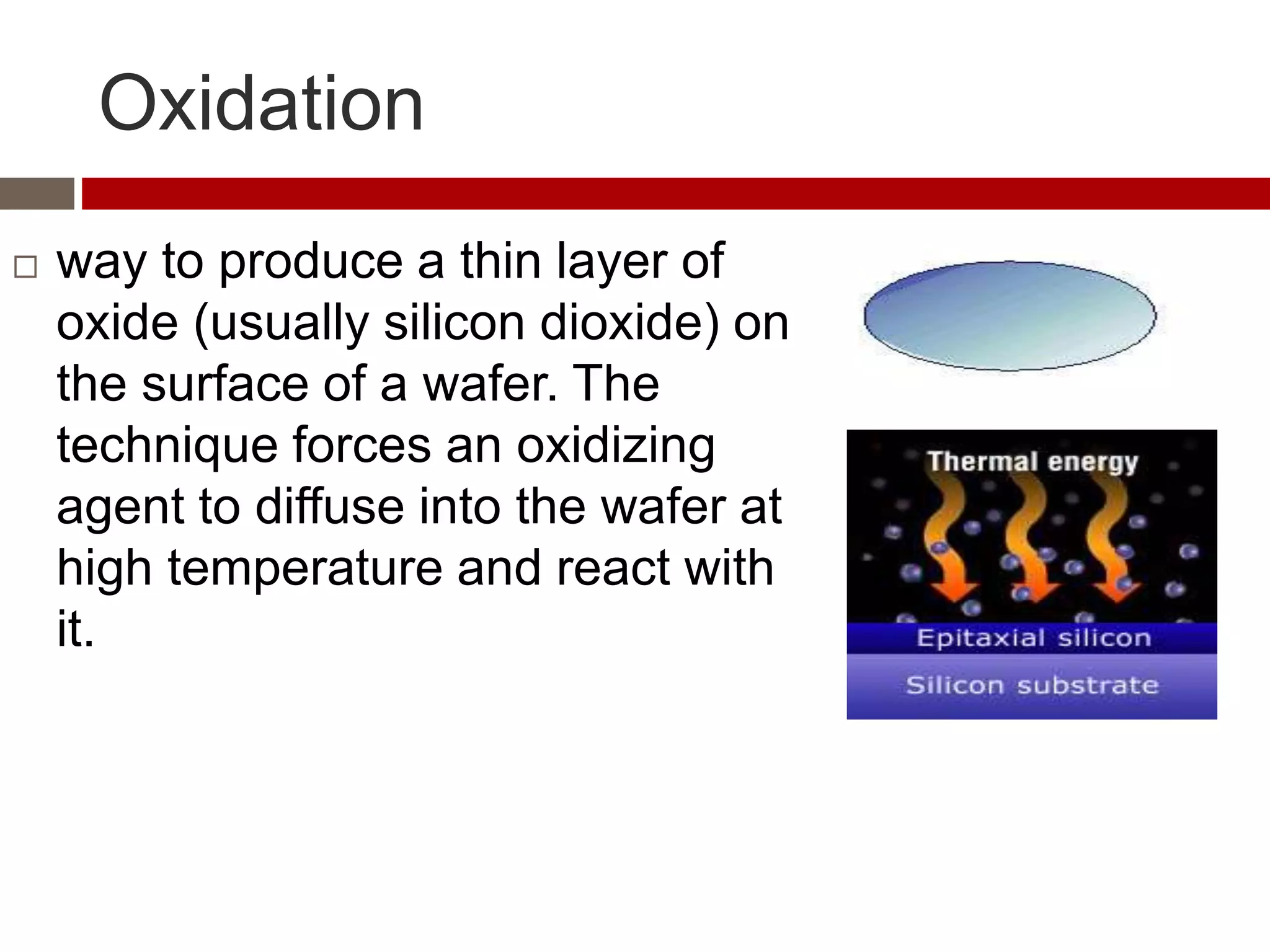
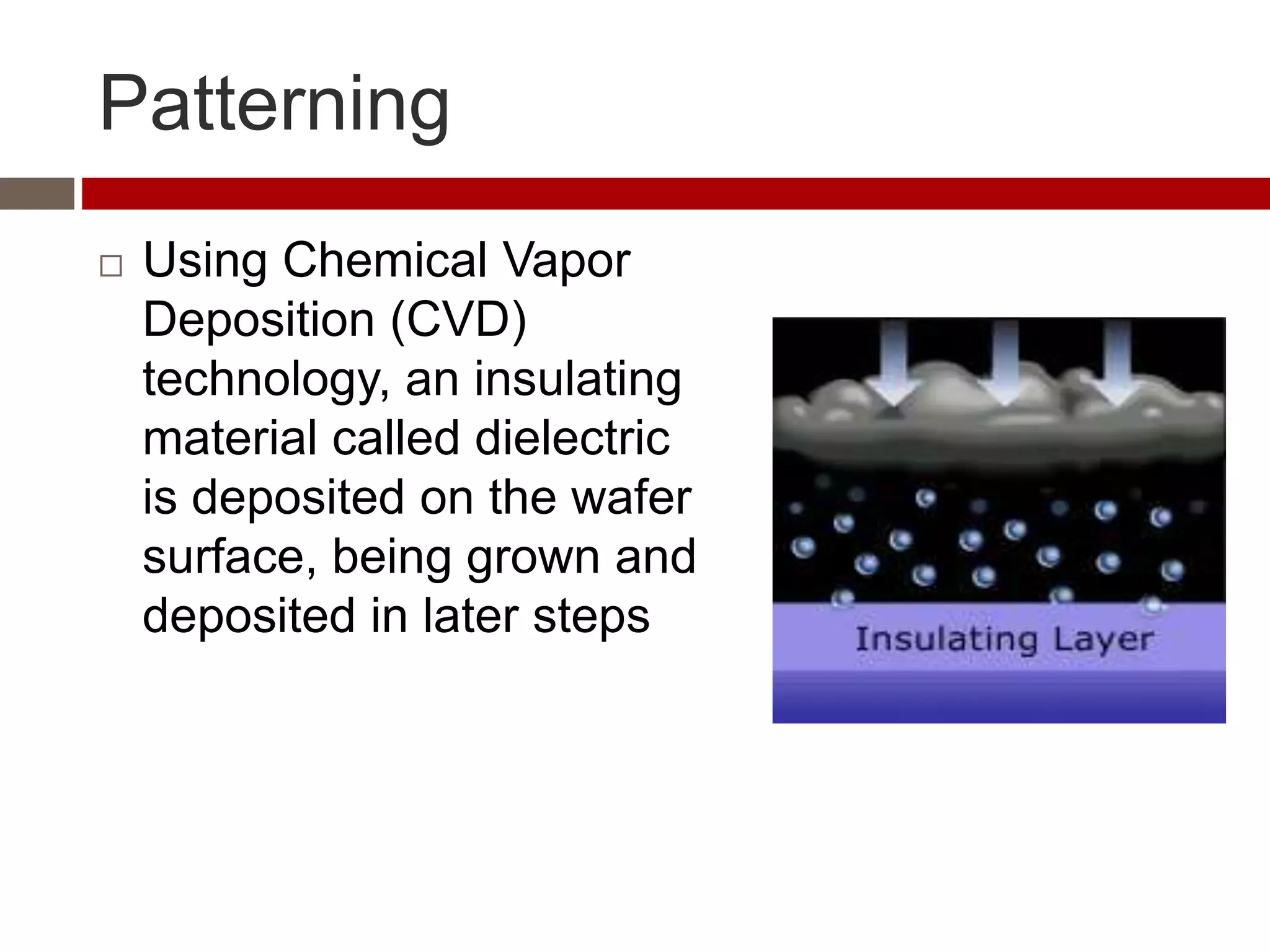
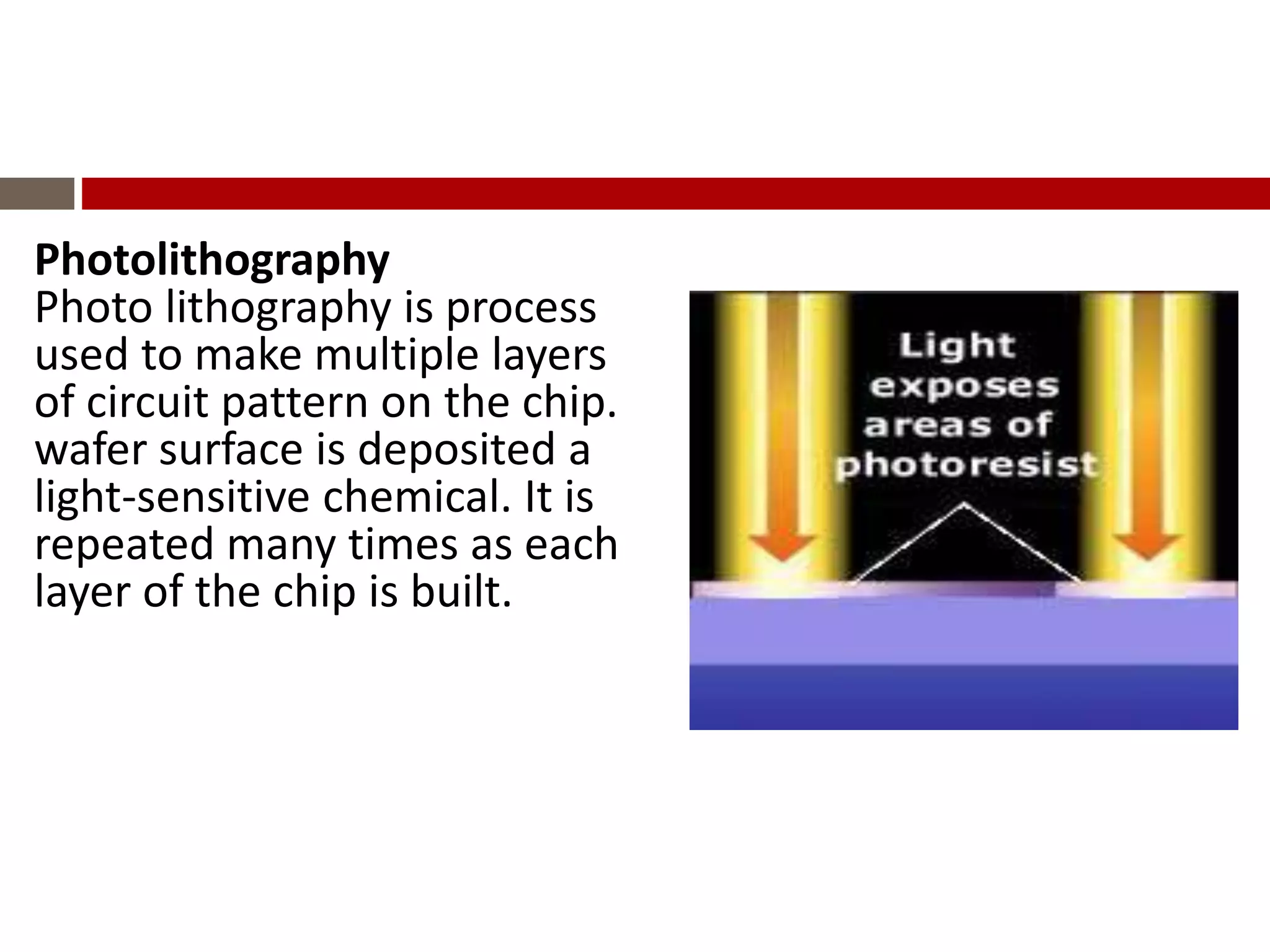
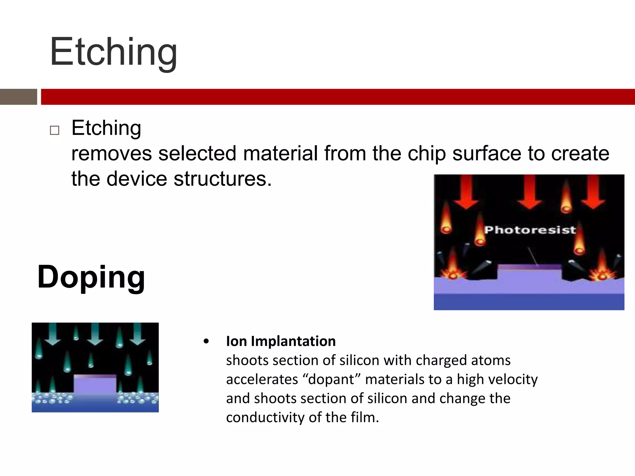
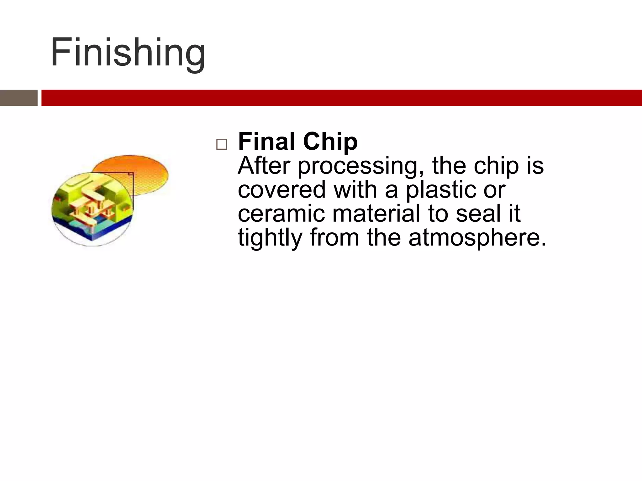
This document discusses nanotechnology and chip fabrication. It begins with an introduction to nanotechnology, noting that it involves creating materials and devices at extremely small scales of 1 nm or less. It then covers the history of nanotechnology, predicting its development by Richard Feynman. The document outlines the fabrication process for chips, including thermal oxidation, patterning, etching, doping, and finishing. It provides details on each step, such as how chemical vapor deposition is used for patterning and photolithography makes circuit patterns on chips. The summary concludes by mentioning Moore's Law about transistors doubling every two years.
2. Group Members
Khan, Bayzid [ 11-19915-3]
Hasan, Md. Mahedi [12-21498-2]
Mujaheden Chy, S.M. Emam-Ul [12-22708-3]
3. In this presentation
Concept and History of Nanotechnology.
Why Nanotechnology ?
Nanotechnology Foretold
Fabrication Process
4. What is Nanotechnology
Nanotechnology is the creation and use of materials
or devices at extremely small scales.
1 nm = 0.00000001 m
5. Nanotechnology Foretold
• Concept first introduced by
American physicist Richard P.
Feynman (1918-1988).
• Predicted several aspects in
today’s nanotechnology.
– Advanced microscopes
– Developments in fabrication
methods
– Possibilities of atom-to-atom
assembly
6. Moore’s Law
Moore's law" is the
observation that, the
number of transistors
in a dense integrated
chip has doubled
approximately every
two years.
8. Oxidation
way to produce a thin layer of
oxide (usually silicon dioxide) on
the surface of a wafer. The
technique forces an oxidizing
agent to diffuse into the wafer at
high temperature and react with
it.
9. Patterning
Using Chemical Vapor
Deposition (CVD)
technology, an insulating
material called dielectric
is deposited on the wafer
surface, being grown and
deposited in later steps
10. Photolithography
Photo lithography is process
used to make multiple layers
of circuit pattern on the chip.
wafer surface is deposited a
light-sensitive chemical. It is
repeated many times as each
layer of the chip is built.
11. Etching
Etching
removes selected material from the chip surface to create
the device structures.
• Ion Implantation
shoots section of silicon with charged atoms
accelerates “dopant” materials to a high velocity
and shoots section of silicon and change the
conductivity of the film.
Doping
12. Finishing
Final Chip
After processing, the chip is
covered with a plastic or
ceramic material to seal it
tightly from the atmosphere.