Downloaded 500 times

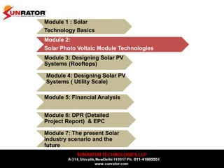
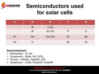
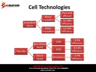
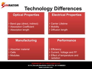
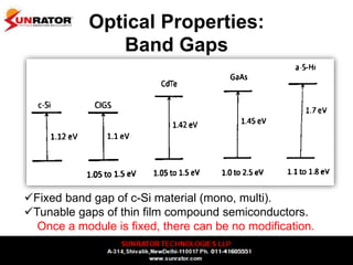
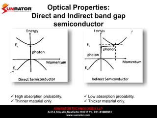
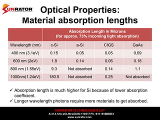
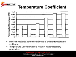
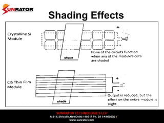


This document summarizes and compares different solar photovoltaic module technologies, including crystalline silicon, thin film technologies, and the differences between them. It covers optical properties like band gap and absorption coefficients, electrical properties like carrier lifetime and mobility, manufacturing processes, and performance metrics like efficiency, temperature coefficients, and response to shading. The key solar cell material technologies discussed are mono-crystalline silicon, multi-crystalline silicon, cadmium telluride (CdTe), copper indium gallium selenide (CIGS), and amorphous silicon.


