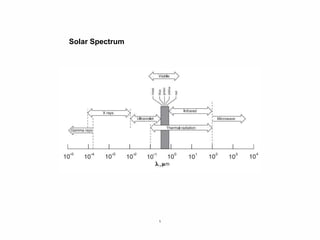
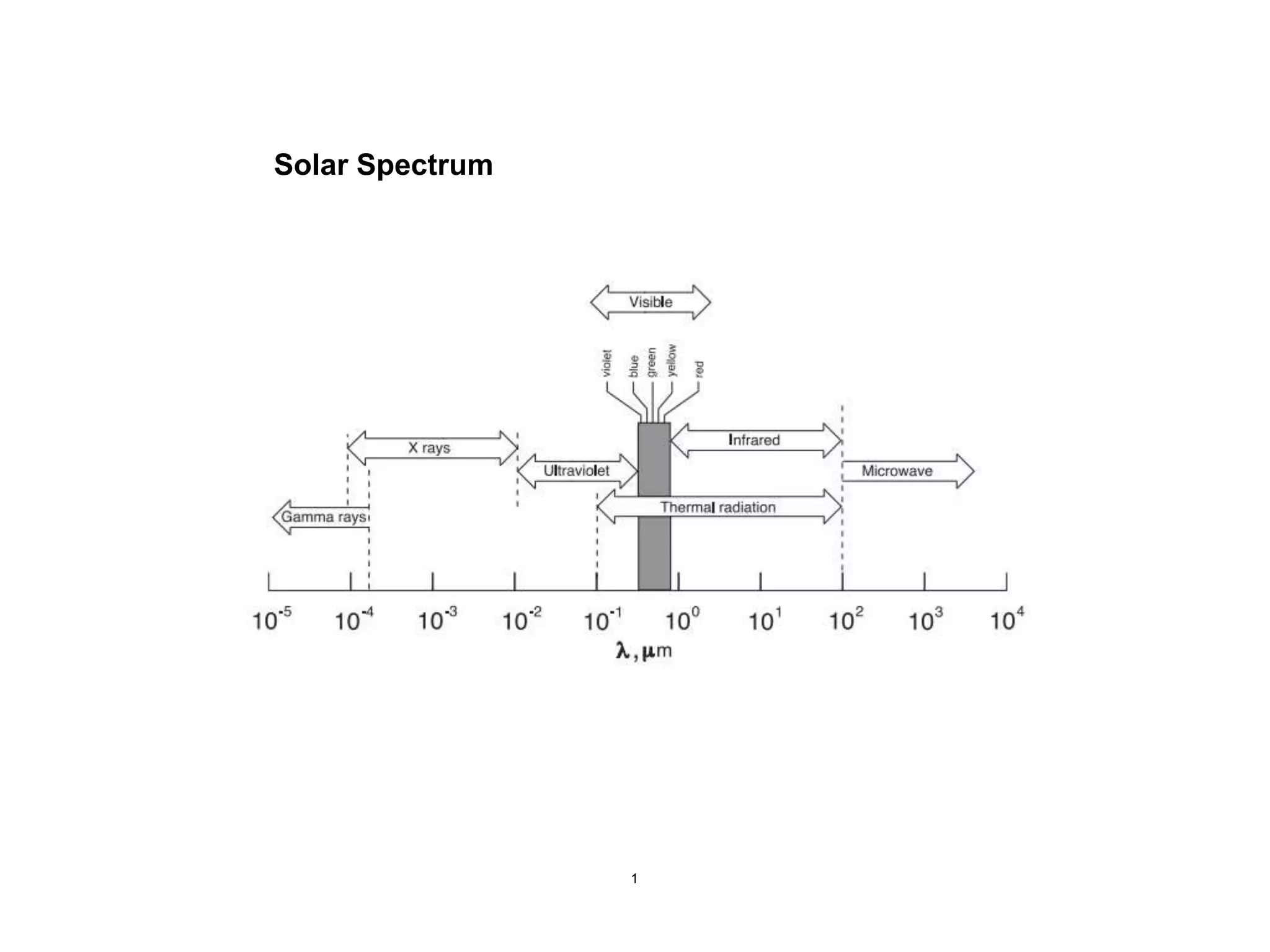
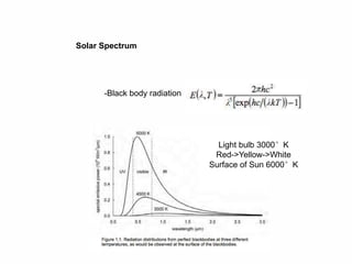
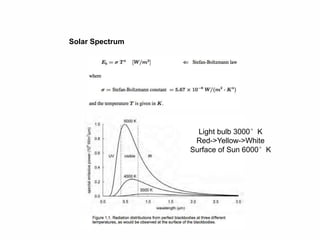
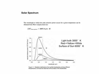
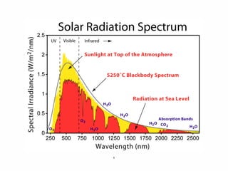
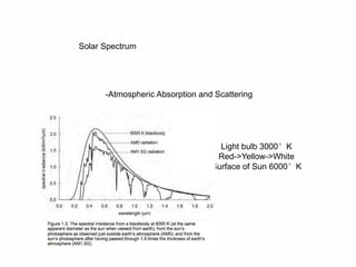
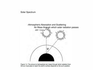
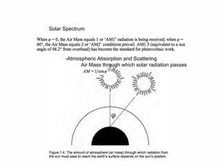
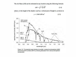
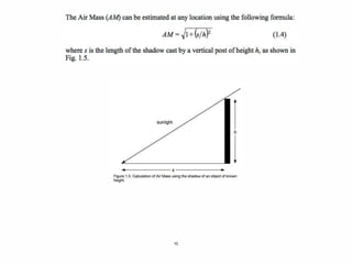
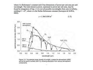
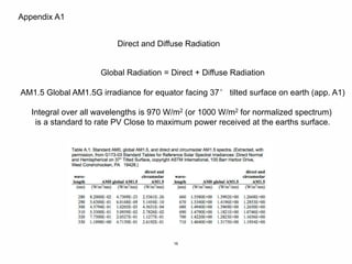
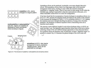
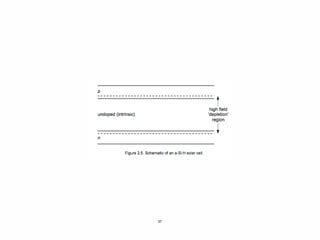
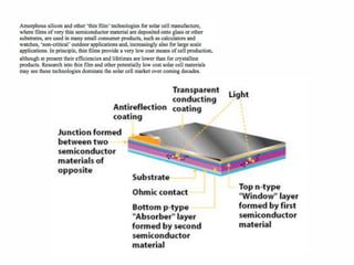
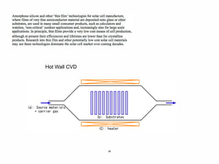
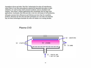
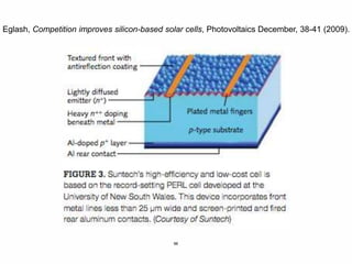
1
Solar Spectrum
2
Solar Spectrum
-Black body radiation
Light bulb 3000°K
Red->Yellow->White
Surface of Sun 6000°K
3
Solar Spectrum
-Black body radiation
Light bulb 3000°K
Red->Yellow->White
Surface of Sun 6000°K
4
Solar Spectrum
-Black body radiation
Light bulb 3000°K
Red->Yellow->White
Surface of Sun 6000°K
5
Solar Spectrum
-Atmospheric Absorption and Scattering
Light bulb 3000°K
Red->Yellow->White
Surface of Sun 6000°K
6
Solar Spectrum
-Atmospheric Absorption and Scattering
Light bulb 3000°K
Red->Yellow->White
Surface of Sun 6000°K
7
Solar Spectrum
-Atmospheric Absorption and Scattering
Air Mass through which solar radiation passes
8
Solar Spectrum
-Atmospheric Absorption and Scattering
Air Mass through which solar radiation passes
9
10
11
12
30% lost to Rayleigh Scattering λ-4 (blue sky/orange sunset)
Scattering by aerosols (Smoke, Dust and Haze S.K. Friedlander)
Absorption: Ozone all below 0.3 µm, CO2, O2, H2O
13
10% added to AM1 for clear skies by diffuse component
Increases with cloud cover
½ lost to clouds is recovered in diffuse radiation
14
15
16
Direct and Diffuse Radiation
Global Radiation = Direct + Diffuse Radiation
AM1.5 Global AM1.5G irradiance for equator facing 37° tilted surface on earth (app. A1)
Integral over all wavelengths is 970 W/m2 (or 1000 W/m2 for normalized spectrum)
is a standard to rate PV Close to maximum power received at the earths surface.
Appendix A1
17
Standard Spectrum is compared to Actual Spectrum for a site
Solar Insolation Levels
March
June
September
December
18
Cape
Town/Melbourne/Chattanooga
Gibraltar/Beirut/Shanghai
19
Appendix B
20
21
22
Need:
-Global radiation on a horizontal surface
-Horizontal direct and diffuse components of global value
-Estimate for tilted plane value
Equations given in Chapter on Sunlight
Peak sun hours reduces a days variation to a fixed number of peak hours for calculations
SSH = Sunshine Hours
Total number of hours above 210 W/m2 for a month
Equations in Chapter 1 to convert SSH to a useful form.
23
Estimates of Diffuse Component
Clearness Index KT = diffuse/total
This is calculaed following the algorithm given in the chapter
Use number of sunny and cloudy days to calculate diffuse and direct insolation
Described in the book
24
Tilted Surfaces
PV is mounted at a fixed tilt angle
25
Sunny versus Cloudy
26
27
Calculation for
Optimal Tilt Angle
Given in the Chapter
28
1
cosq
29
P-N Junctions and Commercial Photovoltaic Devices
Chapter 2
30
31
32
Czochralski Process
33
34
35
36
37
38
39
Hot Wall CVD
40
Plasma CVD
41
42
43
Market Share
CIS= Copper Indium Gallium Selenide
a-Si= Amorphous Silicon
Ribbon= Multicrystalline Silicon from
Molten Bath
CdTe= Cadium Telluride/Cadmium Sulfid
Mono = Monocrystalline Silicaon
Multi= Muticrystalline Silicon
44
Positive ion cores
Negative ion cores
Depleted of
Free Carriers
http://www.asdn.net/asdn/physics/p-n-junctions.shtml
45
Carrier Generation
Carrier Recombination
Carrier Diffusion
Carrier Drift in Depletion Region
due to inherent field
On average a minority carrier
Travels the diffusion length
Before recombining
This is the diffusion current
Carriers in the depletion region
Are carried by the electric field
This is the drift current
In equilibrium drift = diffusion
Net current = 0
46
47
I–V characteristics of a p–n junction diode (not to scale—the
current in the reverse region is magnified compared to the
forward region, resulting in the apparent slope discontinuity at
the origin; the actual I–V curve is smooth across the origin).
http://en.wikipedia.org/wiki/Diode
48
I–V characteristics of a p–n junction diode (not to scale—the
current in the reverse region is magnified compared to the
forward region, resulting in the apparent slope discontinuity at
the origin; the actual I–V curve is smooth across the origin).
http://en.wikipedia.org/wiki/Diode
49
Electron-hole pair
-Generation
-Recombination
Carrier lifetime (1 µs)
Carrier diffusion length (100-300 µm)
50
51
N=photon flux
α=abs. coef.
x=surface depth
G=generation rate
e-h pairs
52
N=photon flux
α=abs. coef.
x=surface depth
G=generation rate
e-h pairs
53
54
55
I0 is dark saturation current
q electron charge
V applied voltage
k Boltzmann Constant
T absolute temperature
56
N=photon flux
α=abs. coef.
x=surface depth
G=generation rate
e-h pairs
At x = 0 G =αN
Function is G/Gx=0 = exp(-αx)
Electrons absorb the band gap energy
57
Diode Equation Photovoltaic Equation
Silicon Solar Cell
58
Efficiency of Light Conversion to e-h pair
59
Short Circuit Current, V = 0
60
Inefficiency of the e-h pair formation and collection process
61
Voc drops in T because I0 increases
Open Circuit Voltage
http://pvcdrom.pveducation.org/CELLOPER/TEMP.HTM
62
Maximum Power
63
Effect of Shunt Resistance on fill factor
http://www.pv.unsw.edu.au/information-for/online-students/online-
courses/photovoltaics-devices-applications/syllabus-details
Fill Factor
64
Effect of Shunt Resistance on fill factor
http://www.pv.unsw.edu.au/information-for/online-students/online-
courses/photovoltaics-devices-applications/syllabus-details
Fill Factor
65
66
Spectral Response
Quantum Efficiency = number of e-h pairs made per photon
Band gap determines when this is greater than 0
Need band gap between 1.0 and 1.6 eV to match solar spectrum
Si 1.1 eV Cd 1.5 eV
67
Issues effecting quantum efficiency
Absorption spectrum
Band Gap
Spectral Responsivity = Amps per Watt of Incident Light
Short wavelengths => loss to heat
Long wavelengths => weak absorption/finite diffusion length
68
69
Chapter 4 Cell Properties
Lab Efficiency ~ 24%
Commercial Efficiency ~ 14%
Lab processes are not commercially viable
C is Cost of Generated Electricity
ACC Capital Cost
O&M is Operating and Maintenance Cost
t is year
E is energy produced in a year
r is discount rate interest rate/(i.r. + 1)
70
C is Cost of Generated Electricity
ACC Capital Cost
O&M is Operating and Maintenance Cost
t is year
E is energy produced in a year
r is discount rate interest rate/(i.r. + 1)
Increased Efficiency increases E and lowers C.
Can also reduce ACC, Installation Costs, Operating Costs
To improve C
For current single crystal or polycrystalline silicon technology
Wafer costs account for ½ of the module cost.
½ is marketing, shipping, assembly etc.
We can adresss technically only the efficiency E
71
Solar Cell Module Efficiency
Optical Losses Due to Reflection
1) Minimize surface contact area
(increases series resistance)
2) Antireflection coatings
¼ wave plate
transparent coating of thickness
d1 and refractive index n1
d1 = λ0/(4n1)
n1 = sqrt(n0n2)
2) Surface Texturing
Encourage light to bounce
back into the cell.
3) Absorption in rear cell contact.
Desire reflection but at
Random angle for internal
reflection
72
d1 = λ0/(4n1) n1 = sqrt(n0n2)
73
74
Dobrzanski, Drygala, Surface Texturing in Materials and Manufacturing Engineering, J. Ach. In Mat. And Manuf. Eng.
31 77-82 (2008).
75
76
Reduce recombination at contacts by heavily doping near contacts
77
Recombination Losses
Red
Blue
78
Recombination Losses
79
Recombination Losses
80
81
82
83
Bulk & Sheet Resistivity
Sheet Resistivity
84
Eglash, Competition improves silicon-based solar cells, Photovoltaics December, 38-41 (2009).
85
SunPower San Jose, CA
20% eficiency from Czochralski silicon
86
Eglash, Competition improves silicon-based solar cells, Photovoltaics December, 38-41 (2009).
87
Suntech, Wuxi, China
multi crystalline cast silicon
Efficiency 16.5%
Cost $1.50 per watt
88
Eglash, Competition improves silicon-based solar cells, Photovoltaics December, 38-41 (2009).
89
90
91

AppliedPhotoVoltaics.ppt