This document provides information about semiconductors and semiconductor devices. It includes:
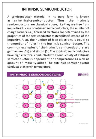
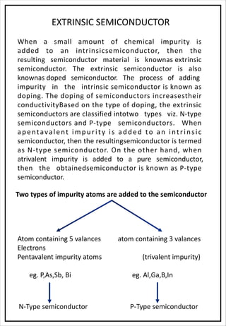
1. Definitions of intrinsic and extrinsic semiconductors and how they are doped with impurities.
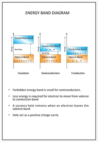
2. Descriptions of the energy band diagram and mass action law governing semiconductors.
3. Explanations of how PN junction diodes work under forward and reverse bias, including the formation of the depletion region and potential barrier.
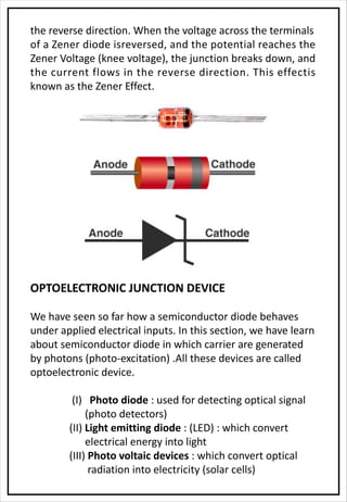
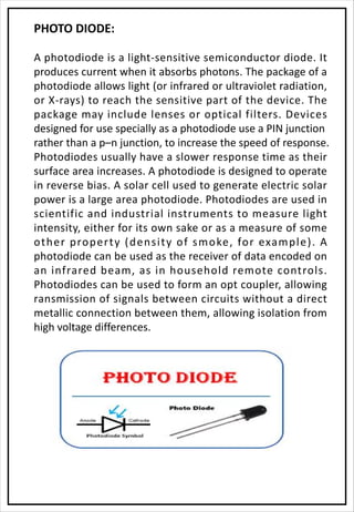
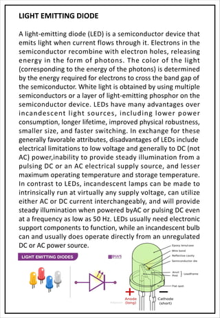
4. Discussions of different types of diodes like Zener diodes and optoelectronic devices like photodiodes and light emitting diodes.
Semiconductors are materials that have electrical conductivity between conductors such as most metals and nonconductors or insulators like ceramics. How much electricity a semiconductor can conduct depends on the material and its mixture content.
Semiconductors can be insulators at low temperatures and conductors at high temperatures. As they are used in the fabrication of electronic devices, semiconductors play an important role in our lives.
In this PPT we will study about the Transistor , symbol of transistor , types of transistor, operation of transistor , configurations of transistor, advantages of transistor and limitations of transistor.
#physicspptclub #In this video we will study about the Transistor , symbol of transistor , types of transistor, operation of transistor , configurations of transistor, advantages of transistor and limitations of transistor.
#physicspptclub #physicsexperiments #solid state #magnetism #magneticmaterial #presentation #education #physicsfacts #scienceexperiment #presentation #education #physicsfacts #scienceexperiment #quantum #presentation #quantumphysics #bsc #msc #btech #diodecircuits #pnjunctiondiode #physicsfacts #characteristics #education #transistor #pnptransistor #npntransistor #solid state #magnetism #magneticmaterial #presentation #education #physicsfacts #scienceexperiment #presentation #education #physicsfacts #scienceexperiment #quantum #presentation #quantumphysics #bsc #msc #btech #diodecircuits #pnjunctiondiode #physicsfacts #characteristicsis #education #transistor #pnptransistor #npntransistor
Semiconductor Diode :
What is Semiconductor Diode?
How is it Work?
What are the Types?
Current Flow in Forward And Reverse Bios?
What is Light Emitting Diode (LED)?
What is Zener Diode?
and in aditional :
P-N Junction and its formation
Formation of Depletion Layer
External Biasing of P-N Junction
V-I Characteristics of P-N Junction
Zener Breakdown
Avalanche Breakdown
Comparison between Zener and Avalanche Breakdown
GSM Based climate Monitoring System for AgricultureLokesh K N
Design of GSM based weather monitoring system useful for agriculture consists of different sensors such as temperature, humidity and soil moisture. Sensors are used to measure moisture content of soil, temperature level and humidity level. The Arduino Uno receives the data from the various sensor and transmit it to the GSM module. The GSM module send the information to formers via Short Message Service (SMS).
The implementation of this system in agriculture for future will not only save the time, money and water but also increase the productivity of crops and improves the growth of the plants.
The future iteration will include data collection at base station and incorporation of additional remote station directly controls irrigation systems. Wireless transmission of the output data to the user with the help of using ZigBee or Bluetooth. In this way the agriculture monitoring system helps the formers in the form of improving their yields.
Express Technologies is one of the Top Electronic Components Distributors
that brings exclusive range of electronic components like transistors, rabbit semiconductor microcontrollers, relays and more in one location.
Seminar report on Flexible Electronics by Sourabh KumarSourabh Kumar
www.androroot.com
Seminar report on Flexible Electronics by Sourabh Kumar
Flexible electronics is a new trend in electronics industry to handle the increasing burden on chips. It is a technology for assembling electronic circuits by mounting electronic devices on flexible plastic substrate. This technology is increasingly being used in a number of applications which benefit from their light weight, favourable dielectric properties, robust, high circuit density and conformable nature. Flexible circuits can be rolled away when not required. To replace glass, plastic substrate must offer properties like clarity, dimensional stability, low coefficient of thermal expansion, elasticity etc. Recent advances in organic and inorganic based electronics proceeds on flexible substrate, offer substantial rewards in terms of being able to develop displays that are thinner , lighter and can be rolled when not in use. This paper will discuss about the properties, preparation methods, applications and challenges in this rapidly growing industry.
Keywords : Electronics, Flexible, Circuits, Silicon, Substrates
Semiconductors are materials which have a conductivity between conductors (generally metals) and nonconductors or insulators (such as most ceramics). Semiconductors can be pure elements, such as silicon or germanium, or compounds such as gallium arsenide or cadmium selenide
Introduction about semiconductors and their integration with nanomaterialAbhay Rajput
1)What is Semiconductor?
2)Use of Semiconductor in different sectors.
3)Manufacturing Process
4)Types
5)Semiconductor Nanomaterial process
6)Properties
Transient Electronics: as per the name defines itself "lasting only for a short time"these devices can very well be used in covert operations where they can simply disappear after serving their purpose.Help in reducing e-waste.
The Development of Nanotechnology in Electronic Devices.pdfCIOWomenMagazine
The existence of nanotechnology in electronic devices helps the functionality of the devices. The weight and power consumption are reduced substantially. Nanotechnology means any technology on the nano-scale which has numerous applications in the world.
A new eliminating EOG artifacts technique using combined decomposition method...TELKOMNIKA JOURNAL
This paper reviews the fabrication technologies of silicon nanowire transistors (SiNWTs) and rapidly development in this area, as this paper presents various types of SiNWT structures, development of SiNWT properties and different applications until nowadays. This research provides a good comparison among fabrication technologies of SiNWTs depending on a new factor DIF, this factor depends on the size of channel and power consumption in channel. As a result of this comparison, the best technology to use in the future to fabricate silicon nano transistors for future ICs is AFM nanolithography.
Semiconductors and their usage in different applicationsexpess-technology
Express Technologies is a one-stop solution to accomplish your needs. It is one of the reliable suppliers that deal in a complete range of electronic components such as diodes, Rabbit Semiconductor Microcontroller, relays, and many more.
Hierarchical Digital Twin of a Naval Power SystemKerry Sado
A hierarchical digital twin of a Naval DC power system has been developed and experimentally verified. Similar to other state-of-the-art digital twins, this technology creates a digital replica of the physical system executed in real-time or faster, which can modify hardware controls. However, its advantage stems from distributing computational efforts by utilizing a hierarchical structure composed of lower-level digital twin blocks and a higher-level system digital twin. Each digital twin block is associated with a physical subsystem of the hardware and communicates with a singular system digital twin, which creates a system-level response. By extracting information from each level of the hierarchy, power system controls of the hardware were reconfigured autonomously. This hierarchical digital twin development offers several advantages over other digital twins, particularly in the field of naval power systems. The hierarchical structure allows for greater computational efficiency and scalability while the ability to autonomously reconfigure hardware controls offers increased flexibility and responsiveness. The hierarchical decomposition and models utilized were well aligned with the physical twin, as indicated by the maximum deviations between the developed digital twin hierarchy and the hardware.
Overview of the fundamental roles in Hydropower generation and the components involved in wider Electrical Engineering.
This paper presents the design and construction of hydroelectric dams from the hydrologist’s survey of the valley before construction, all aspects and involved disciplines, fluid dynamics, structural engineering, generation and mains frequency regulation to the very transmission of power through the network in the United Kingdom.
Author: Robbie Edward Sayers
Collaborators and co editors: Charlie Sims and Connor Healey.
(C) 2024 Robbie E. Sayers
Final project report on grocery store management system..pdfKamal Acharya
In today’s fast-changing business environment, it’s extremely important to be able to respond to client needs in the most effective and timely manner. If your customers wish to see your business online and have instant access to your products or services.
Online Grocery Store is an e-commerce website, which retails various grocery products. This project allows viewing various products available enables registered users to purchase desired products instantly using Paytm, UPI payment processor (Instant Pay) and also can place order by using Cash on Delivery (Pay Later) option. This project provides an easy access to Administrators and Managers to view orders placed using Pay Later and Instant Pay options.
In order to develop an e-commerce website, a number of Technologies must be studied and understood. These include multi-tiered architecture, server and client-side scripting techniques, implementation technologies, programming language (such as PHP, HTML, CSS, JavaScript) and MySQL relational databases. This is a project with the objective to develop a basic website where a consumer is provided with a shopping cart website and also to know about the technologies used to develop such a website.
This document will discuss each of the underlying technologies to create and implement an e- commerce website.
CW RADAR, FMCW RADAR, FMCW ALTIMETER, AND THEIR PARAMETERSveerababupersonal22
It consists of cw radar and fmcw radar ,range measurement,if amplifier and fmcw altimeterThe CW radar operates using continuous wave transmission, while the FMCW radar employs frequency-modulated continuous wave technology. Range measurement is a crucial aspect of radar systems, providing information about the distance to a target. The IF amplifier plays a key role in signal processing, amplifying intermediate frequency signals for further analysis. The FMCW altimeter utilizes frequency-modulated continuous wave technology to accurately measure altitude above a reference point.
Industrial Training at Shahjalal Fertilizer Company Limited (SFCL)MdTanvirMahtab2
This presentation is about the working procedure of Shahjalal Fertilizer Company Limited (SFCL). A Govt. owned Company of Bangladesh Chemical Industries Corporation under Ministry of Industries.
Saudi Arabia stands as a titan in the global energy landscape, renowned for its abundant oil and gas resources. It's the largest exporter of petroleum and holds some of the world's most significant reserves. Let's delve into the top 10 oil and gas projects shaping Saudi Arabia's energy future in 2024.
Forklift Classes Overview by Intella PartsIntella Parts
Discover the different forklift classes and their specific applications. Learn how to choose the right forklift for your needs to ensure safety, efficiency, and compliance in your operations.
For more technical information, visit our website https://intellaparts.com
NUMERICAL SIMULATIONS OF HEAT AND MASS TRANSFER IN CONDENSING HEAT EXCHANGERS...ssuser7dcef0
Power plants release a large amount of water vapor into the
atmosphere through the stack. The flue gas can be a potential
source for obtaining much needed cooling water for a power
plant. If a power plant could recover and reuse a portion of this
moisture, it could reduce its total cooling water intake
requirement. One of the most practical way to recover water
from flue gas is to use a condensing heat exchanger. The power
plant could also recover latent heat due to condensation as well
as sensible heat due to lowering the flue gas exit temperature.
Additionally, harmful acids released from the stack can be
reduced in a condensing heat exchanger by acid condensation. reduced in a condensing heat exchanger by acid condensation.
Condensation of vapors in flue gas is a complicated
phenomenon since heat and mass transfer of water vapor and
various acids simultaneously occur in the presence of noncondensable
gases such as nitrogen and oxygen. Design of a
condenser depends on the knowledge and understanding of the
heat and mass transfer processes. A computer program for
numerical simulations of water (H2O) and sulfuric acid (H2SO4)
condensation in a flue gas condensing heat exchanger was
developed using MATLAB. Governing equations based on
mass and energy balances for the system were derived to
predict variables such as flue gas exit temperature, cooling
water outlet temperature, mole fraction and condensation rates
of water and sulfuric acid vapors. The equations were solved
using an iterative solution technique with calculations of heat
and mass transfer coefficients and physical properties.
2. This Is To Certify That Of B.sc Semester 5th Of
Doranda college Completetd her Project Report On The Topic Data
Processing Circuit . Under The Guidance Of
3. The hard Work Apart, it’s not just a will being one to put forth the
outcomes of it. There are many hands in to put up when to get the
things modeled and making them in a view to count.
I am very grateful to the department of physics< Doranda College
Ranchi , for providing me a project. it was very enlightening for me. i
had finished in learning the type of work.
At a very outside , i am obliged to dr, V.P Verma principal, Doranda
College Ranchi Unoiversity , ranchi for giving me all desirable
facilities to start my work. I am deeply indebted to prof. J.P Roy (rtd).
Mr. N.K Sharma Under whose supervision i have been able to
accomplished the project.
I extend my sincere thanks to all the person of the department and
also my frinds who helped me in the preperation of my project.
priya kumari
roll no:-
department of B.sc , doranda College
Session:- 2020- 2023
5. The material whose electrical conductivity lies between those of
conductor andinsulator are known as semiconductor.
• Silicon 1.1Ev
• Germanium 0.7Ev
• Cadmium Sulphide 2.4Ev
§ Semiconductors are crystalline or amorphous solids with
distinct electrical characteristics
§ They are of high resistance higher than typical resistance
materials but still of much lower resistance than insulators
§ Their resistance decreases as their temperature increases ,
which is behavior opposite to that of a metal
§ Silicon is the most widely used semiconductor
DISCOVERY
Whenever We will learn about the history of electricity and
electronics We will find that a lot of the ground breaking
work was done in the 19th centuay .the situation is no
different for semiconductors Tariq siddiqui is generally
acknowledge is one of the first experimenters to notice
semiconductor properties.
6. The objective of semiconductor technology is to revolutionize
the world of electronics by creating and developing electronic
devices that can efficiently control the flow of electrical current.
Semiconductors, as their name suggests, are materials with
properties that allow them to conduct electricity under certain
conditions and act as insulators under others. This unique
characteristic makes them ideal for manipulating and controlling
electrical signals.
The primary objective of semiconductor technology is to harness
these properties to design and manufacture components such as
transistors, diodes, and integrated circuits. These components
are the fundamental building blocks for various electronic
devices that we rely on in our daily lives. By continuously
improving the performance, functionality, size, energy efficiency,
and cost of these devices, semiconductor technology aims to
transform the way we communicate, compute, entertain, travel,
receive healthcare, and generate renewable energy.
One of the main goals of semiconductor technology is to provide
improved performance in electronic devices. This involves
developing faster and more powerful processors, memory chips,
and sensors that can handle complex tasks and deliver seamless
user experiences. By constantly pushing the boundaries of what
is possible, semiconductor technology enables advancements in
artificial intelligence, virtual reality, augmented reality, and other
emerging technologies.
7. Another objective is to increase functionality in electronic devices.
This includes integrating multiple functions into a single chip,
enabling devices to perform a wide range of tasks while
occupying less space. For example, smartphones now combine
the capabilities of a phone, camera, music player, GPS navigator,
and more into one compact device.
Semiconductor technology also aims to reduce the size of
electronic devices. This allows for more portable and wearable
gadgets that can be easily carried or worn. The miniaturization of
components is made possible by advancements in semiconductor
manufacturing techniques such as photolithography and
nanotechnology.
Enhancing energy efficiency is another crucial objective of
semiconductor technology. By reducing power consumption and
heat generation in electronic devices, semiconductors enable
longer battery life and contribute to a greener and more
sustainable future. This is particularly important in applications
such as electric vehicles and renewable energy systems, where
energy efficiency plays a significant role.
Lastly, semiconductor technology strives to lower costs in the
production of electronic devices. Through continuous innovation
and economies of scale, semiconductors have become more
affordable, making electronic devices accessible to a wider range
of people around the world. This has led to the democratization
of technology and the proliferation of smartphones, tablets, and
other electronic gadgets in both developed and developing
countries.
In conclusion, the objective of semiconductor technology is to
create and develop electronic devices that can efficiently control
the flow of electrical current. By harnessing the unique
properties of semiconductors, this technology aims to provide
improved performance, increased functionality, reduced size,
enhanced energy efficiency, and lower costs in a wide range of
applications. Through continuous innovation and advancements,
semiconductor technology has revolutionized the world of
electronics and continues to shape our modern society.
8. The materials commonly employed in
semiconductor technology, with a focus on
their properties, fabrication methods, and
applications.
1. Silicon (Si):
Silicon is the most widely used material in semiconductor
technology due to its abundance, excellent electrical
properties, and compatibility with existing manufacturing
processes. It possesses a bandgap of approximately 1.1 eV,
making it suitable for both electronic and photonic
applications. Silicon-based semiconductors are primarily
fabricated through the Czochralski or float-zone methods.
2. III-V Compound Semiconductors:
III-V compound semiconductors are composed of elements
from groups III and V of the periodic table, such as gallium
arsenide (GaAs), indium phosphide (InP), and gallium nitride
(GaN). These materials exhibit superior electron mobility, high
carrier concentrations, and wide bandgaps, enabling efficient
optoelectronic devices. III-V semiconductors are commonly
grown using molecular beam epitaxy (MBE) or metal-organic
chemical vapor deposition (MOCVD) techniques.
3. II-VI Compound Semiconductors:
II-VI compound semiconductors, such as cadmium sulfide
(CdS) and zinc selenide (ZnSe), are composed of elements
from groups II and VI. They possess unique optical properties,
including a wide range of direct bandgaps suitable for light-
emitting devices. II-VI semiconductors are typically grown
using MBE or metal-organic vapor phase epitaxy (MOVPE)
techniques.
9. 4. Organic Semiconductors:
Organic semiconductors are composed of carbon-based
molecules or polymers. These materials offer advantages
such as flexibility, low-cost fabrication, and compatibility with
large-area processing techniques. Organic semiconductors
find applications in organic light-emitting diodes (OLEDs),
organic photovoltaics (OPVs), and organic field-effect
transistors (OFETs). Solution-based methods, such as spin-
coating or inkjet printing, are commonly employed for their
fabrication.
5. Perovskite Semiconductors:
Perovskite semiconductors, such as methylammonium lead
iodide (CH3NH3PbI3), have gained significant attention in
recent years due to their exceptional photovoltaic properties.
These materials exhibit high carrier mobility, long carrier
diffusion lengths, and tunable bandgaps. Perovskite solar
cells are typically fabricated using solution-based techniques
like spin-coating or vapor-assisted deposition.
The choice of semiconductor material is critical in
determining the performance and functionality of electronic
and optoelectronic devices. Silicon, III-V compound
semiconductors, II-VI compound semiconductors, organic
semiconductors, and perovskite semiconductors each offer
unique properties and fabrication methods suited for specific
applications. Understanding the characteristics and
applications of these materials is essential for advancing
semiconductor technology and enabling innovative devices in
various fields
10. ENERGY BAND DIAGRAM
• Forbidden energy band is small for semiconductors .
• Less energy is required for electron to move from valence
to conduction band
• A vacancy hole remains when an electron leaves the
valence band
• Hole act as a positive charge carrie
11. INTRINSIC SEMICONDUCTOR
A semiconductor material in its pure form is known
as an intrinsicsemiconductor. Thus, the intrinsic
semiconductors are chemically pure, i.e.they are free from
impurities.In case of intrinsic semiconductors, the number of
charge carriers, i.e., holesand electrons are determined by the
properties of the semiconductor materialitself instead of the
impurity. Also, the number of free electrons is equal to
thenumber of holes in the intrinsic semiconductor. The
common examples of theintrinsic semiconductors are
germanium (Ge) and silicon (Si).The extrinsic semiconductors
have high electrical conductivity.The conductivity of extrinsic
semiconductor is dependent on temperature as well as
amount of impurity added.The extrinsic semiconductor
conducts at 0 Kelvin temperature.
12. EXTRINSIC SEMICONDUCTOR
When a small amount of chemical impurity is
added to an intrinsicsemiconductor, then the
resulting semiconductor material is knownas extrinsic
semiconductor. The extrinsic semiconductor is also
knownas doped semiconductor. The process of adding
impurity in the intrinsic semiconductor is known as
doping. The doping of semiconductors increasestheir
conductivityBased on the type of doping, the extrinsic
semiconductors are classified intotwo types viz. N-type
semiconductors and P-type semiconductors. When
apentavalent impurity is added to an intrinsic
semiconductor, then the resultingsemiconductor is termed
as N-type semiconductor. On the other hand, when
atrivalent impurity is added to a pure semiconductor,
then the obtainedsemiconductor is known as P-type
semiconductor.
Two types of impurity atoms are added to the semiconductor
Atom containing 5 valances atom containing 3 valances
Electrons
Pentavalent impurity atoms (trivalent impurity)
eg. P,As,Sb, Bi eg. Al,Ga,B,In
N-Type semiconductor P-Type semiconductor
13. N-TYPE SEMICONDUCTOR
The semiconductors which are obtained by introducing
pentavalent impurity atoms are known as N-type
semiconductors . Examples are P, Sb,As, and Bi. These
elements hav 5 electron in their valance sheel.Out of which 4
electron will form covalent bonds with the neighbouring
atoms and the 5th electron will be available as a current
carrier .the impurity atom is thus known as donot tom In N-
type semiconductor current flows due to the movement of
electrons and holes but majority of through electrons.Thus
electon in N –type semiconductor are known as majoriy
charge cariers while holes as minority charge carriers
P-TYPE SEMICONDUCTOR
The semiconductor which are obtained by introducing
trivalent impurity atom are known as P-type semiconductor
Examples are Ga, In, Al and B .these elements have 3 electron
in their valance sheel which will form covalent bond with the
neighbouring atom. The fourth covalent bond will remain
incomplete.A vacancy which exist in the incomplete covalent
bond constitute a hole .The impurity atom is thus known as
acceptor atom In P-type semiconductor current flows due to
movement of electrons and holes but majority of through
holes .Thus holes in P-type semiconductor are known as
majority charge carrierwhile electron as minority charge
carrier
14. MASS ACTION LAW
Addition of n –type impurities decrese the numevr of holes
below a level .Similarly the addition of p-type impurities
decreased the number of electron below a level .It has been
experimentally found that under thermalequilibrium for any
semiconductor the product of no. of holes and the no. of
electrons is constant and independent of amount of doping .
this relation is known as mass action law
Where ne = electron concentration
nh = hole concentration and
ni = intrinsic concentration
BARRIER FORMATION IN P-N JUNCTION
DIODE the holes from p-side diffuses to the n side while the
free electons from n-side diffuses to the p-side.This
movement occurs because od charge density gradient . This
leaves the negative acceptor ions on the p-side and positive
donor ions on the n-side un covered in the vicinity of the
junction .Barrier formation in P-N junction Diode. Thus there
is negative chage on p-side and positive on n –side.This setup
potential difference acriss the junction and hencean internal
electric filed directed from n-side to p-side .Equilibrium is
established when the field become large enough to stop
further diffusion of the majority charge carrier .The region
which become depleted of the mobile charge carrier is called
the depletion region .The potential barrier across the
depletion region is called potential barrier. width of depletion
region depend upon the doping level .The higer the doping
level, thinner will be the depletion region
15. DEPLETION REGION
• It is a region near the p-n junction that is depleted of any
mobile charge carrier
• The depletion region depends upon
1 The type of biasing
2 Extent of doping
POTENTIAL BARRIRE (VB)
Due to accumulation of immobile ion cores in the junction , a
potential difference is developed which prevent the further
movement of majority charge across the junction .
P-N JUNCTION DIODEA
p-n junction consist of wafers of p-type and n type
semiconductors fused together or grown on each other
FORWARD BIASING OF A P-N JUNCTION
(a) A p-n junction is said to be forward biased when p region
is maintained at a higher potential with respect to the n-
region as shown.
(b) When forward biased majority changes carriers in both
the regions are pushed through the junction .The
depletion region’s width decreases andthe junction offers
low resistance , and potential difference across the
junction becomes VB-V
16. REVERSE BIASIG P-N JUNCTION
(a) A p-n junction is said to be reversed biased when its p-
region is maintained at lower potential with respect to its
n-region is as shown
(b) When the junction is reverse biased the majority career
in both the regions are pushed away from the
junction .the depletion region width increase and the
potential difference across the junction becomes VB+V
P-N JUNCTION AS RECTIFIER
Rectification: it is the process of conversion of AC into DC.A
single p-n junction,of two or four p-n junction can be used
for this purpose.
Half wave rectifier : a single p-n junction can be used for half
wave rectifier .It conducts only during alternate half cycle of
the input AC voltage .As a result theoutput voltage does not
change in polarity .The average of the voltage from a half
wave rectifier is low .
Full wave rectifier: It is achieved using two p-n junction .It
conducts for both halves of the cycle .The average voltage of
a full wave rectifier is more than thatof a half wave rectifier ,
for the same rms voltage of AC voltage
SPECIAL PURPOSE p-n JUNCTION DIODES
ZENER DIODE A Zener diode is a heavily doped
semiconductor device that is designed to operate in the
reverse direction. A Zener Diode, also known as a
breakdown diode, is a heavily doped semiconductor device
that is designed to operate in
17. the reverse direction. When the voltage across the terminals
of a Zener diode isreversed, and the potential reaches the
Zener Voltage (knee voltage), the junction breaks down, and
the current flows in the reverse direction. This effectis
known as the Zener Effect.
OPTOELECTRONIC JUNCTION DEVICE
We have seen so far how a semiconductor diode behaves
under applied electrical inputs. In this section, we have learn
about semiconductor diode in which carrier are generated
by photons (photo-excitation) .All these devices are called
optoelectronic device.
(I) Photo diode : used for detecting optical signal
(photo detectors)
(II) Light emitting diode : (LED) : which convert
electrical energy into light
(III) Photo voltaic devices : which convert optical
radiation into electricity (solar cells)
18. PHOTO DIODE:
A photodiode is a light-sensitive semiconductor diode. It
produces current when it absorbs photons. The package of a
photodiode allows light (or infrared or ultraviolet radiation,
or X-rays) to reach the sensitive part of the device. The
package may include lenses or optical filters. Devices
designed for use specially as a photodiode use a PIN junction
rather than a p–n junction, to increase the speed of response.
Photodiodes usually have a slower response time as their
surface area increases. A photodiode is designed to operate
in reverse bias. A solar cell used to generate electric solar
power is a large area photodiode. Photodiodes are used in
scientific and industrial instruments to measure light
intensity, either for its own sake or as a measure of some
other property (density of smoke, for example). A
photodiode can be used as the receiver of data encoded on
an infrared beam, as in household remote controls.
Photodiodes can be used to form an opt coupler, allowing
ransmission of signals between circuits without a direct
metallic connection between them, allowing isolation from
high voltage differences.
19. LIGHT EMITTING DIODE
A light-emitting diode (LED) is a semiconductor device that
emits light when current flows through it. Electrons in the
semiconductor recombine with electron holes, releasing
energy in the form of photons. The color of the light
(corresponding to the energy of the photons) is determined
by the energy required for electrons to cross the band gap of
the semiconductor. White light is obtained by using multiple
semiconductors or a layer of light-emitting phosphor on the
semiconductor device. LEDs have many advantages over
incandescent light sources, including lower power
consumption, longer lifetime, improved physical robustness,
smaller size, and faster switching. In exchange for these
generally favorable attributes, disadvantages of LEDs include
electrical limitations to low voltage and generally to DC (not
AC) power,inability to provide steady illumination from a
pulsing DC or an AC electrical supply source, and lesser
maximum operating temperature and storage temperature.
In contrast to LEDs, incandescent lamps can be made to
intrinsically run at virtually any supply voltage, can utilize
either AC or DC current interchangeably, and will provide
steady illumination when powered byAC or pulsing DC even
at a frequency as low as 50 Hz. LEDs usually need electronic
support components to function, while an incandescent bulb
can and usually does operate directly from an unregulated
DC or AC power source.
20. SOLAR CELL
A solar cell is basically a p-n junction which generates emf
when solar radiation falls on the p-n junction .It works on the
same principle (photo voltaic effect) asthe photodiode,
except that no external bias is applied and the junction area
is kept much larger for solar radiation to be incident because
we are interested in more power.A transistor has three
doped regions forming two p-n junctions between them
there are two types of transistor(i) n-p-n transistor: here two
segments of n –type semiconductor (emitter and collector)
are separated by a segment of p-type semiconductor
(base) .(ii) p-n-p transistor: here two segment of p-type
semiconductor(termed as emitter and collector)are
separated by a segment of n-type semiconductor (termed as
base).A brief description of the three segments of a
transistor is given below:Emitter: this is the segment on one
side of a transistor .It is of moderate size and heavily doped.
It supplies a large number of majority carrier for the current
flow through the transistor
• Base: this is the central segment .It s very thin and lightly
doped
• Collector: this segment collects major portion of the
majority carrier supplied by the emitter.
TRANSISTOR AS A DEVICE
When the transistor is used in the cut off or saturation state
it acts it acts as a switch. On the other hand for using the
transistor as an amplifier it has to operate in the active
region
21. TRANSISTOR AS AN SWITCH
We shall try to understand the operation of the transistor as
a switch by analyzing the behavior of the base-biased
transistor applying Kirchhoff’s voltage rule to the input and
output sides of this circuit we get , V BB = IBRB+VBE And
VCE =VCC - ICRC
TRANSISTOR AS AN AMPLIFIER
For using the transistor as an amplifier we will use the
active region of the V o versus Vi curve .The slope of the
linear part of the curve represent the rate of change of the
output with the input .It is negative because the output is V
cc – Ic R c .That is why as input voltage of the CE amplifier
increases its output voltage decreases and the output is said
to be out of phase with the input
IMPORTANCE OF SEMICONDUCTOR
Semiconductors are a key element of electronic systems,
allowing for developments in communication, computing,
healthcare, military technology, transportation, clean energy,
and a variety of other applications.
Semiconductors, also called integrated circuits (ICs) or
microchips, are made of raw materials like silicon and
germanium. The process is known as doping, where small
add-ons of other elements create fluctuations in how well
the electricity flows
22. Semiconductors are necessary for electronic devices, which
are an integral partof our lives. For example, phones, radios,
TVs, computers, video games, and medical diagnostic
equipment would not exist without semiconductors.
SEMICONDUCTOR PLAYS VITAL ROLE IN MANY
AREAS, INCLUDING THE FOLLOWING:
Transistors
The foundation of transistors is the semiconductor.
Transistors have allowed us to create smaller devices that
can accomplish more. They may be found in everything
from cell phones to tablets to PCs, as well as a variety of
other applications. They’re also essential for things like solar
panels and medical imaging equipment.
Computing
Semiconductors are the fundamental components of
today’s computing. They are in charge of operating all of
our technology, including smartphones, computers, and
automobiles. We wouldn’t have any of today’s technologies
without them. They are present in almost every type of
electrical device imaginable.
Appliances
Semiconductors are present in almost every aspect of our
lives, from microwave ovens to dishwashers. Many of our
appliances would be useless without them. Semiconductors
regulate the flow of electricity and assist in making
electronics function. They’re also used in solar panels, LED
lights, refrigerators, and other appliances
23. Compound Semiconductors for Photovoltaic
Applications
Compound Semiconductors for Photovoltaic Applications"
refers to the use of compound semiconductors in the field of
photovoltaics, which involves the conversion of sunlight into
electricity. Compound semiconductors are materials that are
made up of two or more elements from different groups in
the periodic table, such as gallium arsenide (GaAs) or copper
indium gallium selenide (CIGS).
Compound semiconductors have unique properties that
make them suitable for photovoltaic applications. They have
a higher absorption coefficient, allowing them to absorb a
broader range of wavelengths of light compared to
traditional silicon-based solar cells. This enables them to
convert a greater amount of sunlight into electricity.
Compound semiconductors also have higher electron
mobility, meaning that electrons can move more easily
through the material. This results in higher efficiency and
faster response times for photovoltaic devices.
In addition, compound semiconductors can be engineered
to have specific bandgaps, which determine the energy
levels at which electrons can be excited. By choosing the
appropriate bandgap, compound semiconductors can be
optimized for different parts of the solar spectrum,
increasing overall efficiency.
24. However, compound semiconductors also present challenges
in terms of cost and scalability. They are often more expensive
to produce compared to silicon-based solar cells, and their
production processes may be more complex. Additionally, the
availability of raw materials for compound semiconductors
may be limited.
Nonetheless, research and development efforts are ongoing
to overcome these challenges and improve the performance
and cost-effectiveness of compound semiconductors for
photovoltaic applications. With further advancements,
compound semiconductors have the potential to play a
significant role in the future of solar energy generation.
Characterization and Performance Analysis of
Nanostructured Materials in Semiconductor
Technology
Nanostructured materials have gained significant attention in
semiconductor technology due to their unique properties and
potential for enhancing device performance. This report aims
to provide an overview of the characterization techniques and
performance analysis methods used for nanostructured
materials in semiconductor technology.
1. Characterization Techniques:
a. Scanning Electron Microscopy (SEM): SEM is a widely used
technique for imaging the surface morphology and
topography of nanostructured materials. It provides high-
resolution images and allows for the measurement of particle
size, shape, and distribution.
25. b. Transmission Electron Microscopy (TEM): TEM is a powerful
technique for studying the internal structure and composition
of nanostructured materials at the atomic scale. It provides
information on crystal structure, defects, and interfaces.
c. X-ray Diffraction (XRD): XRD is used to determine the crystal
structure and phase composition of nanostructured materials.
It can provide information on lattice parameters, crystal size,
and orientation.
d. Raman Spectroscopy: Raman spectroscopy is employed to
study the vibrational modes of nanostructured materials. It can
provide information on crystal structure, chemical composition,
and strain.
e. Atomic Force Microscopy (AFM): AFM is used to measure
the surface roughness, mechanical properties, and electrical
conductivity of nanostructured materials at the nanoscale. It
can also be used for nanolithography and nanomanipulation.
2. Performance Analysis Methods:
a. Electrical Characterization: Electrical characterization
techniques, such as current-voltage (I-V) measurements and
capacitance-voltage (C-V) measurements, are used to evaluate
the electrical properties of nanostructured materials. These
measurements provide information on carrier mobility, carrier
concentration, resistivity, and conductivity.
b. Optical Characterization: Optical characterization techniques,
such as photoluminescence (PL) spectroscopy and absorption
spectroscopy, are employed to study the optical properties of
nanostructured materials. These measurements provide
information on bandgap energy, emission wavelength, and light
absorption.
26. c. Thermal Characterization: Thermal characterization
techniques, such as thermogravimetric analysis (TGA) and
differential scanning calorimetry (DSC), are used to evaluate
the thermal stability and heat transfer properties of
nanostructured materials. These measurements provide
information on melting point, phase transitions, and thermal
conductivity.
d. Mechanical Characterization: Mechanical characterization
techniques, such as nanoindentation and atomic force
microscopy (AFM), are employed to study the mechanical
properties of nanostructured materials. These measurements
provide information on hardness, Young's modulus, and
elastic deformation.
Characterization techniques and performance analysis
methods play a crucial role in understanding the properties
and behavior of nanostructured materials in semiconductor
technology. Scanning electron microscopy, transmission
electron microscopy, X-ray diffraction, Raman spectroscopy,
and atomic force microscopy are commonly used for
characterization. Electrical, optical, thermal, and mechanical
characterization techniques provide valuable insights into the
electrical, optical, thermal, and mechanical properties of
nanostructured materials. By utilizing these techniques,
researchers can optimize the design and performance of
semiconductor devices and pave the way for future
advancements in semiconductor technology.