Optimal Transmit Power and Packet Size in Wireless Sensor Networks in Shadowe...IDES Editor
This paper investigates the effects of
shadowing on the optimal transmit power required to
sustain the network connectivity while maintaining a
predefined maximum tolerable Bit Error Rate (BER) in
a Wireless Sensor Networks (WSN). Optimization of
transmit power is of great importance in WSN since
sensor nodes are battery driven and optimization helps
to increase battery life by reducing inter node
interference significantly. An infinite Automatic Repeat
Request (ARQ) model has been considered to assess the
impact of shadowing and other network conditions on
energy requirement for successful packet transmission in
WSN. We also find the optimal packet length based on
energy efficiency. Effects of shadowing on optimal packet
size and energy efficiency in packetized data
transmission are also investigated. Further energy
consumption is minimized considering a variable packet
length based transmission. Use of optimal packet size
shows a significant reduction in energy spending.
Circuits for Optical Based Line of Sight Voice CommunicationjournalBEEI
We present here line of sight communication between a person and his neighbour with the help of optical signal produced by a laser torch which act as a carrier. It is therefore a wireless communication and the transmission can go up to 500 meters. We used photodiode to receive the signal at the receiver. The transmitter circuit comprises condenser microphone transistor amplifier BC547 followed by an op-amp stage built around µA741. When we give a voice signal from the mike, it converts the voice signal into the electrical signal. This electrical signal is fed to IC741 (op-amp) for amplification. The gain of the op-amp can be controlled with the help of 1-mega-ohm potentiometer. The AF output from IC is coupled to the base of a class B amplifier which, in turn, modulates the signal. The transmitter uses 5V power supply. However, the 3-volt laser torch (after removal of its battery) can be directly connected to the circuit-with the body of the torch connected to the class B. The photodiode converts the optical signal into electrical signal and again this signal is amplified using IC741 and a combination of class B push pull amplifiers. The receiver circuit uses an NPN photodiode as the light sensor that is followed by a two-stage transistor preamplifier and IC741 based audio Power amplifier. The receiver does not need any complicated alignment. Just keep the photodiode oriented towards the remote transmitter’s laser point and adjust the volume control for a clear sound. The sensor must not directly face the sun.
A new design of a microstrip rectenna at 5.8 GHz for wireless power transmiss...IJECEIAES
Due to the ever-increasing power demand, the need of electricity and eco-friendly power in every nook and corner of the world, many reaserch topics have been devoted to deal with this problematic. This paper is taking part of the proposed solutions with the presentation of a novel 5.8 GHz rectenna system for wireless power transmission applications. In one hand, a miniaturized 5.8 GHz circular polarized patch antenna has been designed and simulated by using the Advanced Design System (ADS). In the other hand, a rectifier structure has been investigated and optimized by the use of the Harmonic Balance method available in ADS. The circuit is based on 5 HSMS2820 Schottky diodes implemented in a voltage multiplier topology and a load resistance of 1 KOhm. Both of the structures have been validated by simulation and experimental results and good agreement has been concluded.
IOSR Journal of Electronics and Communication Engineering(IOSR-JECE) is an open access international journal that provides rapid publication (within a month) of articles in all areas of electronics and communication engineering and its applications. The journal welcomes publications of high quality papers on theoretical developments and practical applications in electronics and communication engineering. Original research papers, state-of-the-art reviews, and high quality technical notes are invited for publications.
International Journal of Engineering Research and Applications (IJERA) is an open access online peer reviewed international journal that publishes research and review articles in the fields of Computer Science, Neural Networks, Electrical Engineering, Software Engineering, Information Technology, Mechanical Engineering, Chemical Engineering, Plastic Engineering, Food Technology, Textile Engineering, Nano Technology & science, Power Electronics, Electronics & Communication Engineering, Computational mathematics, Image processing, Civil Engineering, Structural Engineering, Environmental Engineering, VLSI Testing & Low Power VLSI Design etc.
Fiber optics and how optical communication takes place.Details regarding how signalling,routing and switching occurs in optical network .A little detail about various equipments used in optical communication.
Macro-Bending Loss of Single-Mode Fiber beyond Its Operating WavelengthTELKOMNIKA JOURNAL
A standard telecommunication-grade single-mode optical fiber is designed to have a
low macro-bending loss in its entire operating wavelengths to comply with the ITU-T
Recommendation G.652. In this paper, we described the potential use of such a fiber as an
intensity-based sensor due to the macro-bending loss as an alternative to using a bendingsensitive
fiber. We calculated the macro-bending loss of several single-mode optical fiber
patchcords using the classical Marcuse equation at several wavelengths, and measured its
transmission loss due to bending using an optical spectrum analyzer. For each type of fibers
there is a wavelength with a significant macro-bending loss of the LP11 mode when the Vnumber
of the fiber lies between 2.4 and 4, and that of the LP01 mode when the V-number of the
fiber lies between 1 and 2.4. This work shows a thorough mathematical and experimental
analysis for the posibility in using standard telecommunication fibers for intensity based-fiber
sensor taking the benefit of bending loss phenomenon using commercial light sources.
Virtual backbone trees for most minimalIJCNCJournal
Virtual backbone trees have been used for efficient communication between sink node and any other node
in the deployed area. But all the proposed virtual backbone trees are not fully energy efficient and EVBTs
have few flaws associated with them. In this paper two such virtual backbones are proposed. The motive
behind the first algorithm, Most Minimal Energy Virtual Backbone Tree (MMEVBT), is to minimise the
energy consumption when packets are transmitted between sink and a target sensor node. The energy
consumption is most minimal and optimal and it is shown why it always has minimal energy consumption
during any transfer of packet between every node with the sink node. For every node, route path with most
minimal energy consumption is identified and a new tree node is elected only when a better minimal energy
consumption route is identified for a node to communicate with the sink and vice versa. By moving sink
periodically it is ensured the battery of the nodes near sink is not completely drained out. Another
backbone construction algorithm is proposed which maximises the network lifetime by increasing the
lifetime of all tree nodes. Simulations are done in NS2 to practically test the algorithms and the results are
discussed in detail.
Performance Analysis of Dispersion Compensation in Long Haul Optical Fiber wi...IOSR Journals
Abstract : In this paper, We investigate post, pre and symmetrical/mix dispersion compensation methods for 40
Gb/s non-return to zero link using standard and dispersion compensated fiber through FBG compensator to
optimize high data rate optical transmission. The influence of dispersion of FBG compensator and increases in
the power of CW laser has been studied to evaluate the performance of optical communication systems. The
simulation model of the WDM based on the Optisystem 11.0 is presented according to the above principle. The
simulation results are validated by analysing the Q-factor and Bit error rate (BER) in the numerical simulator.
It is found that post compensation performance is best and the input fiber power is taken as 5-10dB, the
corresponding BER performance is better.
Keywords - BER, Dispersion compensation, Q-factor, WDM.
Clustering Based Lifetime Maximizing Aggregation Tree for Wireless Sensor Net...IJASCSE
Energy efficiency is the most important issue in all facets of wireless sensor networks (WSNs) operations because of the limited and non-replenish able energy supply. The data aggregation mechanism is one of the possible solutions to prolong the lifetime of sensor nodes and on the other hand it also helps in eliminating the data redundancy and improving the accuracy of information gathering, is essential for WSNs. In this paper we propose a Clustering based lifetime maximizing aggregation tree (CLMAT) in which we create aggregation tree which aim to reduce energy consumption.
Group III nitride semiconductors are recognized as having great potential for short wave length emission (LEDs, LDs, UV detectors) and high-temperature electronics devices. The field of III-N semiconductors has shown an intensive patenting activity since early 1990s, with a substantial increase during the past decade. Today, there are more than 27,000 patent families filed all over the world. The most active companies are Panasonic, Toshiba, Samsung, Sumitomo and Hitachi. The patents related to LED technology account for more than 40% of filings, followed by those related to GaN substrates (5%) and RF & Advanced Electronics (<5%).
More than 1,570 new patent families were published between early April 2012 and late March 2013. They were filed by about 350 patent applicants mainly located in Japan, Korea, USA and China. The main patent applicants are Sumitomo, Toshiba, Samsung, Sharp and Mitsubishi which represent together almost 25% of the patents published the last 12 months. The academic organisms account for almost 15% of new patent filings and they are mainly located in China. The data set was segmented by type of application (Substrates, Epi-wafers, LED & Laser, Power Devices, RF & Advanced Electronics, Photovoltaics, Sensors-Detectors-MEMS). About 45% of new patent families published the last 12 months are related to LED technology.
They were mainly filed by Toshiba, LG and Samsung, while Chinese companies are increasing their patent activity (Tongfang, Sanan Optoelectronics). The patents claiming an invention related to III-N Substrates and Power Devices represent 20% and 14% of new filings respectively. The patents dedicated to Substrate technology were mainly filed by Sumitomo, Hitachi and Mitsubishi, while University of California and Soitec filed 15 and 8 new patents respectively. The patents dedicated to Power Devices were mainly filed by Advanced Power Device Research Association, Samsung and Sumitomo and the patent filings remain dominated by Japanese companies. Numerous patent applications published this year are offered for sale or for license. This year, the most relevant offers are the ones from the University of California (e.g. Ammonothermal growth technique, CAVET for High Power Application, Defect reduction of semi-polar III-N, GaN substrates, III-N tandem solar cells .
It is a powerpoint presentation which can be presented as a seminar topic in engineering. It is for branches like Computer Science, Electronics as well as Electrical. Hope you like it!!!
Solid state lighting, GaN LEDs and lasersGerhard Fasol
Gallium Nitride LEDs are on the way to replace light-bulbs and fluorescent tubes, and GaN lasers have many applications including Blue-Ray storage. This presentation introduces the basic technologies
IJRET : International Journal of Research in Engineering and Technology is an international peer reviewed, online journal published by eSAT Publishing House for the enhancement of research in various disciplines of Engineering and Technology. The aim and scope of the journal is to provide an academic medium and an important reference for the advancement and dissemination of research results that support high-level learning, teaching and research in the fields of Engineering and Technology. We bring together Scientists, Academician, Field Engineers, Scholars and Students of related fields of Engineering and Technology.
Effects of Variation of Quantum Well Numbers on Gain Characteristics of Type-...journalBEEI
This paper reports the effects of variation of number of quantum wells in material gain characteristics and lasing wavelength of step index separately confined type-I InGaAsP/InP lasing nano-heterostructure for different carrier concentrations at room temperature in TE (Transverse Electric) mode of polarization. Peak material gain is found to be highest when the number of quantum well is one in the structure. However, for the case of 3QWs, 5QWs and 7QWs, it is almost same at a particular carrier density. Lasing wavelength at peak material gain considerably increases as the number of quantum well layers vary from single quantum well layer to three quantum well layers in the active region and after that it will remain almost same by any further increase in number of quantum wells for a particular carrier density. Furthermore, negative gain condition in the material gain spectra exists in the case of multiple quantum wells only at carrier concentration of 2×10¹⁸/cm3. The results suggest that the proposed nano-heterostructure is highly suitable as a light source in fiber optic links for long distance communication.
Optical Wireless Communication (OWC) has attracted the researchers as an alternative broadband technology for wireless communication. In OWC optical beams are used to transport data through atmosphere or even vacuum. We have proposed an OWC model and analyze the transmission performance of OW channel for indoor/ outdoor application. The performance has been judged on the basis of key parameters like BER and OSNR. A theoretical model has also been presented and validated by the simulation results. The proposed OWC channel was simulated in Optisystem which is a powerful tool of Optical communication System
Optical waveguiding systems constructions and applicationseSAT Journals
Abstract
The basic geometry of a waveguide reflects its functions. These consist of wave simulation for information carriers, guiding and networking in the telecommunication industry, applying the laser guided modes in various research areas such as particle dispersion and randomization effect theories. The basic uitlity of a waveguiding system is determined by the optical efficiency of that system, which is the percentage ratio of effective transmission carried out by that particular waveguide. Advanced guiding networks consist of complex tubes with different alterations in their sizes in order to fulfill this requirement. As the industry grows, so does the demand for wave simulation techniques and thus, day by day new methods are being developed which focus on the development of effective wave propogation. Another important factor which is included in the designing of wave guiding devices is the frequency of the optical signal. A signal with significantly higher frequency bands will be guided through a complex system which in turn does not guide waves of lower frequency. Conventional designs have been consisting of the long hollow metallic tubes which guide the electromagnetic signals towards the receiving ends. However, slight deviation is being observed in the newly enhanced devicing.
Keywords- Cladding, Spatial Accumulation, Photorefractive, Wave-Coupling
Optical waveguiding systems constructions and applicationseSAT Journals
Abstract
The basic geometry of a waveguide reflects its functions. These consist of wave simulation for information carriers, guiding and networking in the telecommunication industry, applying the laser guided modes in various research areas such as particle dispersion and randomization effect theories. The basic uitlity of a waveguiding system is determined by the optical efficiency of that system, which is the percentage ratio of effective transmission carried out by that particular waveguide. Advanced guiding networks consist of complex tubes with different alterations in their sizes in order to fulfill this requirement. As the industry grows, so does the demand for wave simulation techniques and thus, day by day new methods are being developed which focus on the development of effective wave propogation. Another important factor which is included in the designing of wave guiding devices is the frequency of the optical signal. A signal with significantly higher frequency bands will be guided through a complex system which in turn does not guide waves of lower frequency. Conventional designs have been consisting of the long hollow metallic tubes which guide the electromagnetic signals towards the receiving ends. However, slight deviation is being observed in the newly enhanced devicing.
Analysis and Design of Lead Salt PbSe/PbSrSe Single Quantum Well In the Infra...IJASCSE
There is a considerable interest in studying the energy spectrum changes due to the non parabolic energy band structure in nano structures and nano material semiconductors. Most material systems have parabolic band structures at the band edge, however away from the band edge the bands are strongly non parabolic. Other material systems are strongly parabolic at the band edge such as IV-VI lead salt semiconductors. A theoretical model was developed to conduct this study on PbSe/Pb 0.934 Sr0.066 Se nanostructure system in the infrared region. Moreover, we studied the effects of four temperatures on the analysis and design of this system. It will be shown that the total losses for the system are higher than the modal gain values for lasing to occur and multiple quantum well structures are a better design choice.
A nested square-shape dielectric resonator for microwave band antenna applica...IJECEIAES
In this paper, a nested square-shape dielectric resonator (NSDR) has been designed and investigated for antenna applications in the microwave band. A solid square dielectric resonator (SSDR) was modified systematically by introducing air-gap in the azimuth (ϕ-direction). By retaining the square shape of the dielectric resonator (DR), the well-known analysis tools can be applied to evaluate the performance of the NSDR. To validate the performance of the proposed NSDR in antenna applications, theoretical, simulation, and experimental analysis of the subject has been performed. A simple microstrip-line feeding source printed on the top of Rogers RO4003 grounded substrate was utilized without any external matching network. Unlike solid square DR, the proposed NSDR considerably improves the impedance bandwidth. The proposed antenna has been prototyped and experimentally validated. The antenna operates in the range of 12.34 GHz to 21.7 GHz which corresponds to 56% percentage bandwidth with peak realized gain 6.5 dB. The antenna has stable radiation characteristics in the broadside direction. A close agreement between simulation and experimental results confirms the improved performance of NSDR in antenna applications.
GEOMETRY AND CHARACTERIZATION OF LOW INDEX SILICON MICRO RING RESONATORSoptljjournal
An optical ring resonator is indeed a series of waveguides in which a closed loop coupled with some sort of input and output of light is at least one. The consequence of the index difference on dielectric waveguide characteristics such as single-mode process, losses, efficiency of fiber to waveguide coupling, minimum bending radius, hybridity mode, birefringence, polarization effects, repeatability and stability, integration
size, realizable circuits, technical constraints and usable materials is indeed very significant for study. The purpose of this article is to analyze the effect of the features of the waveguide with regard to the index correlation and to explore the difficulties. This article assesses the effect of the intensity index on the characteristics of the dielectric waveguide, such as the single-mode device, losses, technical constraints and materials available. This work is an approximation for the design of optical waveguides, so that by lowering the silicon index, we can achieve versatility
Combined Defence Services Examination (II) - 2014Performance analysis of swcn...eSAT Publishing House
IJRET : International Journal of Research in Engineering and Technology is an international peer reviewed, online journal published by eSAT Publishing House for the enhancement of research in various disciplines of Engineering and Technology. The aim and scope of the journal is to provide an academic medium and an important reference for the advancement and dissemination of research results that support high-level learning, teaching and research in the fields of Engineering and Technology. We bring together Scientists, Academician, Field Engineers, Scholars and Students of related fields of Engineering and Technology
Design Optimization of Energy and Delay Efficient Wireless Sensor Network wit...IOSR Journals
Abstract: In WSN sensors are randomly deployed in the sensor field which brings the coverage problem and limited energy resources. Hence energy and coverage problem are very scarce resources for such sensor systems and has to be managed wisely in order to extend the life of the sensors and maximizing coverage for the duration of a particular mission. In past a lot of cluster based algorithm and techniques were used. In this paper we propose combination of PSO based algorithm and cluster based Least Spanning Tree algorithm, which are very effective alone for WSN, and we also obtain life of sensor node and data transmission by LST based PSO algorithm. These techniques effectively overcome the problems of low energy and coverage of sensor range. Keywords: Energy efficient clustering, Least Spanning Tree algorithm, PSO algorithm, Wireless Sensor Networks.
World cannot be imagined without electrical
power. Generally the power is transmitted through
transmission networks. This paper describes an original
idea to eradicate the hazardous usage of electrical wires
which involve lot of confusion in particularly organizing
them. Imagine a future in which wireless power transfer is
feasible: cell phones, household robots, mp3 players,
laptop computers and other portable electronic devices
capable of charging themselves without ever being plugged
in freeing us from that final ubiquitous power wire. This
paper includes the techniques of transmitting power
without using wires with an efficiency of about 95% with
non-radioactivemethods. In this paper wireless power
transfer technique have been implemented on test system.
Keywords : power, ubiquitous, efficiency
Bottleneck Detection Algorithm to Enhance Lifetime of WSNjosephjonse
In recent years, a wireless sensor network is gaining much more importance due to its immense contribution in numerous applications. Deployment of sensor nodes that would reduce computation, minimize cost and gaining high degree of network connectivity is an challenging task. Random deployment of sensor nodes causes the wireless sensor networks to face topological weaknesses such as communication bottlenecks, network partitions and sensing holes. These problems lead to uneven energy utilization, reduction in reliability of network and reduction in network lifetime. Bottleneck detection algorithm is proposed to identify bottleneck and minimal bottleneck zones in network. Additional sensor node deployment strategy is used in bottleneck detection algorithm to extend network lifetime. Random additional sensor node deployment and Targeted additional sensor node deployment are proposed to enhance network lifetime. Deployment strategies are compared with respect to network parameters such as throughput, packet delivery fraction and network lifetime.
BOTTLENECK DETECTION ALGORITHM TO ENHANCE LIFETIME OF WSNijngnjournal
In recent years, a wireless sensor network is gaining much more importance due to its immense
contribution in numerous applications. Deployment of sensor nodes that would reduce computation,
minimize cost and gaining high degree of network connectivity is an challenging task. Random deployment
of sensor nodes causes the wireless sensor networks to face topological weaknesses such as communication
bottlenecks, network partitions and sensing holes. These problems lead to uneven energy utilization,
reduction in reliability of network and reduction in network lifetime. Bottleneck detection algorithm is
proposed to identify bottleneck and minimal bottleneck zones in network. Additional sensor node
deployment strategy is used in bottleneck detection algorithm to extend network lifetime. Random
additional sensor node deployment and Targeted additional sensor node deployment are proposed to
enhance network lifetime. Deployment strategies are compared with respect to network parameters such as
throughput, packet delivery fraction and network lifetime.
Bottleneck Detection Algorithm to Enhance Lifetime of WSNjosephjonse
In recent years, a wireless sensor network is gaining much more importance due to its immense contribution in numerous applications. Deployment of sensor nodes that would reduce computation, minimize cost and gaining high degree of network connectivity is an challenging task. Random deployment of sensor nodes causes the wireless sensor networks to face topological weaknesses such as communication bottlenecks, network partitions and sensing holes. These problems lead to uneven energy utilization, reduction in reliability of network and reduction in network lifetime. Bottleneck detection algorithm is proposed to identify bottleneck and minimal bottleneck zones in network. Additional sensor node deployment strategy is used in bottleneck detection algorithm to extend network lifetime. Random additional sensor node deployment and Targeted additional sensor node deployment are proposed to enhance network lifetime. Deployment strategies are compared with respect to network parameters such as throughput, packet delivery fraction and network lifetime.
Final project report on grocery store management system..pdfKamal Acharya
In today’s fast-changing business environment, it’s extremely important to be able to respond to client needs in the most effective and timely manner. If your customers wish to see your business online and have instant access to your products or services.
Online Grocery Store is an e-commerce website, which retails various grocery products. This project allows viewing various products available enables registered users to purchase desired products instantly using Paytm, UPI payment processor (Instant Pay) and also can place order by using Cash on Delivery (Pay Later) option. This project provides an easy access to Administrators and Managers to view orders placed using Pay Later and Instant Pay options.
In order to develop an e-commerce website, a number of Technologies must be studied and understood. These include multi-tiered architecture, server and client-side scripting techniques, implementation technologies, programming language (such as PHP, HTML, CSS, JavaScript) and MySQL relational databases. This is a project with the objective to develop a basic website where a consumer is provided with a shopping cart website and also to know about the technologies used to develop such a website.
This document will discuss each of the underlying technologies to create and implement an e- commerce website.
Cosmetic shop management system project report.pdfKamal Acharya
Buying new cosmetic products is difficult. It can even be scary for those who have sensitive skin and are prone to skin trouble. The information needed to alleviate this problem is on the back of each product, but it's thought to interpret those ingredient lists unless you have a background in chemistry.
Instead of buying and hoping for the best, we can use data science to help us predict which products may be good fits for us. It includes various function programs to do the above mentioned tasks.
Data file handling has been effectively used in the program.
The automated cosmetic shop management system should deal with the automation of general workflow and administration process of the shop. The main processes of the system focus on customer's request where the system is able to search the most appropriate products and deliver it to the customers. It should help the employees to quickly identify the list of cosmetic product that have reached the minimum quantity and also keep a track of expired date for each cosmetic product. It should help the employees to find the rack number in which the product is placed.It is also Faster and more efficient way.
CFD Simulation of By-pass Flow in a HRSG module by R&R Consult.pptxR&R Consult
CFD analysis is incredibly effective at solving mysteries and improving the performance of complex systems!
Here's a great example: At a large natural gas-fired power plant, where they use waste heat to generate steam and energy, they were puzzled that their boiler wasn't producing as much steam as expected.
R&R and Tetra Engineering Group Inc. were asked to solve the issue with reduced steam production.
An inspection had shown that a significant amount of hot flue gas was bypassing the boiler tubes, where the heat was supposed to be transferred.
R&R Consult conducted a CFD analysis, which revealed that 6.3% of the flue gas was bypassing the boiler tubes without transferring heat. The analysis also showed that the flue gas was instead being directed along the sides of the boiler and between the modules that were supposed to capture the heat. This was the cause of the reduced performance.
Based on our results, Tetra Engineering installed covering plates to reduce the bypass flow. This improved the boiler's performance and increased electricity production.
It is always satisfying when we can help solve complex challenges like this. Do your systems also need a check-up or optimization? Give us a call!
Work done in cooperation with James Malloy and David Moelling from Tetra Engineering.
More examples of our work https://www.r-r-consult.dk/en/cases-en/
Water scarcity is the lack of fresh water resources to meet the standard water demand. There are two type of water scarcity. One is physical. The other is economic water scarcity.
Explore the innovative world of trenchless pipe repair with our comprehensive guide, "The Benefits and Techniques of Trenchless Pipe Repair." This document delves into the modern methods of repairing underground pipes without the need for extensive excavation, highlighting the numerous advantages and the latest techniques used in the industry.
Learn about the cost savings, reduced environmental impact, and minimal disruption associated with trenchless technology. Discover detailed explanations of popular techniques such as pipe bursting, cured-in-place pipe (CIPP) lining, and directional drilling. Understand how these methods can be applied to various types of infrastructure, from residential plumbing to large-scale municipal systems.
Ideal for homeowners, contractors, engineers, and anyone interested in modern plumbing solutions, this guide provides valuable insights into why trenchless pipe repair is becoming the preferred choice for pipe rehabilitation. Stay informed about the latest advancements and best practices in the field.
NO1 Uk best vashikaran specialist in delhi vashikaran baba near me online vas...Amil Baba Dawood bangali
Contact with Dawood Bhai Just call on +92322-6382012 and we'll help you. We'll solve all your problems within 12 to 24 hours and with 101% guarantee and with astrology systematic. If you want to take any personal or professional advice then also you can call us on +92322-6382012 , ONLINE LOVE PROBLEM & Other all types of Daily Life Problem's.Then CALL or WHATSAPP us on +92322-6382012 and Get all these problems solutions here by Amil Baba DAWOOD BANGALI
#vashikaranspecialist #astrologer #palmistry #amliyaat #taweez #manpasandshadi #horoscope #spiritual #lovelife #lovespell #marriagespell#aamilbabainpakistan #amilbabainkarachi #powerfullblackmagicspell #kalajadumantarspecialist #realamilbaba #AmilbabainPakistan #astrologerincanada #astrologerindubai #lovespellsmaster #kalajaduspecialist #lovespellsthatwork #aamilbabainlahore#blackmagicformarriage #aamilbaba #kalajadu #kalailam #taweez #wazifaexpert #jadumantar #vashikaranspecialist #astrologer #palmistry #amliyaat #taweez #manpasandshadi #horoscope #spiritual #lovelife #lovespell #marriagespell#aamilbabainpakistan #amilbabainkarachi #powerfullblackmagicspell #kalajadumantarspecialist #realamilbaba #AmilbabainPakistan #astrologerincanada #astrologerindubai #lovespellsmaster #kalajaduspecialist #lovespellsthatwork #aamilbabainlahore #blackmagicforlove #blackmagicformarriage #aamilbaba #kalajadu #kalailam #taweez #wazifaexpert #jadumantar #vashikaranspecialist #astrologer #palmistry #amliyaat #taweez #manpasandshadi #horoscope #spiritual #lovelife #lovespell #marriagespell#aamilbabainpakistan #amilbabainkarachi #powerfullblackmagicspell #kalajadumantarspecialist #realamilbaba #AmilbabainPakistan #astrologerincanada #astrologerindubai #lovespellsmaster #kalajaduspecialist #lovespellsthatwork #aamilbabainlahore #Amilbabainuk #amilbabainspain #amilbabaindubai #Amilbabainnorway #amilbabainkrachi #amilbabainlahore #amilbabaingujranwalan #amilbabainislamabad
Welcome to WIPAC Monthly the magazine brought to you by the LinkedIn Group Water Industry Process Automation & Control.
In this month's edition, along with this month's industry news to celebrate the 13 years since the group was created we have articles including
A case study of the used of Advanced Process Control at the Wastewater Treatment works at Lleida in Spain
A look back on an article on smart wastewater networks in order to see how the industry has measured up in the interim around the adoption of Digital Transformation in the Water Industry.
Hierarchical Digital Twin of a Naval Power SystemKerry Sado
A hierarchical digital twin of a Naval DC power system has been developed and experimentally verified. Similar to other state-of-the-art digital twins, this technology creates a digital replica of the physical system executed in real-time or faster, which can modify hardware controls. However, its advantage stems from distributing computational efforts by utilizing a hierarchical structure composed of lower-level digital twin blocks and a higher-level system digital twin. Each digital twin block is associated with a physical subsystem of the hardware and communicates with a singular system digital twin, which creates a system-level response. By extracting information from each level of the hierarchy, power system controls of the hardware were reconfigured autonomously. This hierarchical digital twin development offers several advantages over other digital twins, particularly in the field of naval power systems. The hierarchical structure allows for greater computational efficiency and scalability while the ability to autonomously reconfigure hardware controls offers increased flexibility and responsiveness. The hierarchical decomposition and models utilized were well aligned with the physical twin, as indicated by the maximum deviations between the developed digital twin hierarchy and the hardware.
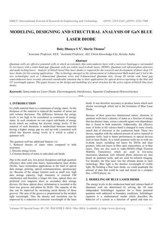
Modeling, designing and structural analysis of ga n blue
1. IJRET: International Journal of Research in Engineering and Technology eISSN: 2319-1163 | pISSN: 2321-7308
__________________________________________________________________________________________
Volume: 03 Special Issue: 01 | NC-WiCOMET-2014 | Mar-2014, Available @ http://www.ijret.org 26
MODELING, DESIGNING AND STRUCTURAL ANALYSIS OF GaN BLUE
LASER DIODE
Baby Dhanya S N1
, Sherin Thomas2
1
Associate Professor, ECE, 2
Assistant Professor, AEI, Christ Knowledge City, Kerala, India
Abstract
Quantum wells are effective potential wells in which an extremely thin semiconductor layer with a narrower band-gap is surrounded
by two layers with a wider band gap. Quantum wells are widely used in diode lasers, HEMTs, Quantum well infrared photo detectors
and mode locking lasers. Analysis of InGaN based blue laser diodes is required for the research and development of future deep UV
laser diodes for bio-sensing applications. This technology emerged as the advancement of 3-dimensional Bulk model and it led to the
new technologies such as 1-dimensional Quantum wires and 0-dimensional Quantum dots. Group III nitride wide band gap
semiconductors have recently attracted considerable attention due to their applications for optical devices operating in the blue and
UV wavelength regions. This paper focuses on the design and modelling of a novel structure for the active region of InGaN blue laser
diodes
Keywords: Semiconductor Laser Diode, Electromagnetic Interference, Separate Confinement Heterostructure
-----------------------------------------------------------------------***-----------------------------------------------------------------------
1. INTRODUCTION
In a bulk material there is a continuum of energy states. As the
thickness of the material is reduced the number of atoms per
unit volume decreases. The difference between the energy
levels is too high to be considered as continuum of energy
states. In such situations we can expect sub-bands of energy
levels which are nothing but discrete energy levels. If the
material of such thickness is sandwiched between materials
having a higher energy gap we end up with a potential well
which has discrete energy levels in it which is called a
quantum well.
The quantum well has additional features viz:
1. Reduced density of states when compared to bulk
structures.
2. Discrete energy levels.
3. Constant density of states in individual sub bands.
Due to the small size, low power dissipation and high quantum
efficiency than solid state lasers, Semiconductor laser diodes
(SLDs) have tremendous applications in the field of optical
data storage, printing, optical communications, spectroscopy
etc. Because of the unique features such as small size, high
data storage capacity, high immunity to external EM
interference and therefore a longer life time, optical discs are
preferred over magnetic discs as secondary data storage
devices. On these optical discs, information is recorded in the
form tiny grooves and planes by SLDs. The capacity of the
disc can be improved by increasing aerial density of these
grooves. The area of the groove is proportional to the incident
light wavelength. Thus the density and resolution can be
improved by a reduction in emission wavelength of the laser
diode. It was therefore necessary to produce lasers which emit
shorter wavelength which led to the formation of Blue Laser
Diode.
Because of their quasi-two dimensional nature, electrons in
quantum wells have a density of states as a function of energy
that has distinct steps, versus a smooth square root dependence
that is found in bulk materials. Additionally, the effective
mass of holes in the valence band is changed to more closely
match that of electrons in the conduction band. These two
factors, together with the reduced amount of active material in
quantum wells, lead to better performance in optical devices
such as laser diodes. As a result quantum wells are in wide use
in diode lasers, including red lasers for DVDs and laser
pointers, infra-red lasers in fibre optic transmitters, or in blue
lasers. They are also used to make HEMTs (High Electron
Mobility Transistors), which are used in low-noise
electronics. Quantum well infrared photo detectors are also
based on quantum wells, and are used for infrared imaging.
For decades, the blue laser was the ultimate dream in laser
technology. Blue light is the shortest wavelength of visible
light. By building a blue laser diode, we could quadruple the
amount of data that could be read and stored on a compact
disc, a DVD player, etc.
2. MODELING OF BLUE LASER DIODE
The energy levels in the conduction band and valence band of
Quantum well are determined by solving the 1D time
independent Schrödinger equation for a finite potential
quantum well subjected to boundary conditions. Schrödinger
equation is a mathematical model which describes the
behavior of a system as a function of spatial and time co-
2. IJRET: International Journal of Research in Engineering and Technology eISSN: 2319-1163 | pISSN: 2321-7308
__________________________________________________________________________________________
Volume: 03 Special Issue: 01 | NC-WiCOMET-2014 | Mar-2014, Available @ http://www.ijret.org 27
ordinates in terms of a wave function Ψ. solving the
Schrödinger equation in time independent form gives the
possible wave functions that can exist within the region.
Different Ψ functions give the possible energy levels in the
region.
Time Independent Schrodinger Equation is given by:
E is the energy of the system.
Carriers at the edge of energy bands follow a parabolic E-k
relationship. They behave as free carriers as observed for
uniform potentials. The carriers encounter no potentials inside
the well. The carriers encounter potential barriers, Vo, at the
extremes of the low band gap semiconductor.
Substituting,
The equation becomes,
This gives
Outside the well, (x) = 0 and (x) = A sinkx. Putting x = a,
where a is the thickness of quantum well, gives
Thus the equation becomes,
This equation gives the energy levels in a quantum well. The
energy levels for different values of n can be plotted as shown
below:
Fig- 1 Energy levels in quantum well
The wave functions can be plotted by giving,
which gives the equation,
Blue laser diodes emit light in the wavelength of range
440nm- 485nm. This region of operation has led to
applications in optical data storage i.e. in CDs and DVDs and
high resolution printing. Emission of photons in the blue
region requires a material having a band gap of 2.64ev.
Fig -2 Wave functions in quantum well
3. DESIGNING OF BLUE LASER DIODE
This band gap can also be tailored by alloying wide band gap
(>2.4ev) materials. The materials under investigation were
group III-V, II-V1, and SiC investigation as they possessed
sufficient energy gap for emission in the blue region.
Experimental results showed that laser diodes fabricated using
GaN had high internal quantum efficiency and longer life time
inspite of having a high dislocation density. These results led
to the commercialization of GaN based blue laser diodes. Thus
InGaN is used as the active region and AlGaN as the cladding
region. For the effective electrical confinement of optical field
in SCH structure, the refractive index difference between core
3. IJRET: International Journal of Research in Engineering and Technology eISSN: 2319-1163 | pISSN: 2321-7308
__________________________________________________________________________________________
Volume: 03 Special Issue: 01 | NC-WiCOMET-2014 | Mar-2014, Available @ http://www.ijret.org 28
and cladding must be very high. The proposed structure is
shown below:
Fig- 3 Proposed structure
Laser diodes with different design layout have been fabricated
and most of the designs reported were SCH devices which had
multiple quantum wells as the active region with GaN as the
optical guiding region and AlGaN layer as the cladding region
.Additionally there is an electron blocking p-AlGaN layer
which prevented overflow of electrons. Laser diodes with
different emission wavelengths, efficiencies, output powers
and threshold currents were reported by varying the properties
of each of these layers. The active region consisting of InGaN
quantum wells is responsible for confining the carriers. The
proposed model is an SCH structure with InGaN MQW as the
active region, GaN as optical guiding region and AlGaN as the
cladding region for emission wavelength in the range of
440nm – 485nm. Multiple quantum wells are used to increase
the amount of power emitted by the laser diode as the power
generated by a single quantum well is limited by the saturation
effects.
4. STRUCTURAL ANALYSIS OF BLUE LASER
DIODE
When the InGaN quantum well is of thickness comparable to
the scattering length of the carriers the carriers do not
thermalize sufficiently to settle down at lower energy states. In
order to increase the fraction of carriers settling down at lower
energy states a higher carrier density is needed. This implies
an increase in the threshold current density of the laser diode.
Multiple quantum wells solve this problem to some extent.
Coupling of a quantum via a thin barrier to another barrier
increases the effective length of the active region. To get a
uniform distribution of carriers in the quantum wells if the
effective mass of the electrons in the quantum wells close to
the n – side is increased and the effective mass of holes in the
quantum wells is reduced then we can have a uniformity in the
distribution of carriers across the active region. If uniformity
is achieved the AlGaN blocking layer responsible for
preventing the carriers from overflowing can be removed. The
problem with AlGaN blocking layer is that it prevents the
overflow of carriers(electrons) at the cost of increased series
resistance and also presents a barrier to the free flow of holes
into the quantum well from the p-region. A double barrier
quantum well formed by placing a wider quantum well above
a narrow quantum well can reduce the carrier overflow and
thereby causes a reduction in the threshold current density of
the laser diode. A 1D – photonic crystal is composed of
alternating stacks of layers having a low and high index of
refraction. These structures reflect light at any polarizations,
any incidence angle and over a wide range of wavelengths.
The emission in a quantum well is dominated by the
difference in energy levels between the lowest discrete energy
level in the conduction band and the highest discrete energy
level in the valence band. The discrete energy levels in the
conduction and valence band are given are given by solving
the Schrödinger time independent wave equation for both the
potential wells in the conduction band and valence band
respectively. As most of the carriers settle down into the
lowest energy level the emission energy is dominated by lower
energy levels. The emission wavelength is dependent on the
position of the energy levels relative to the band edge.
5. SIMULATION OF QUANTUM WELL IN BLUE
LASER DIODE
The wave functions and energy levels of InGaN quantum well
of thickness 60 micrometers have been simulated using
Matlab. The output is obtained by solving 1D Schrodinger
equation for a finite potential well. The quantum well
thickness in micrometer unit is taken along x-axis. Along y-
axis two parameters are taken: the energy of quantum well in
eV unit and the wavefunction. The equation for energy has
been obtained as:
From the equation, it is clear that E depends only on the no. of
energy levels as all the other parameters are constant. Thus for
different values of n=1,2,3 and 4, different energy levels has
been plotted.
Also the equation for wave function gas been obtained as:
Here also, the wave functions depend only on the value of n as
all other parameters are constant. Hence wave functions have
been plotted for values of n=1,2,3 and 4. The graph obtained
using matlab is shown below:
4. IJRET: International Journal of Research in Engineering and Technology eISSN: 2319-1163 | pISSN: 2321-7308
__________________________________________________________________________________________
Volume: 03 Special Issue: 01 | NC-WiCOMET-2014 | Mar-2014, Available @ http://www.ijret.org 29
Fig - 4 Energy level and Wave functions in InGaN quantum
well simulated using Matlab
A p-n junction semiconductor laser diode has the disadvantage
of improper optical confinement, leading to heavy losses. So a
large current was required for the lasing action. A Double
Heterostructure Laser Diode (DHLD) formed by sandwiching
a lower band gap material in between two higher band gap
materials was a solution to this problem to an extent. When
forward biased, the injected carriers were trapped in the
potential well formed by the structure, thereby preventing the
loss of carriers. As the thickness of this potential well
decreased, the lasing action was found to be obtained at lower
threshold current densities which was the formation of
quantum well laser diode. Thus the blue laser diode was
obtained.
6. CONCLUSIONS
Designs for the active region have been proposed to achieve
uniform distribution of carriers across the active region of the
quantum well to achieve lasing at low energies at a threshold
current density compared to the conventional laser diode
structures. These designs can also be applied to InGaN LEDs
to prevent the overflow of carriers in the proposed quantum
well laser diode structures. These results can be applied
towards research and development of AlInGaN deep UV laser
diodes. As for the future work, InGaN laser diodes based on
the proposed structure have to be grown and tested. The
parameters like quantum well thickness, barrier thickness have
to be varied to get the lowest threshold current density for the
laser diode that is the optimum laser diode design.
REFERENCES
[1]. Ben G. Streetman, Sanjay Kumar Banerjee, "Solid State
electronic devices" ,Pearson Education Inc., 2008
[2]. Bahaa E. A. Saleh,"Fundamentals of Photonics", John
Wiley and Sons,Inc 1991.
[3]. Larry A Coldren, Scott W.Corzine, "Diode Lasers and
Photonic", Wiley and Sons,Inc 1995.
[4]. Nick Holonyak Jr, Robert M Kolbas, Daniel Dapkus,
IEEE Journal of Quantum Electronics, VOl,QE-16,No
2,February 1980.
[5]. John T. Torvik, Jacques I. Pankove, Bart J. Van
Zeghbroeck, IEEE Transactions on Electron Devices, 46 (7),
1999.
[6]. K. Wilmers, T. Wethkamp,N. Esser,C. Cobet,W.
Richter,V. Wagner,H. Lugauer,F. Fischer,T. Gerhard M.
Keim,and M. Cardona, Journal of Elec.Materials, Vol. 28,
No.6, 1999.
[7]. Akito Kuramata, Shin-ichi Kubota, Reiko Soejima, Kay
Domen, Kazuhiko Horino, Peter Hacke and Toshiyuki
Tanahashi, Jpn. Journal of Applied Physics,
Vol.38(1999)L481- L483 Part 2, No. 5A, 1 May 1999.
[8]. S. Nakamura, M. Senoh, S. Nagahama, N. Iwasa,
T.Yamada, T.Matsushita, H. Kiyoku, Y Sugimoto, Jap.Journal
of Applied Physics 35(1B), L74 (1996).
[9]. R.B. ADLER, A.C.Smith and R.L Longini, “Introduction
to semiconductor physics”, SEEC Series, vol.1, John Wiley,
New York, 1964
BIOGRAPHIES
BABY Dhanya S.N currently working as
Asso.Prof. in Christ Knowledge
city,Mannoor.She has completed M.Tech in
communication systems from SRM
Engg.college Chennai in 2006.Her interested
areas are wireless
communication&Cryptography.
Sherin Thomas currently working as Assistant
Professor in Christ Knowledge city, Mannoor.
She has completed M.Tech in VLSI&ES from
St.Joseph’s College of Engineering &
Technology Palai in 2014. Her interested areas
are VLSI signal processing & Low power VLSI.