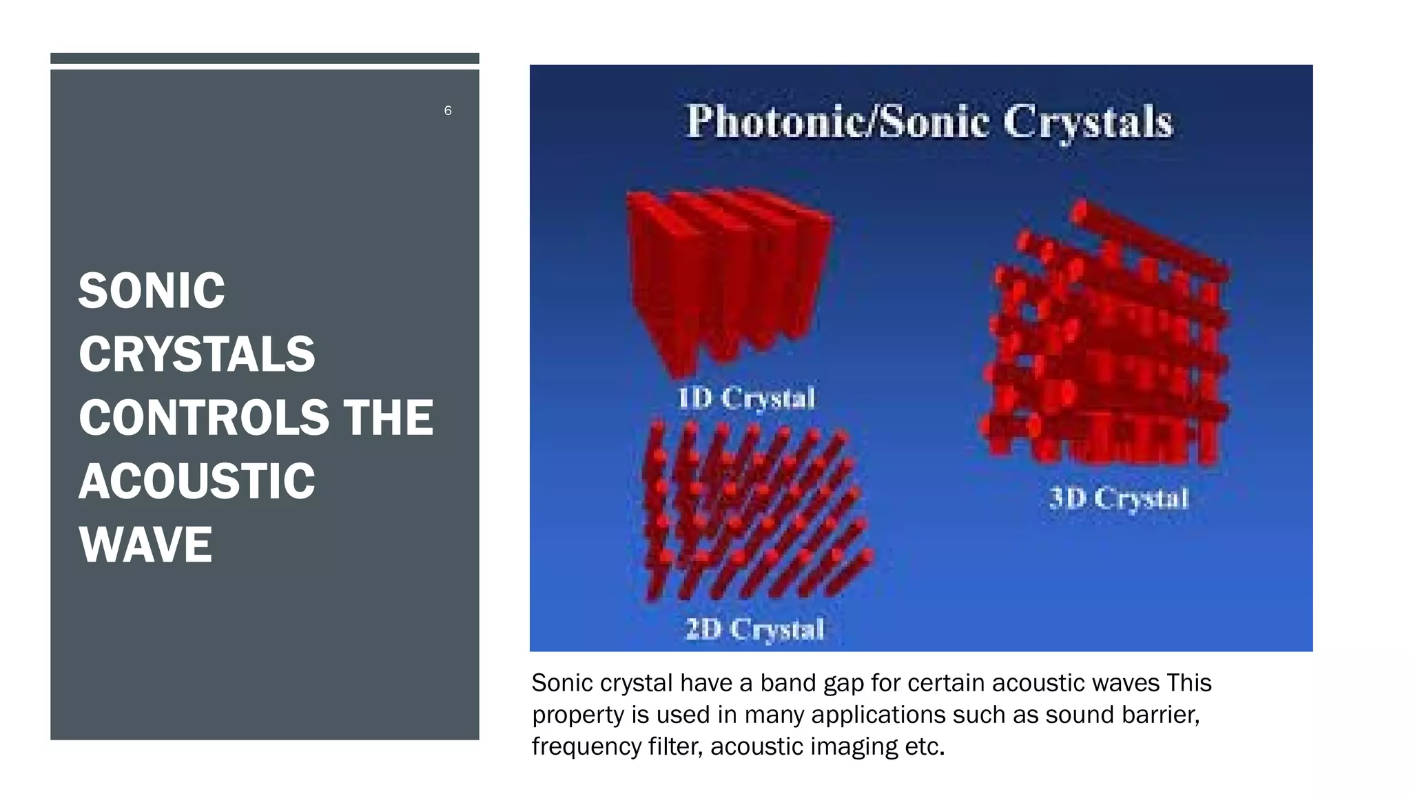
Photonic band gap (PBG) materials are artificially created materials that prevent the propagation of electromagnetic waves within a forbidden bandgap. PBG materials find various applications including EMI shielding, miniaturization of photonic devices, and magnetic field sensing. Photonic crystal fibers use the bandgap effect to guide light and have uses in telecommunications, sensing, and medicine.


![REFERENCES
[1] E. Yablonovitch J. Opt. Soc. Am. B/Vol. 10, No. 2/February 1993
[2] Biswas R., Chan C.T., Sigalas M., Soukous's C.M., Ho K.M. (1996) Photonic Band Gap Materials. In: Soukoulis C.M. (eds) Photonic Band
Gap Materials. NATO ASI Series (Series E: Applied Sciences), vol 315. Springer, Dordrecht. https://doi.org/10.1007/978-94-009-1665-4_
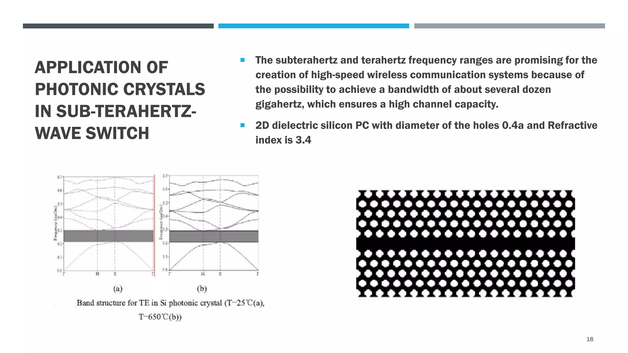
[3] Li Jiusheng l'2, Du Tieying 2,” Application of Photonic Crystals in sub-terahertz-wave Switch”
[4] Xiaoqiuyan Zhang, Min Hu, Sen Gong, Zhenhua Wu, Yueheng Cao, Pengfei Hu and Shenggang Liu “
Theoretical Calculation and Electromagnetic Simulation of Smith-Purcell in Photonic Crystals,2018.
[5] Hong Wu1 * and Feng Li2,3 “ Negative-refraction Effect for Both TE and TM Polarizations in Two-dimensional Annular Photonic Crystals
“2018.
[6] Dr. Gary L. Bastin, ASRC Aerospace “2007 Space and Missile Défense Conference, Huntsville, AL. 13-16 August 2007
[7] Philip St.J. Russell volume “ Photonic crystal fiber” 24.Issue 12.pp 4729-4749,2006
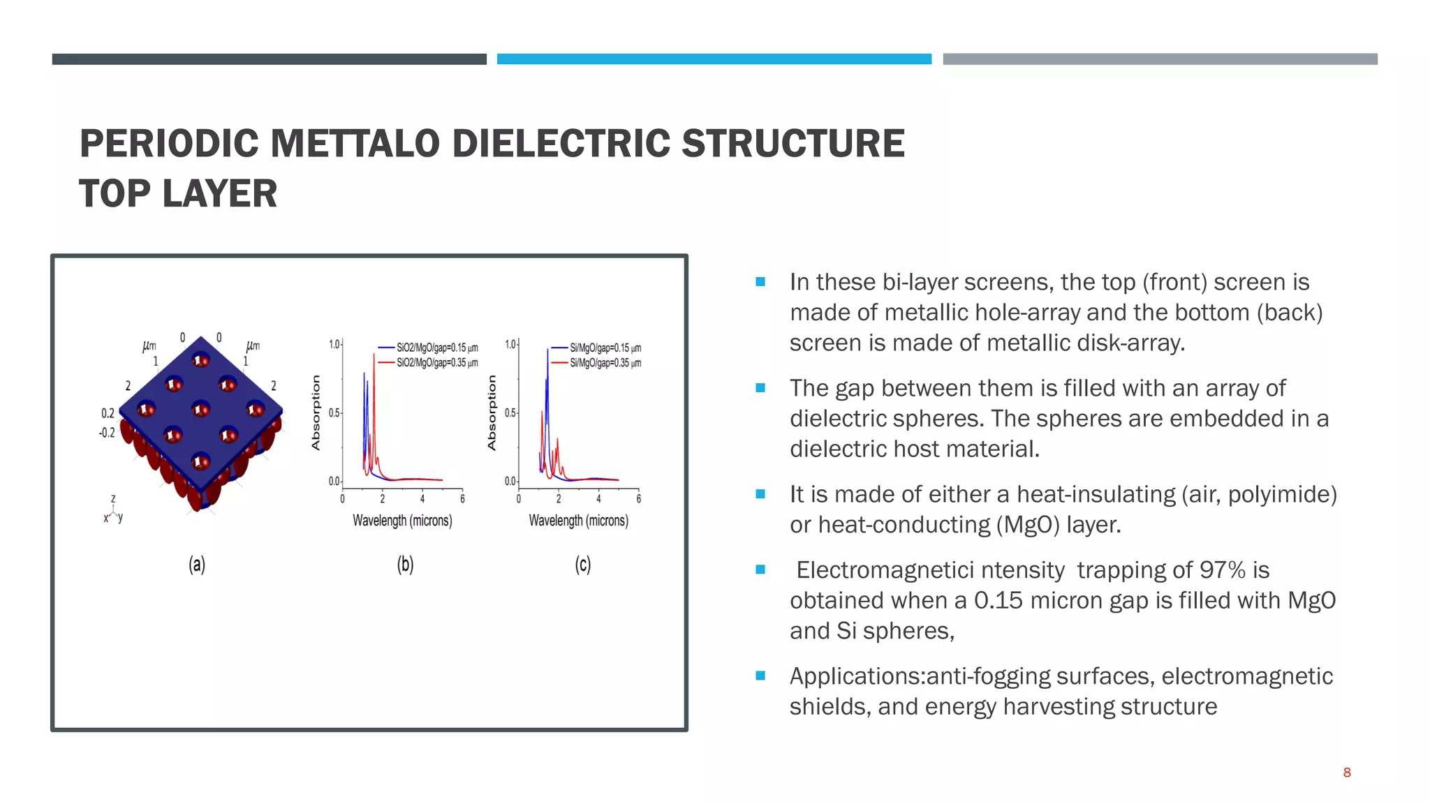
[8] Jean Paul Walker 1 , Venkataraman Swaminathan 2,† , Aisha S. Haynes 2 and Haim Grebel 1,* Periodic Metallo-Dielectric Structures:
Electromagnetic Absorption and its Related Developed Temperatures, 2019
[9] Li Jiusheng, Du Tieying, “ Application of Photonic crystal in sub terahertz range” IEEE 2007 International Symposium on Microwave,
Antenna, Propagation, and EMC Technologies For Wireless Communications.
[10] Ran Gao, Yi Jiang, and Gang Li” A Sandwich Structure for the Magnetic Field Detection With Supe rmodes Interference” EEE
PHOTONICS TECHNOLOGY LETTERS, VOL. 27, NO. 5, MARCH 1, 2015
23](https://image.slidesharecdn.com/pbgatalfdp-220103011038/75/Pbg-atal-fdp-23-2048.jpg)


![[ vol. 10.1142_8179] Andreone, Antonello_ Cusano, Andrea_ Cutolo, Antonello_ ...](https://cdn.slidesharecdn.com/ss_thumbnails/vol-220909082416-3037aa7a-thumbnail.jpg?width=640&height=640&fit=bounds)


