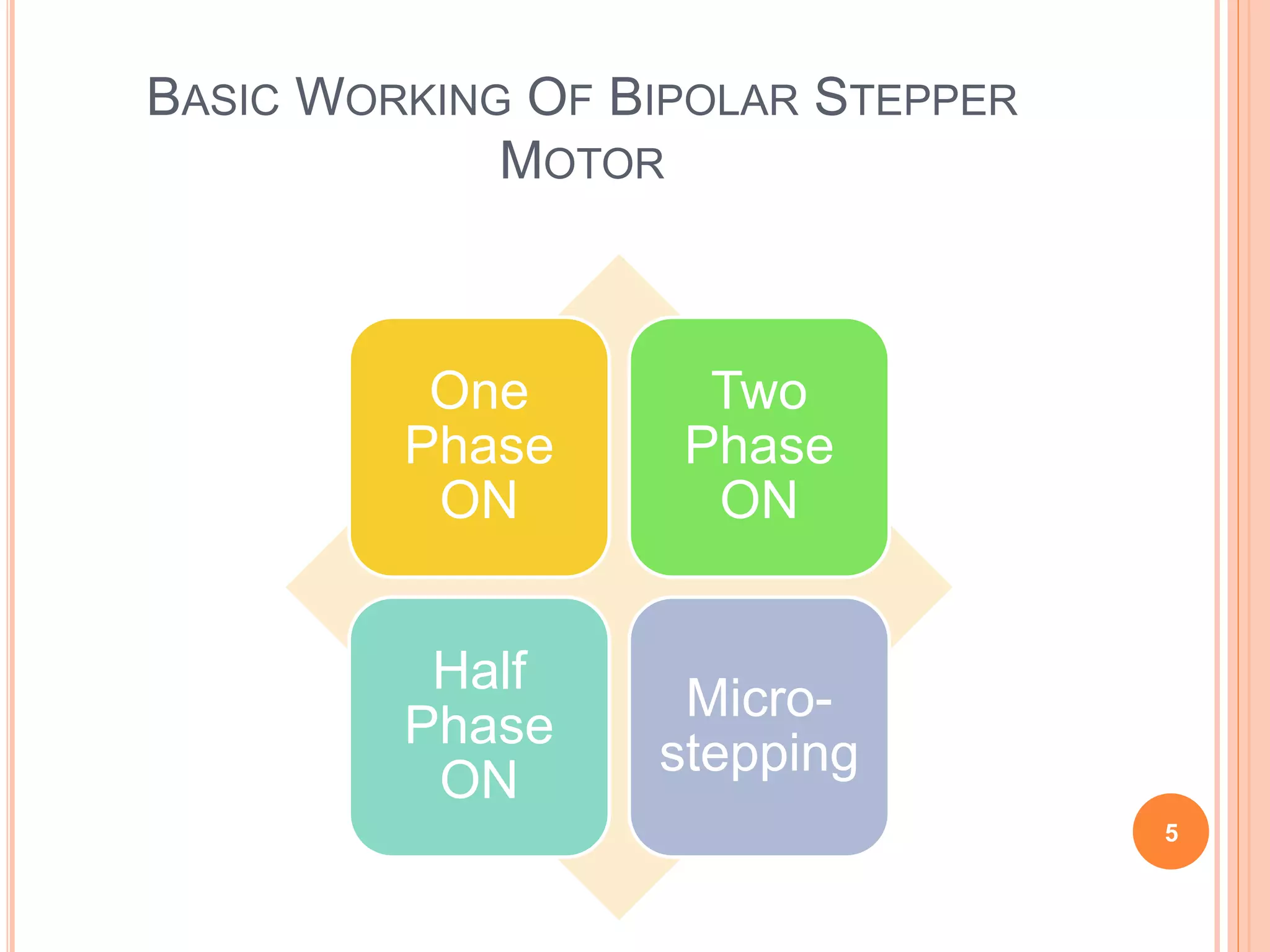
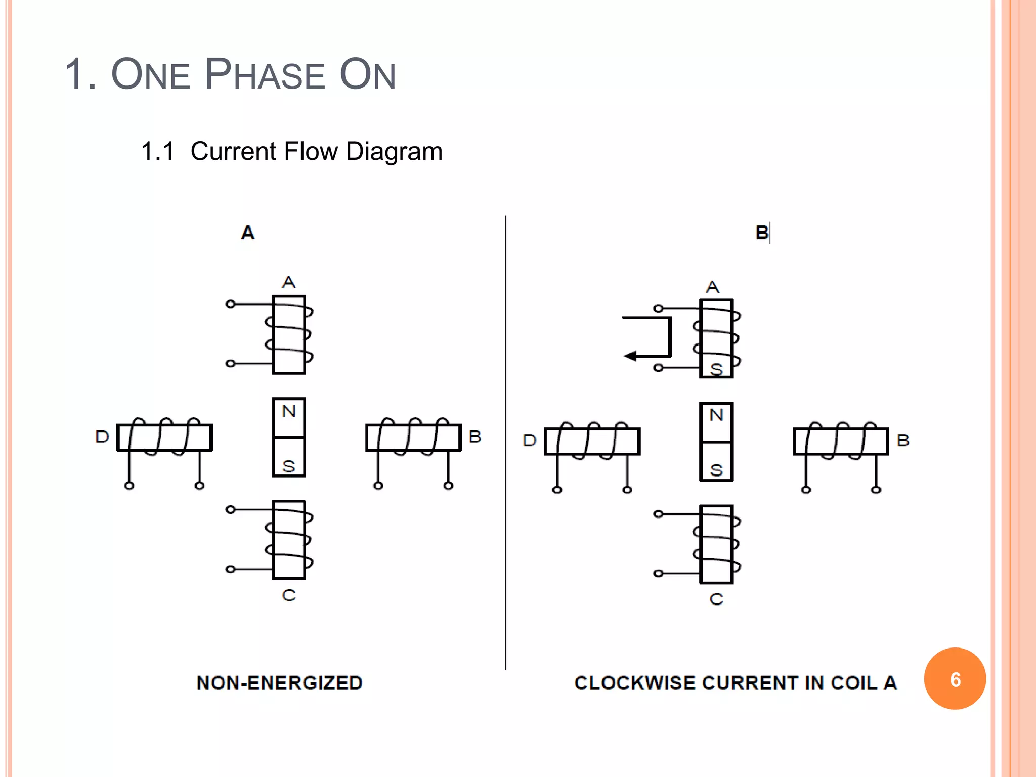
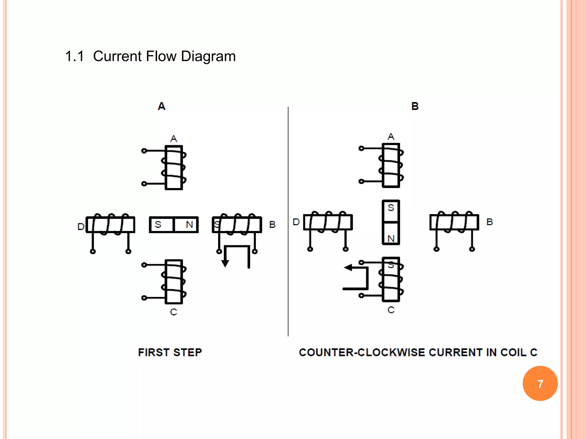
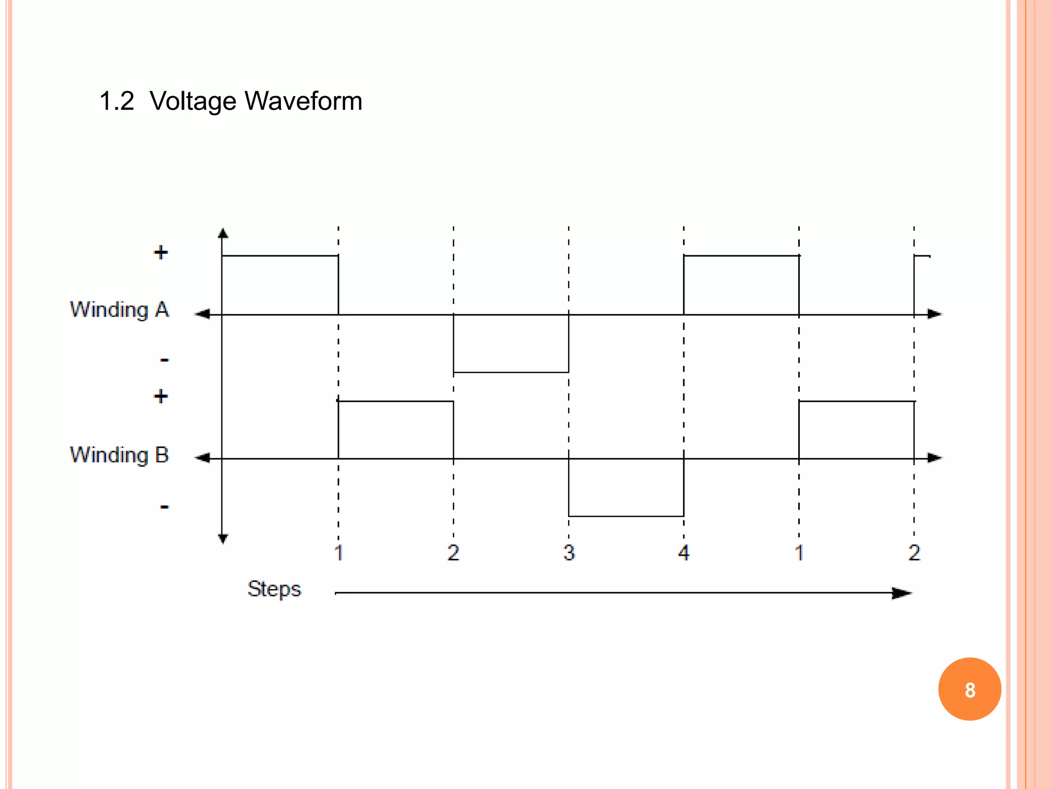
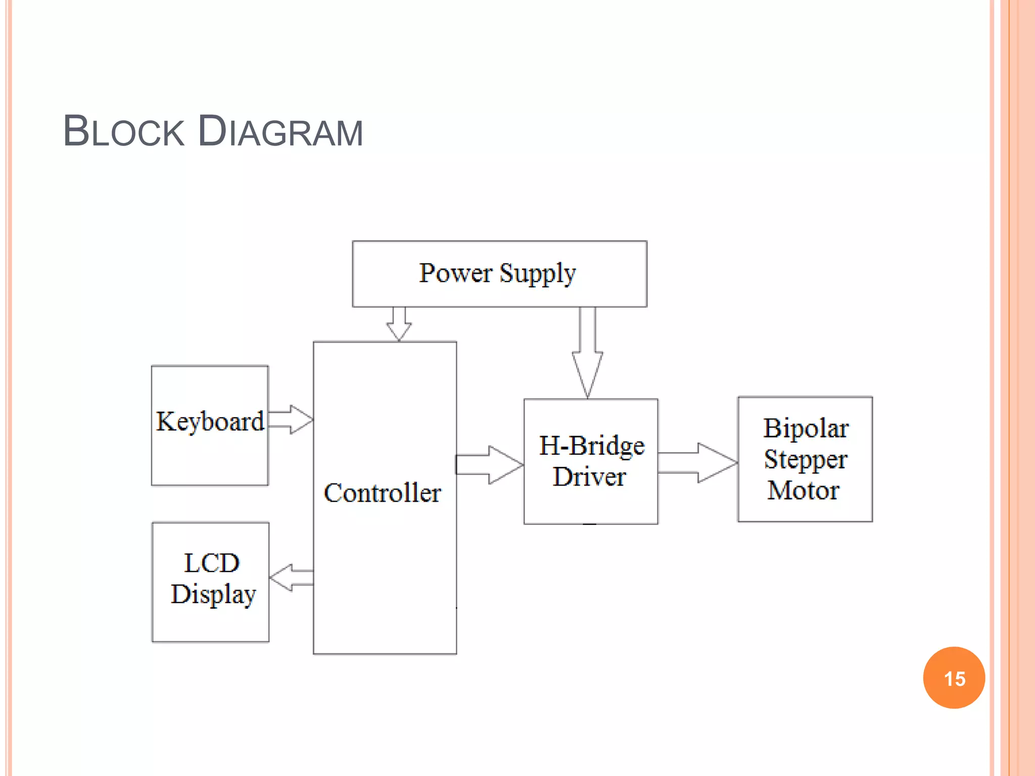
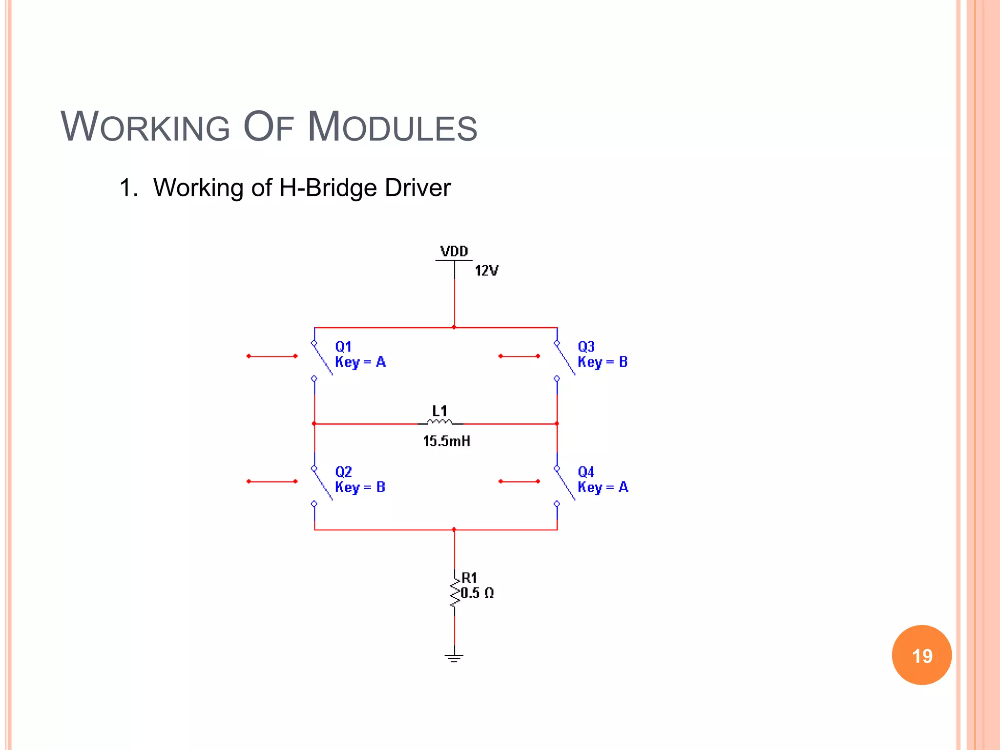
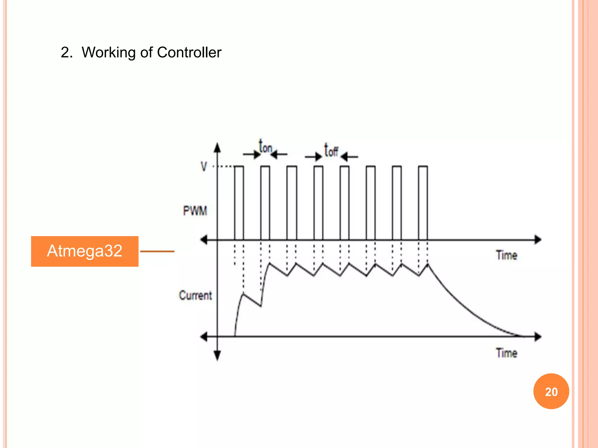
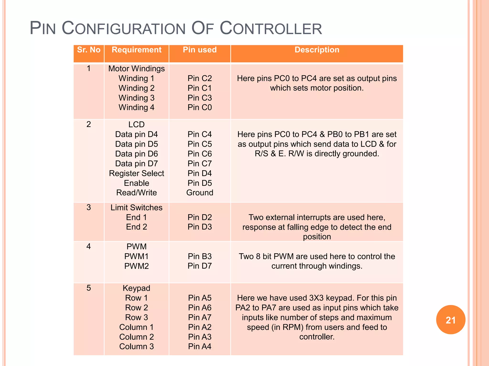
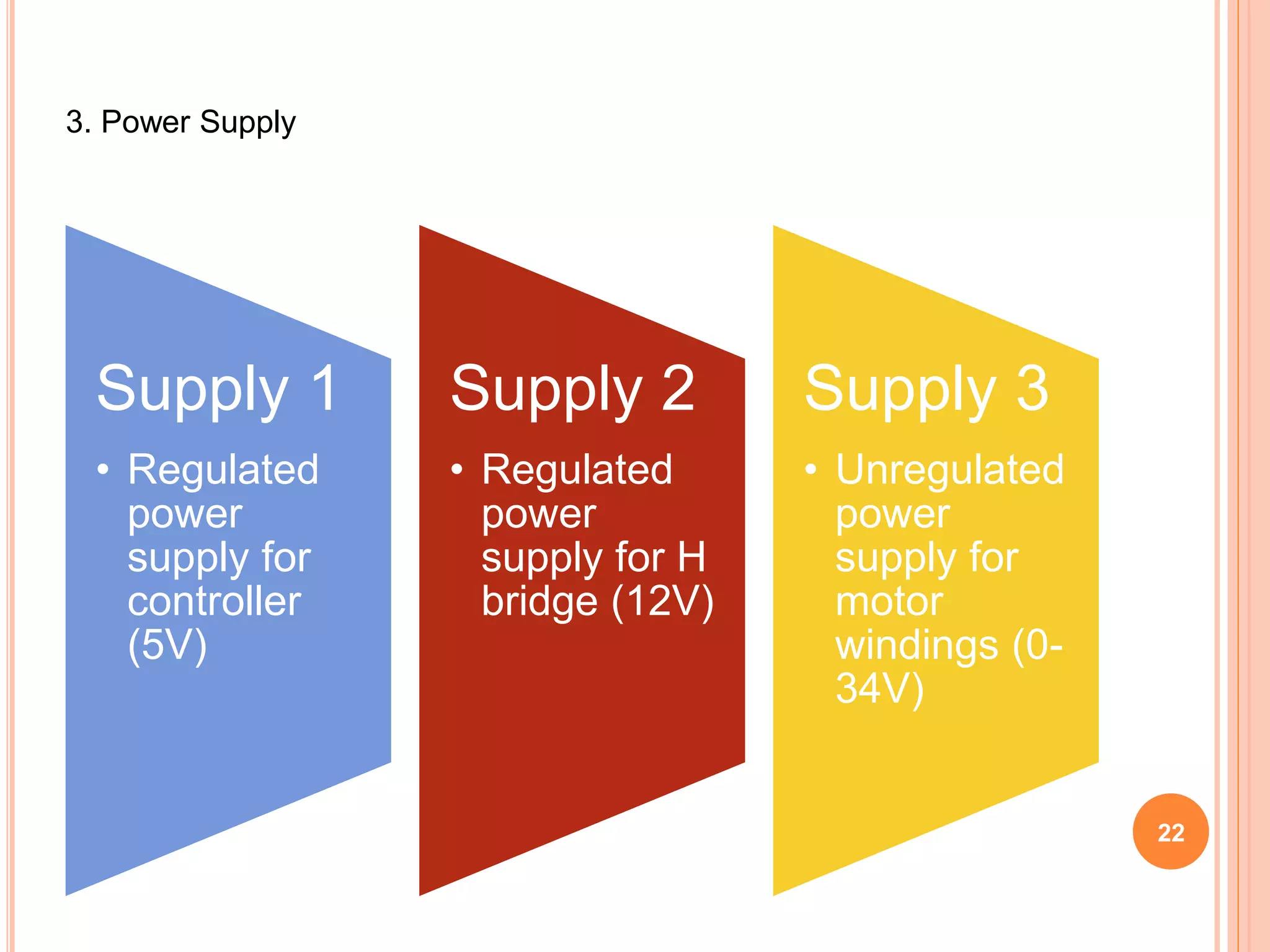
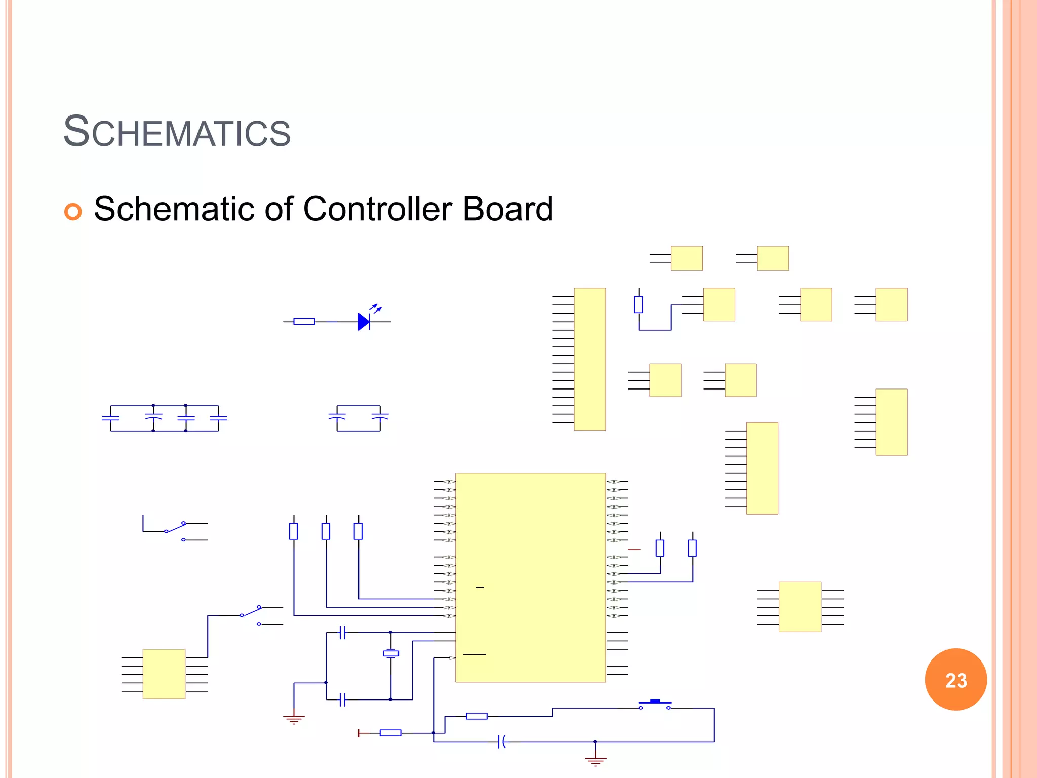
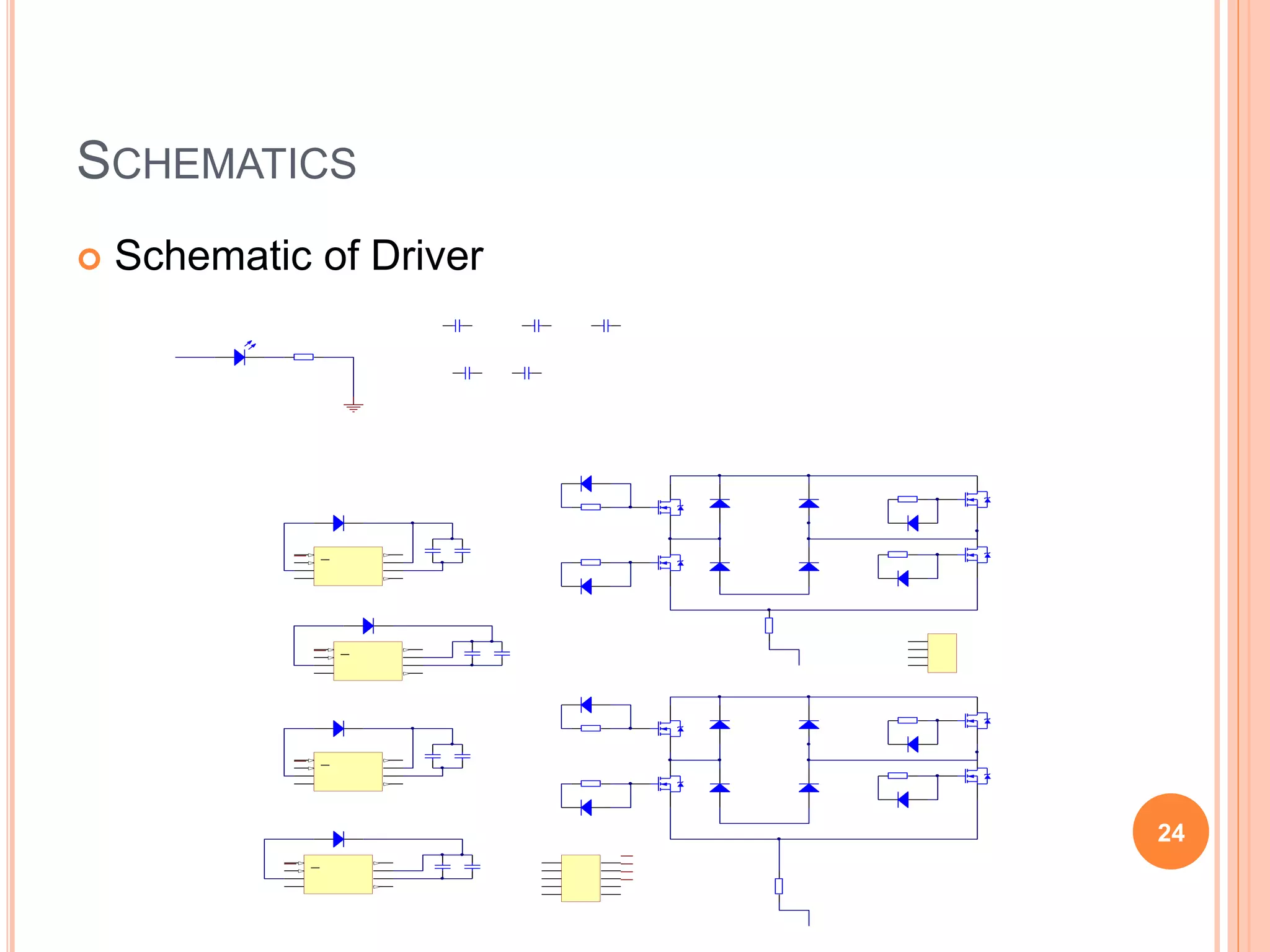
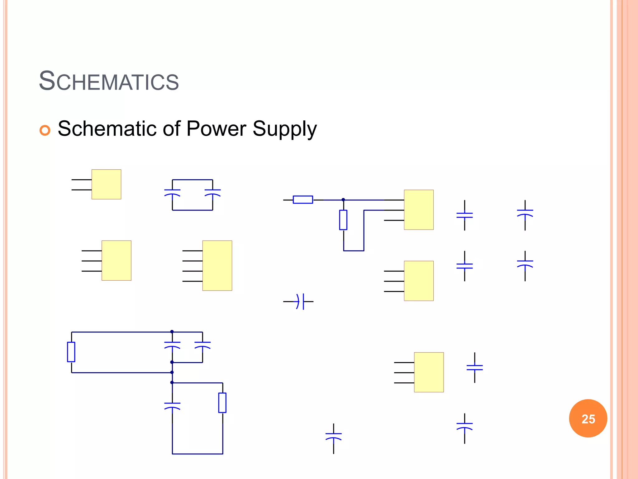
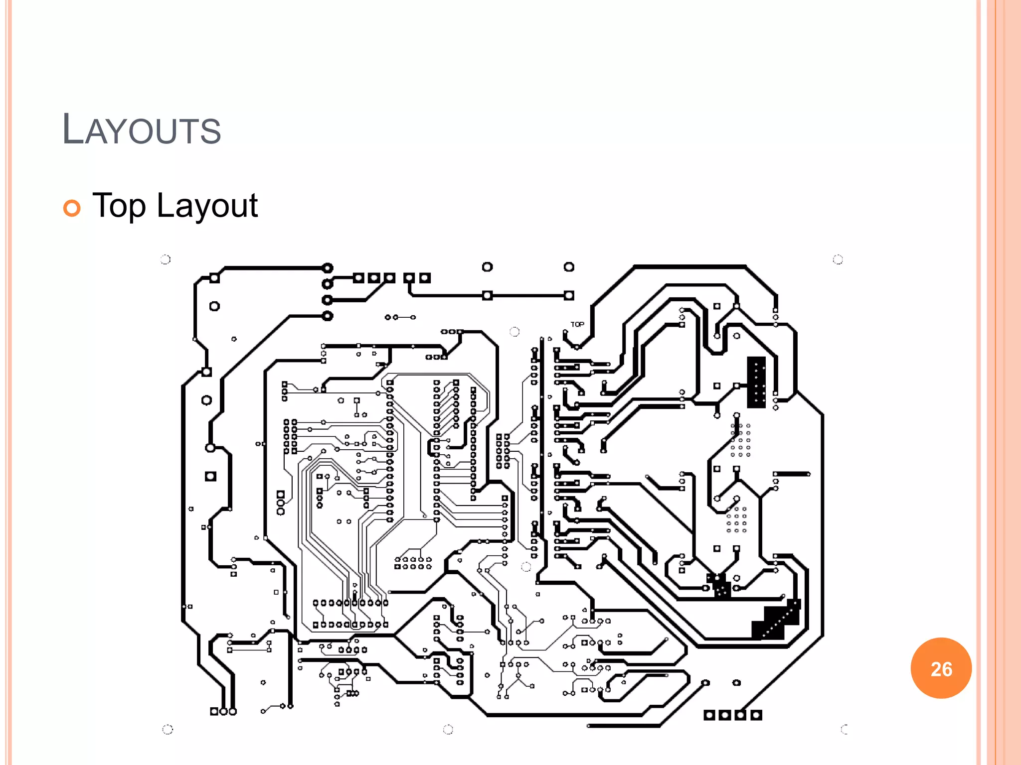
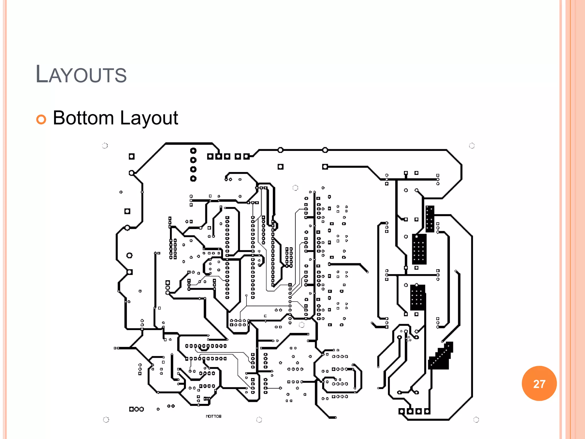
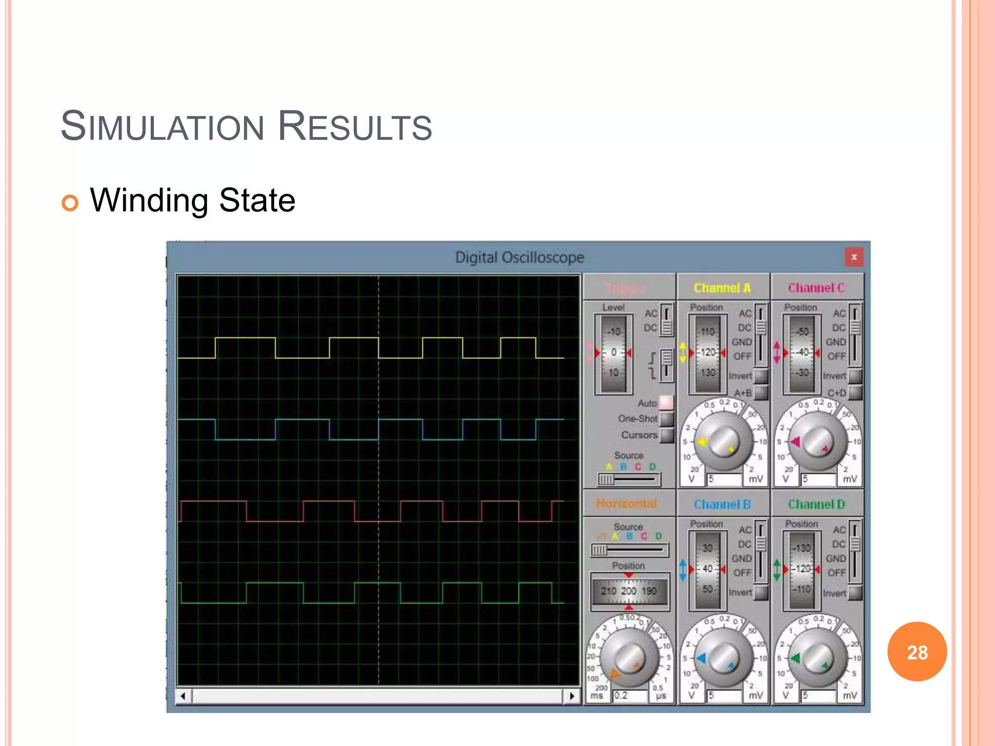
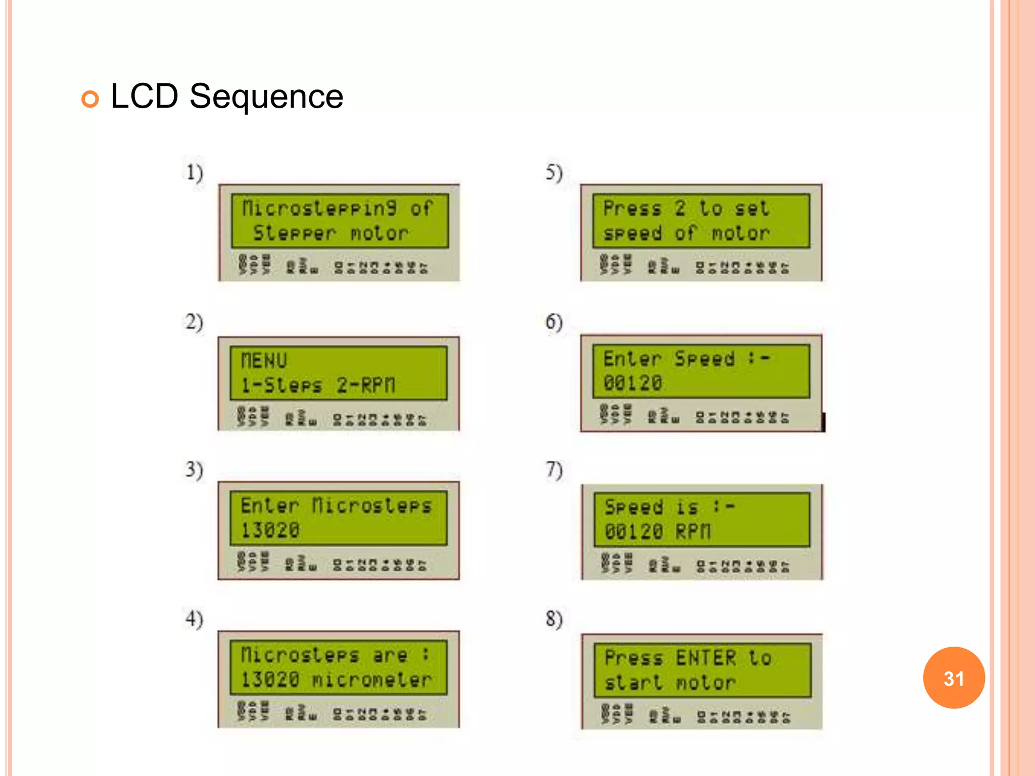
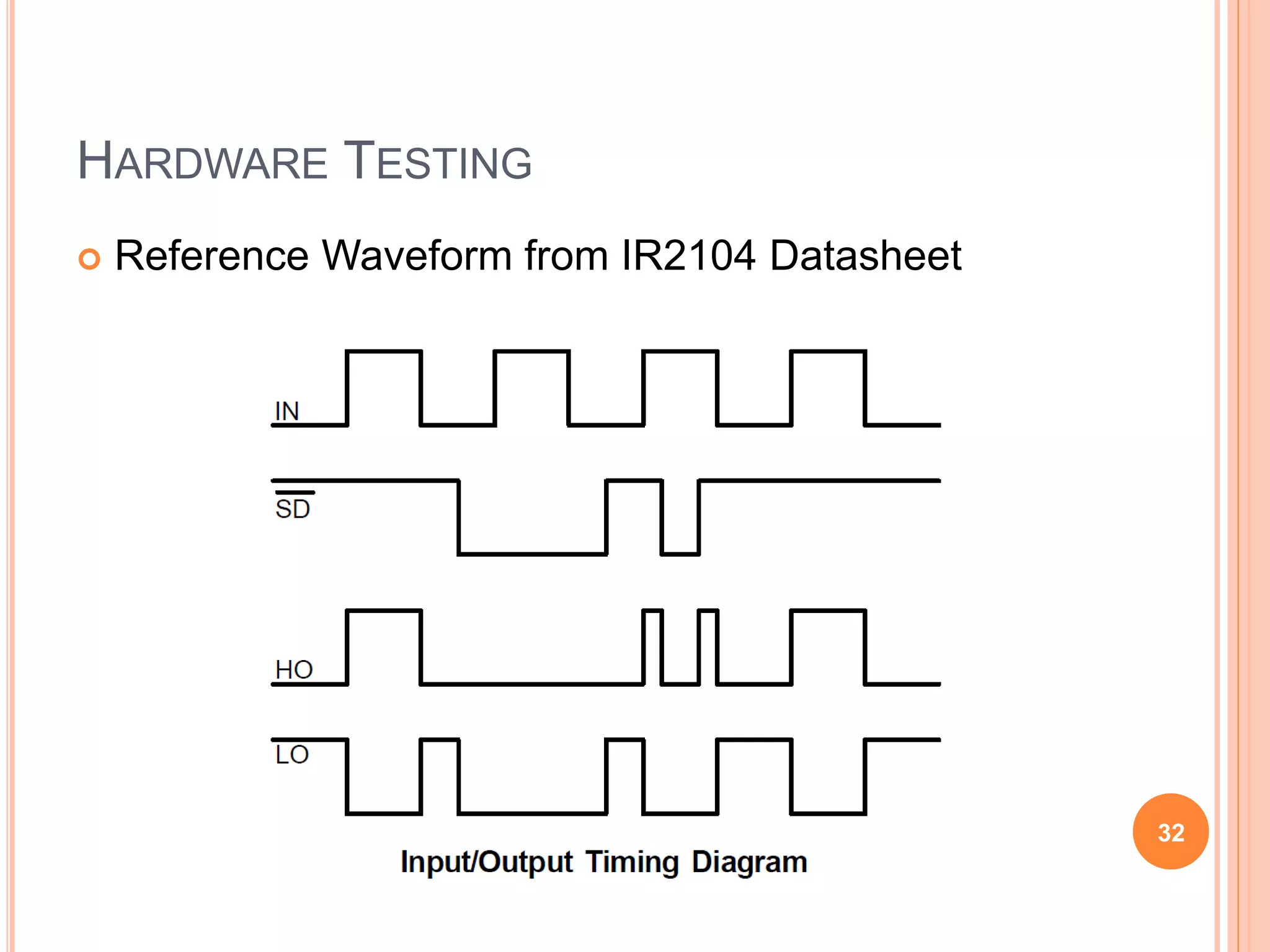
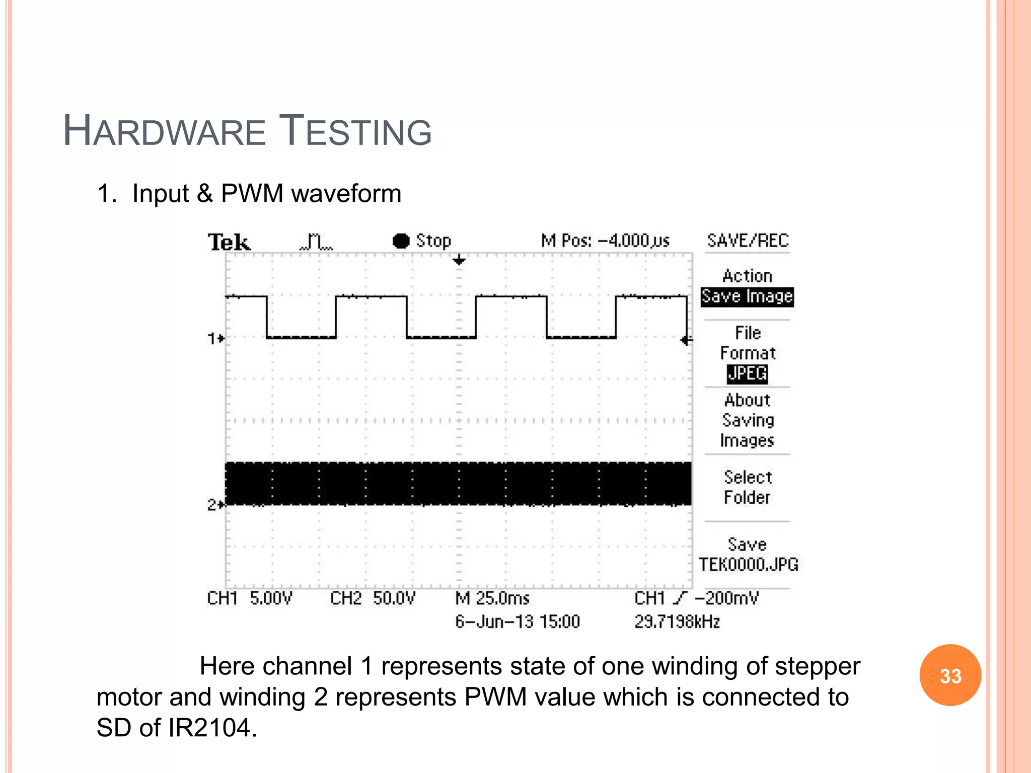
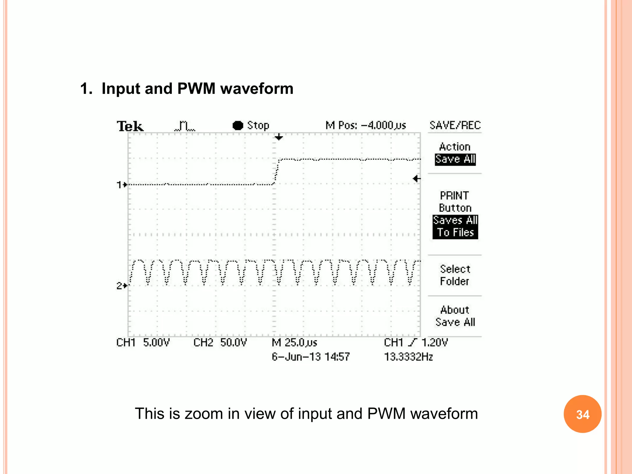
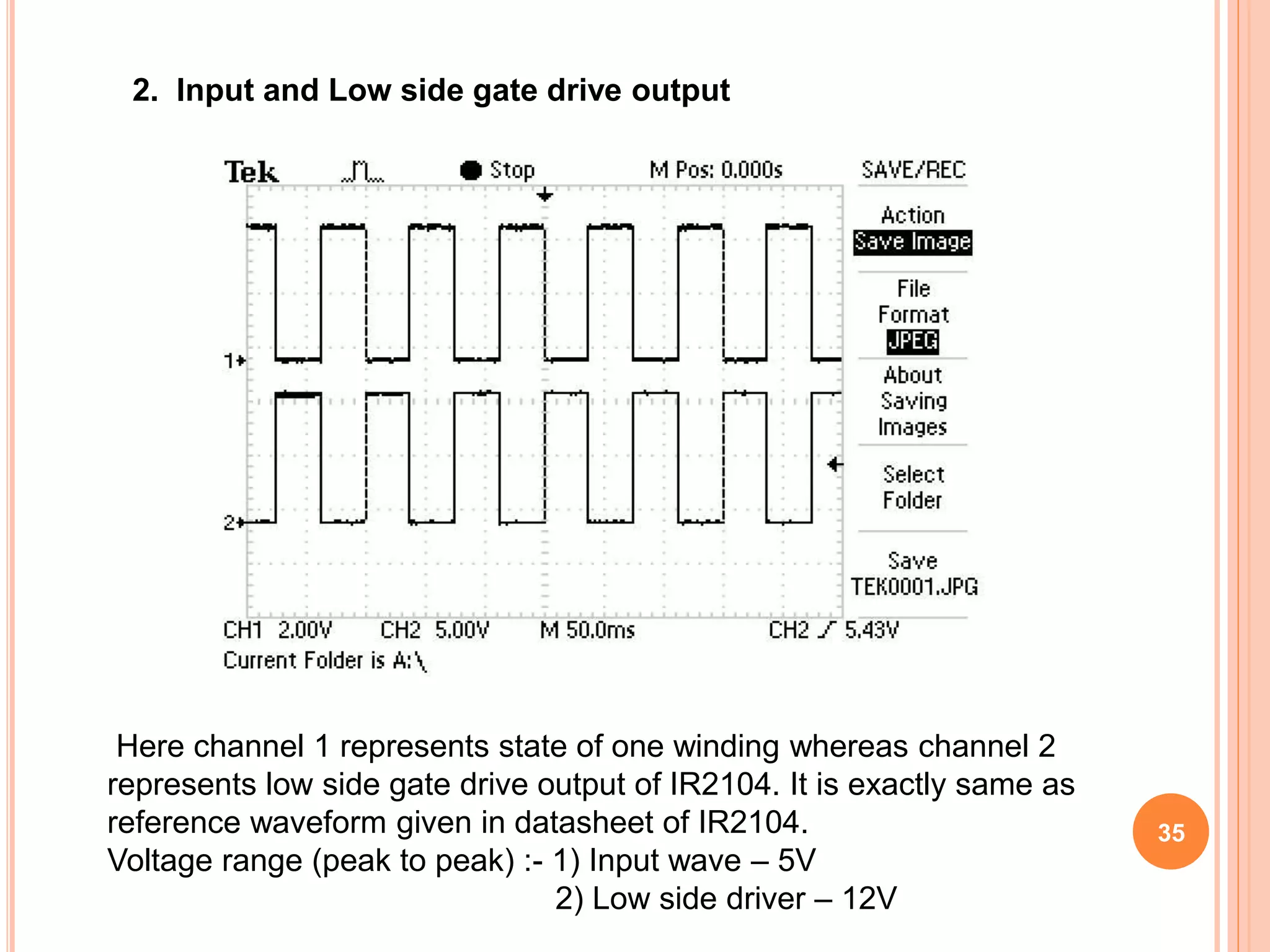
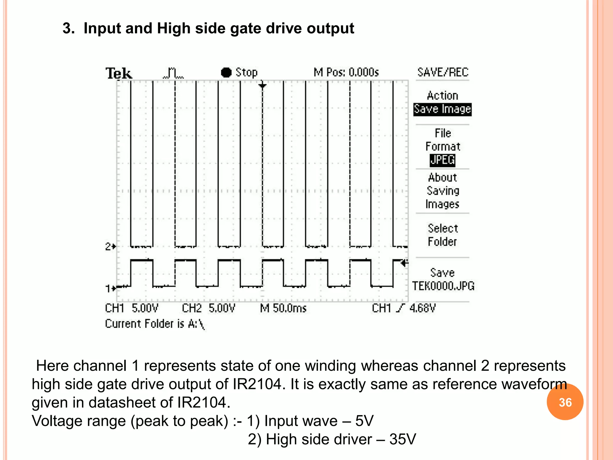
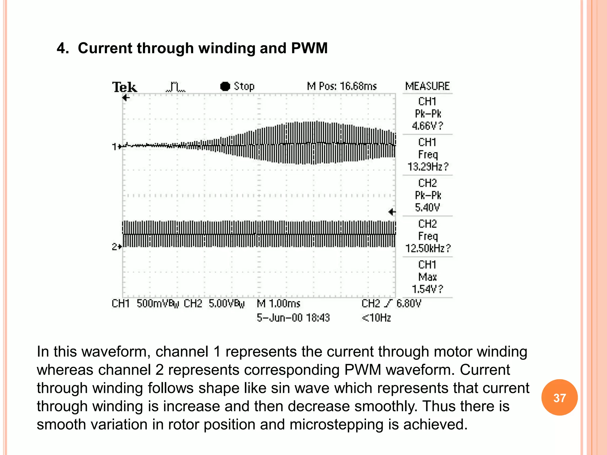
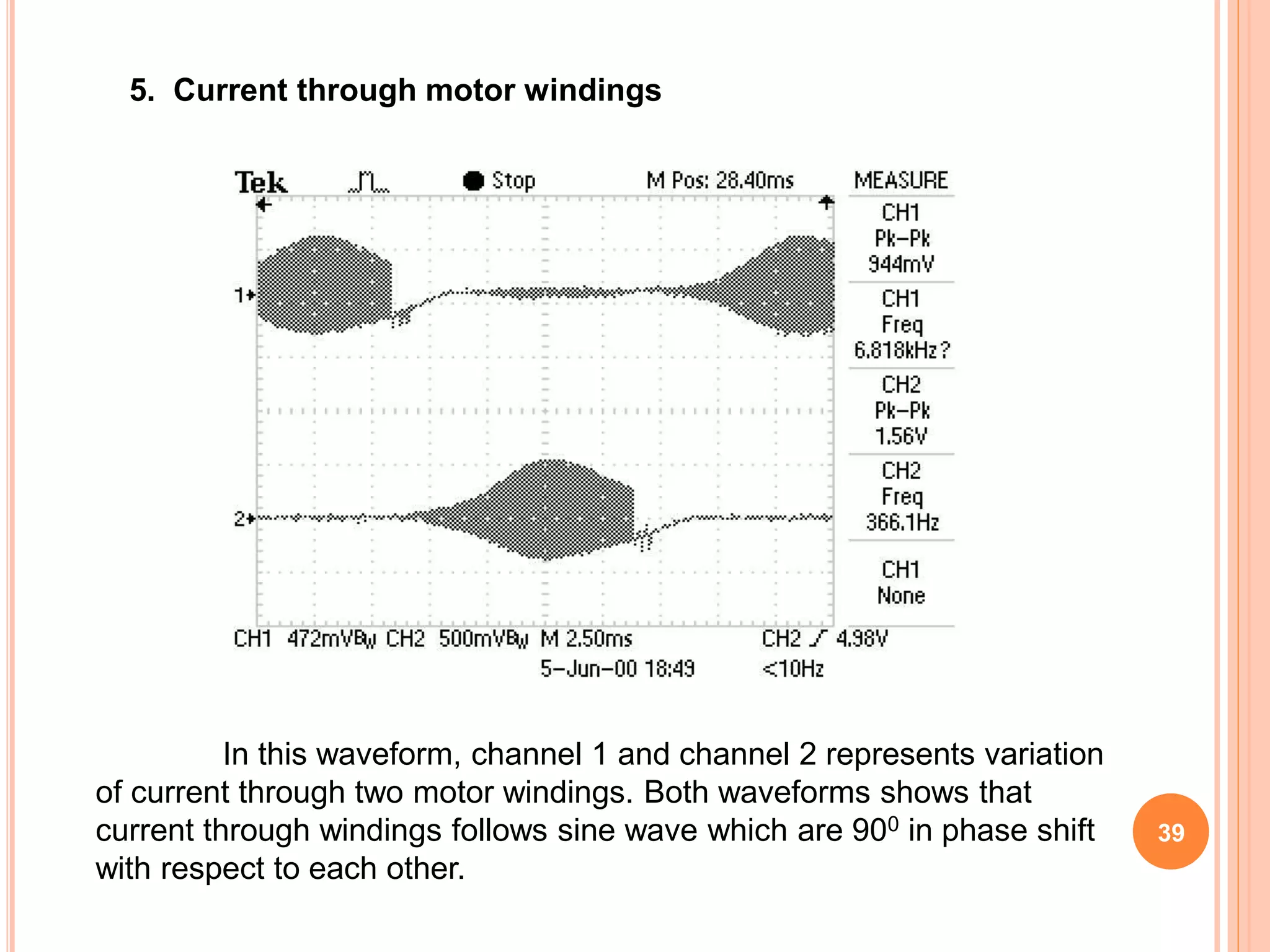
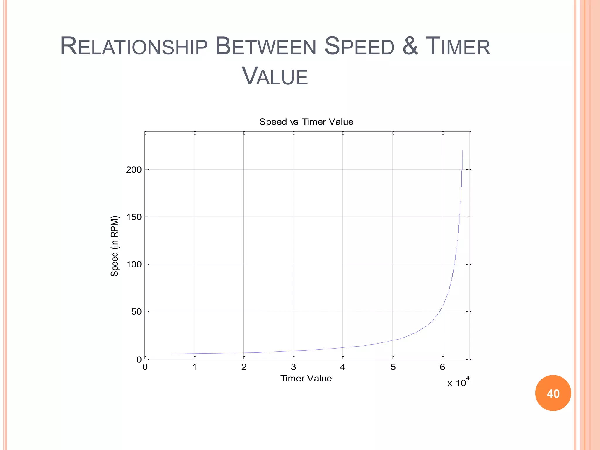
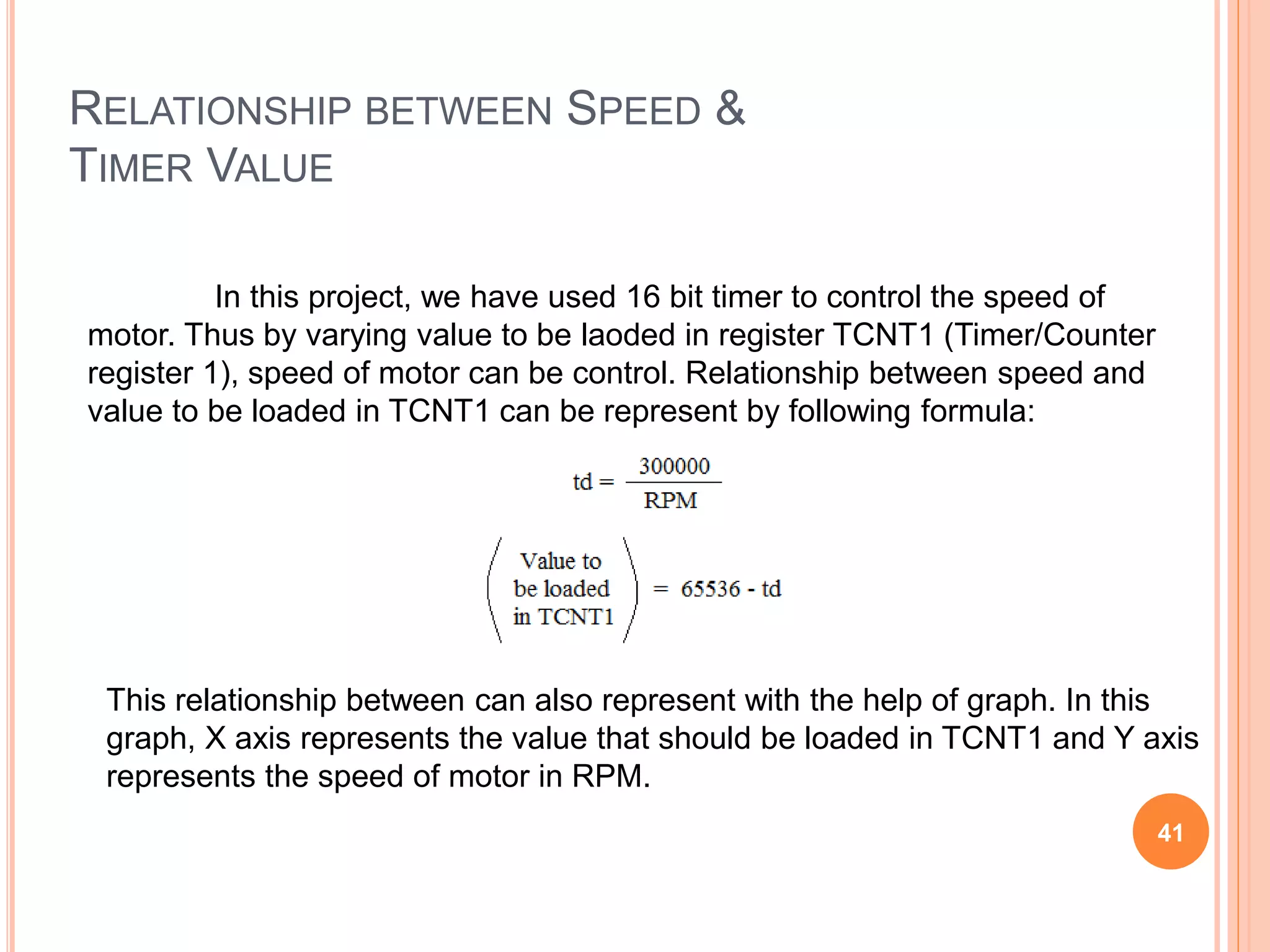
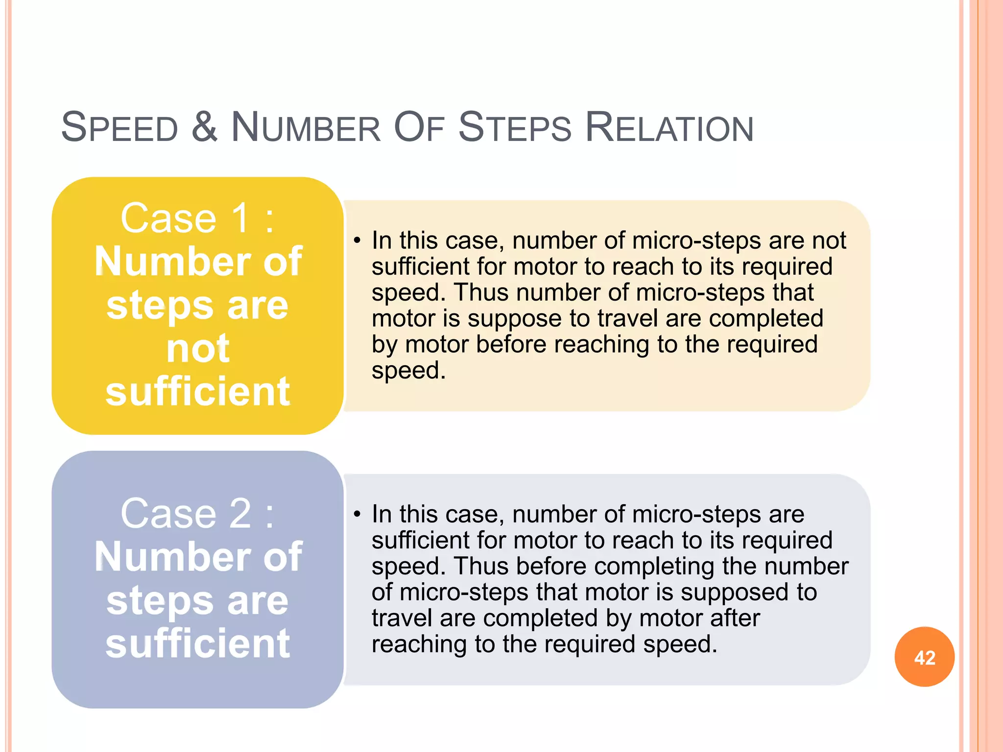
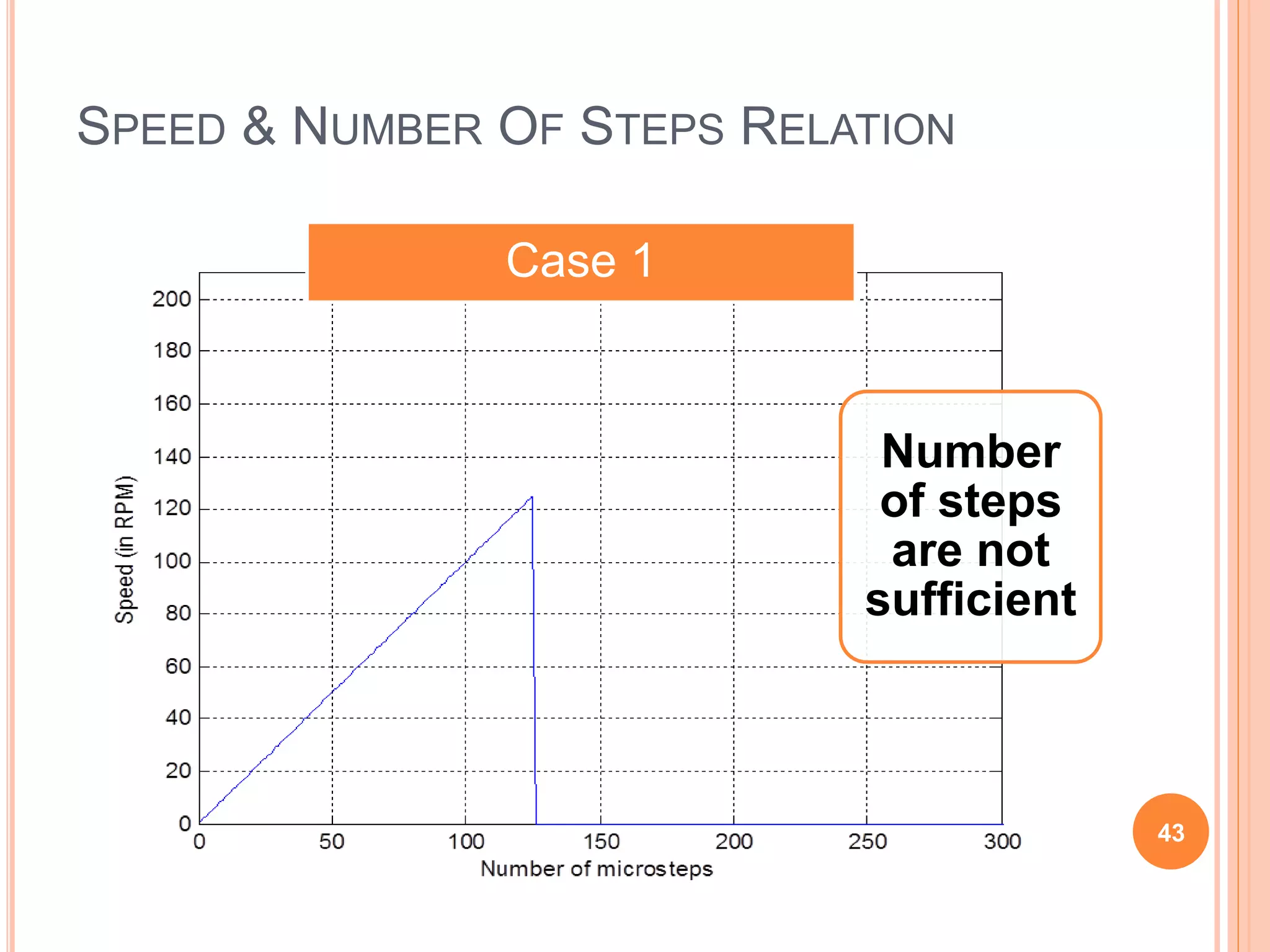
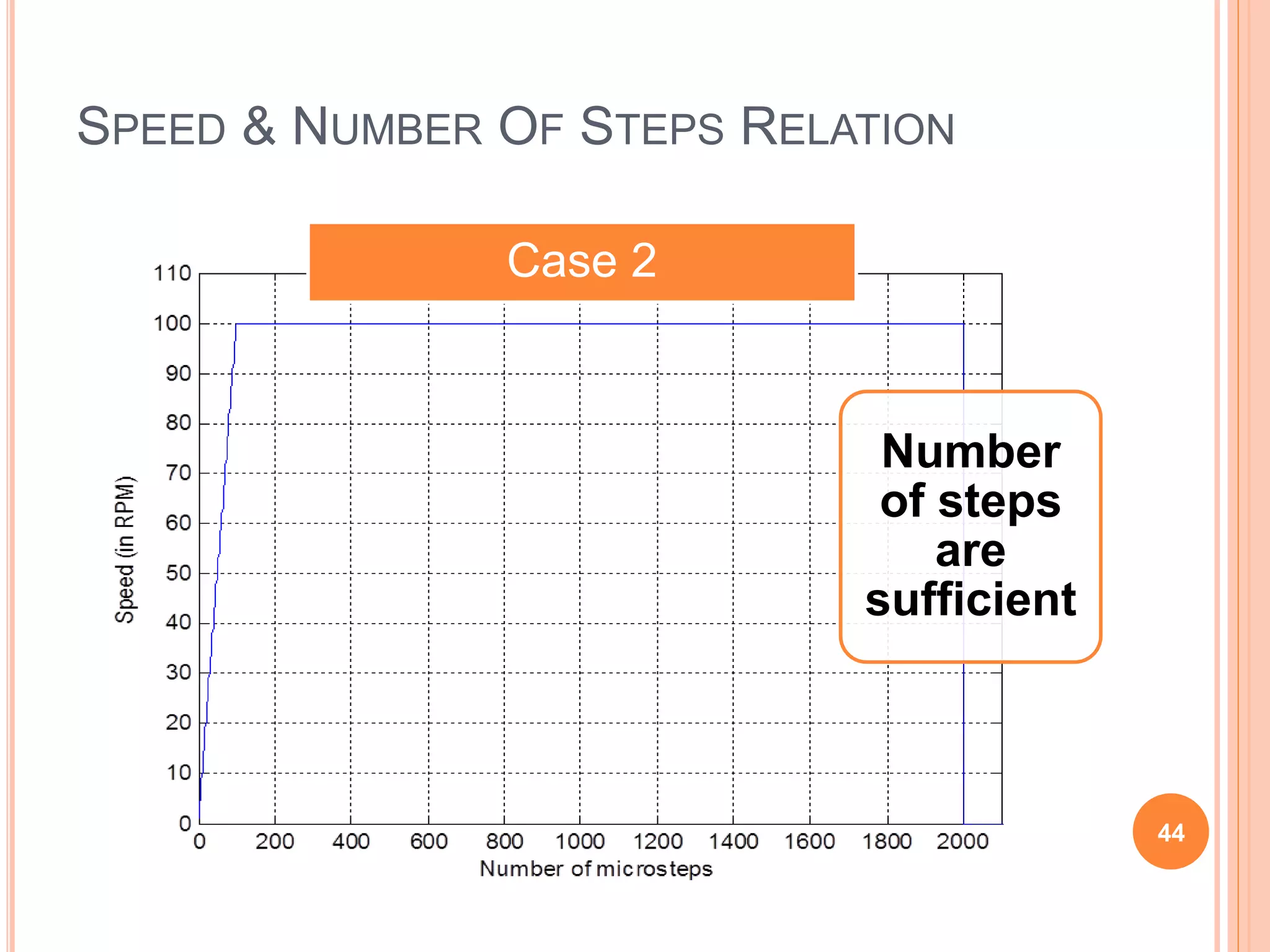
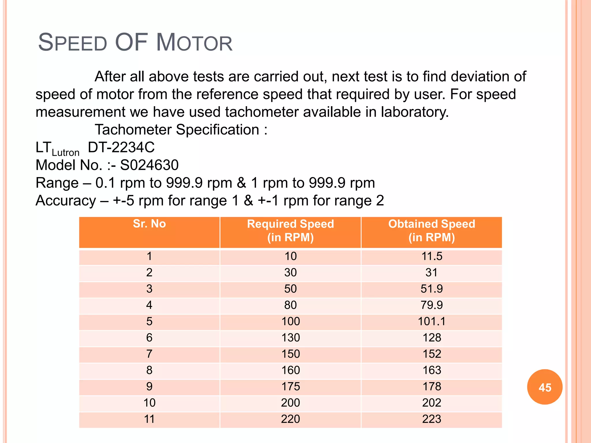
MICROSTEPPING OF STEPPER
MOTOR
(Sponsored Project by T.I.F.R. , Mumbai)
Presented by –
Tejas Mishra (B80393068)
Shrinath Thube (B80393119)
Anup Palarapwar (B80393146)
Under the guidance of
Prof. (Dr.) C. S. Garde
IN THIS PRESENTATION-
 Introduction
 Our AIM.
 Basic Working of Stepper Motor
 Specification of motor.
 Block Diagram.
 Selection of Component‘s
 Working of modules
 Schematics & Layouts
 Simulation Results
 Hardware Testing
 Relationship between speed & Timer Value
 Relationship between speed & Number of Steps
 Speed of Motor 2
INTRODUCTION
 Experiment at TIFR Mumbai.
 It requires extremely smooth motion and precise
positioning.
 Full-step and Half-step modes lead to very jerky
motion.
 Microstepping results in very smooth motion.
3
OUR AIM -
 Driving of Stepper motor in Micro-stepping mode.
 Step angle divide into 16 steps.
 RPM control upto 220 RPM
 Position control using limit switches.
4
BASIC WORKING OF BIPOLAR STEPPER
MOTOR
One
Phase
ON
Two
Phase
ON
Half
Phase
ON
Micro-
stepping
5
1. ONE PHASE ON
6
1.1 Current Flow Diagram
7
1.1 Current Flow Diagram
8
1.2 Voltage Waveform
2. TWO PHASE ON
2.1 Current Flow Diagram
9
2.2 Voltage Waveform
10
3. HALF PHASE ON
3.1 Current Flow Diagram
11
3.2 Voltage Waveform
12
4. MICROSTEPPING MODE
13
SPECIFICATION OF MOTOR
 Holding Torque – 120Ncm
 Motor Case Temperature: 100°C (212°F) max.
 Can operate at rates to 20,000 steps per second
(6000 rpm)
Motor Type No. of
Leads
Current
(Amps)
Voltage
(Vdc)
Resistance
(Ohms)
Inductance
(mH)
KML061F03 4 1.4 4.19 3 15.5
14
BLOCK DIAGRAM
15
SELECTION OF COMPONENTS
Parameter ATMEGA32 PIC18F452
PWM 4 2
Timers 4 3
EEPROM 1024b 256b
GPIO 32 32
ADC 8ch,10b 8ch,10b
Supply Voltage 2.7-5.5V 5V
1. Selection of Controller
Based on the above parameters we have selected Atmega 32 as it
is sufficient for our application.
16
Parameter IRF540 IRF640 IRF840
Vdss(V) 100 200 500
Id(A) 33 18 8
Rds(ohm) 44m 150m 850m
Vgs(th) 4 4 4
Pd(Tc=323K) 110W 125W 100W
Turn-on time 46ns 30ns 37ns
Turn-off time 74ns 30ns 69ns
2. Selection of Switch
Based on the above parameters we have selected IRF540
as it is sufficient for our application.
17
Parameter IR2104 IR2110
Deadtime 0.5us Not available
Io 200mA 1A
Iqbs 55uA 230uA
Delay matching Yes Yes
Turn-on time 0.6us 0.12us
Turn-off time 0.15us 0.1us
3. Selection of Driver Controller
Based on the above parameters we have selected IR2104 as
it is sufficient for our application.
18
WORKING OF MODULES
1. Working of H-Bridge Driver
19
2. Working of Controller
Atmega32
20
PIN CONFIGURATION OF CONTROLLER
Sr. No Requirement Pin used Description
1 Motor Windings
Winding 1
Winding 2
Winding 3
Winding 4
Pin C2
Pin C1
Pin C3
Pin C0
Here pins PC0 to PC4 are set as output pins
which sets motor position.
2 LCD
Data pin D4
Data pin D5
Data pin D6
Data pin D7
Register Select
Enable
Read/Write
Pin C4
Pin C5
Pin C6
Pin C7
Pin D4
Pin D5
Ground
Here pins PC0 to PC4 & PB0 to PB1 are set
as output pins which send data to LCD & for
R/S & E. R/W is directly grounded.
3 Limit Switches
End 1
End 2
Pin D2
Pin D3
Two external interrupts are used here,
response at falling edge to detect the end
position
4 PWM
PWM1
PWM2
Pin B3
Pin D7
Two 8 bit PWM are used here to control the
current through windings.
5 Keypad
Row 1
Row 2
Row 3
Column 1
Column 2
Column 3
Pin A5
Pin A6
Pin A7
Pin A2
Pin A3
Pin A4
Here we have used 3X3 keypad. For this pin
PA2 to PA7 are used as input pins which take
inputs like number of steps and maximum
speed (in RPM) from users and feed to
controller.
21
Supply 1
• Regulated
power
supply for
controller
(5V)
Supply 2
• Regulated
power
supply for H
bridge (12V)
Supply 3
• Unregulated
power
supply for
motor
windings (0-
34V)
3. Power Supply
22
SCHEMATICS
 Schematic of Controller Board
B0
(XCK/T0)
1
B1
(T1)
2
B2
(INT2/AIN0)
3
B3
(OC0/AIN1)
4
B4
(SS)
5
B5
(MOSI)
6
B6
(MISO)
7
B7
(SCK)
8
RESET
9
XTAL2
1
2
XTAL1
1
3
D0
(RXD)
1
4
D1
(TXD)
1
5
D2
(INT0)
1
6
D3
(INT1)
1
7
D4
(OC1B)
1
8
D5
(OC1A)
1
9
D6
(IC1)
2
0
D7
(OC2)
2
1
C0
(SCL)
2
2
C1
(SDA)
2
3
C2
(TCK)
2
4
C3
(TMS)
2
5
C4
(TDO)
2
6
C5
(TDI)
2
7
C6
(TOSC1)
2
8
C7
(TOSC2)
2
9
A7
(ADC7)
3
3
A6
(ADC6)
3
4
A5
(ADC5)
3
5
A4
(ADC4)
3
6
A3
(ADC3)
3
7
A2
(ADC2)
3
8
A1
(ADC1)
3
9
A0
(ADC0)
4
0
VCC
1
0
G
N
D
1
1
AVCC
3
0
G
N
D
3
1
AREF
3
2
UC1
ATmega32A-U
1
2
Y
1
XTAL
2
2
p
F
C
C
5
C
a
2
2
p
F
C
C
6
C
a
G
N
D
1
2
3
4
5
6
7
8
9
1
0
P
C
4
Header
5X2
miso
+
5
G
N
D
G
N
D
G
N
D
G
N
D
N
C
reset
sck
mosi
2
3
1
SC2
SW-SDT
+
2
3
1
SC3
SW-SDT
1
0
K
R
C
2
Res2
LD1
LED1
+
5
G
N
D
1
0
4
C
C
2
C
a
1
0
4
C
C
3
C
a
3k3
Reset
Res2
+
5
reset
1
0
0
p
F
C
C
7
Cap2
G
N
D
1
2
3
4
5
6
7
8
9
1
0
1
1
1
2
1
3
1
4
1
5
1
6
P
C
1
Header
16
D
7
D
6
D
5
D
4
D
7
D
6
D
5
D
4
E
N
r
s
G
N
D
+
5
G
N
D
+
5
G
N
D
G
N
D
+
5
G
N
D
+12V
mosi
miso
sck
3
3
0
R
R
C
1
Res2
1
2
3
P
C
6
Header
3
+
5
A
1
G
N
D
A
0
A
1
A
2
A
3
A
5
A
4
A
2
A
3
A
4
A
5
B
2
G
N
D
D
2
D
3
D
2
D
3
+
5
+
5
+
5
G
N
D
G
N
D
PWM2
PWM1
OC1B
OC1A
IC1
B
4
A
6
A
7
PWM1
PWM2
W
R
PWM1
1
2
3
P
C
7
Header
3
1
2
3
P
C
8
Header
3
G
N
D
1
2
3
P
C
9
Header
3
+
5
G
N
D
B
2
A
6
A
7
DACSEL
B
2
1
0
4
C
C
4
C
a
1
0
0
p
F
C
C
9
Cap2
1
0
0
p
F
C
C
8
Cap2
1
K
RC10
Res2
1
K
RC11
Res2
+
5
+
5
1
K
RC12
Res2
1
0
0
p
F
C
C
1
Cap2
1
K
RC13
Res2
1
K
RC14
Res2
1
K
RC15
Res2
B
5
B
6
B
7
1
2
3
PC10
Header
3
+
5
A
0
G
N
D
SC1
SW-PB
1
2
3
4
5
6
7
P
C
3
Header
7
+
5
G
N
D
r
s
E
N
Int4
Int5
Int5
1
2
PJumper
Header
2
+
5
Int5
1
2
PJumper1
Header
2
+
5
Int4
A
1
1
2
3
4
5
6
7
8
9
1
0
P
C
2
Header
5X2
G
N
D
G
N
D
IN1
IN2
IN3
IN4
IN1
IN2
IN3
IN4
PWM1
PWM2
1
2
3
4
5
6
7
8
9
1
0
P
C
5
Header
10
+
5
G
N
D
OUTA
OUTB
23
SCHEMATICS
 Schematic of Driver
VCC
1
COM
4
V
B
8
H
O
7
V
S
6
L
O
5
I
N
2
S
D
3
UM1
IR2104
VCC
1
COM
4
V
B
8
H
O
7
V
S
6
L
O
5
I
N
2
S
D
3
UM2
IR2104
DM9
Diode
1N914
DM10
Diode
1N914
470uF,25V
CM1
Cap
100uF,35v
CM7
Cap
1
0
4
CM8
Cap
100uF,35V
CM9
Cap
1
0
4
CM10
Cap
L
E
D
LED0
1
K
RM9
Res2
+12
SD1
IN1
G
N
D
+12
SD2
IN2
G
N
D
H
O
1
LO1
H
O
2
LO2
MT2
MT1
+12
G
N
D
G
N
D
MT1
MT2
+12
1
0
4
CM4
Cap
+12
G
N
D
1
0
4
CM5
Cap
+12
G
N
D
Q
2
IRF540N
Q
1
IRF540N
Q
4
IRF540N
Q
3
IRF540N
DM1
Diode
1N4937
DM2
Diode
1N4937
DM3
Diode
1N4937
DM4
Diode
1N4937
1
K
RM1
Res2
1
K
RM2
Res2
1
K
R
3
Res2
1
K
R
4
Res2
LO2
H
O
2
LO1
H
O
1
MT2
MT1
+Unreg
DM13
Diode
1N914
DM14
Diode
1N914
DM16
Diode
1N914
DM15
Diode
1N914
S
e
n
1
1
K
R10
Res2
-Unreg
Vb2
Vb1
G
2
G
1
G
4
G
3
VCC
1
COM
4
V
B
8
H
O
7
V
S
6
L
O
5
I
N
2
S
D
3
UM3
IR2104
VCC
1
COM
4
V
B
8
H
O
7
V
S
6
L
O
5
I
N
2
S
D
3
UM4
IR2104
DM11
Diode
1N914
DM12
Diode
1N914
100uF,35v
CM11
Cap
1
0
4
CM12
Cap
100uF,35V
CM13
Cap
1
0
4
CM14
Cap
+12
SD3
IN3
G
N
D
+12
SD4
IN4
G
N
D
H
O
3
LO3
H
O
4
LO4
MT4
MT3
MT3
MT4
Q
6
IRF540N
Q
5
IRF540N
Q
8
IRF540N
Q
7
IRF540N
DM5
Diode
1N4937
DM6
Diode
1N4937
DM7
Diode
14937
DM8
Diode
1N4937
1
K
R
5
Res2
1
K
R
6
Res2
1
K
R
7
Res2
1
K
R
8
Res2
LO4
H
O
4
LO3
H
O
3
MT4
MT3
+Unreg
DM17
Diode
1N914
DM18
Diode
1N914
DM20
Diode
1N914
DM19
Diode
1N914
S
e
n
2
1
K
R11
Res2
-Unreg
Vb4
Vb3
G
6
G
5
G
8
G
7
1
0
4
CM2
Cap
+12
G
N
D
1
0
4
CM3
Cap
+12
G
N
D
1
2
3
4
P
7
Header
4
-Unreg
-Unreg
SD2
SD1
1
2
3
4
5
6
7
8
9
1
0
PM1
Header
5X2
G
N
D
G
N
D
SD3
SD4
24
SCHEMATICS
 Schematic of Power Supply
1
2
P
P
1
Input-Unreg
1
2
3
4
P
P
3
6A
Rectifier
1
2
3
P
P
5
LM350
1
2
3
P
P
6
7
8
0
5
1
2
3
P
P
7
7
9
1
2
+Unreg
-Unreg
+12Ac
+
-
-12Ac
+Unreg
-Unreg
G
N
D
-
G
N
D
+12
G
N
D
+
5
G
N
D
-
-12
1
2
3
P
P
2
Input-12
+12Ac
G
N
D
-12Ac
+
0.22uF,50V
C
P
8
Cap2
0.22uF,50V
C
P
9
Cap2
+12
G
N
D
+
5
G
N
D
G
N
D
-12
G
N
D
1
0
0
p
F
CP10
Cap
1
0
0
p
F
CP11
Cap
1
0
0
p
F
CP12
Cap
1
0
0
p
F
C
P
1
Cap2
1
0
0
p
F
C
P
3
Cap2
1
0
0
p
F
C
P
4
Cap2
1
0
0
p
F
C
P
6
Cap2
-
1
K
R
P
1
Res2
1
K
R
P
2
Res2
1
K
R
P
3
Res2
1
K
R
P
5
Res2
100uF,25V
CP13
Cap2
100uF,25V
CP14
Cap2
+12
G
N
D
+
5
G
N
D
-
1
0
0
p
F
C
P
2
Cap2
+12
+12V
0.22uF,50V
CP15
Cap2
G
N
D
G
N
D
+12
+
25
LAYOUTS
 Top Layout
26
LAYOUTS
 Bottom Layout
27
SIMULATION RESULTS
 Winding State
28
 PWM Waveforms
29
 Current through Motor Winding
30
 LCD Sequence
31
HARDWARE TESTING
 Reference Waveform from IR2104 Datasheet
32
HARDWARE TESTING
1. Input & PWM waveform
Here channel 1 represents state of one winding of stepper
motor and winding 2 represents PWM value which is connected to
SD of IR2104.
33
1. Input and PWM waveform
This is zoom in view of input and PWM waveform 34
2. Input and Low side gate drive output
Here channel 1 represents state of one winding whereas channel 2
represents low side gate drive output of IR2104. It is exactly same as
reference waveform given in datasheet of IR2104.
Voltage range (peak to peak) :- 1) Input wave – 5V
2) Low side driver – 12V
35
3. Input and High side gate drive output
Here channel 1 represents state of one winding whereas channel 2 represents
high side gate drive output of IR2104. It is exactly same as reference waveform
given in datasheet of IR2104.
Voltage range (peak to peak) :- 1) Input wave – 5V
2) High side driver – 35V
36
4. Current through winding and PWM
In this waveform, channel 1 represents the current through motor winding
whereas channel 2 represents corresponding PWM waveform. Current
through winding follows shape like sin wave which represents that current
through winding is increase and then decrease smoothly. Thus there is
smooth variation in rotor position and microstepping is achieved.
37
5. Current through motor windings
38
5. Current through motor windings
In this waveform, channel 1 and channel 2 represents variation
of current through two motor windings. Both waveforms shows that
current through windings follows sine wave which are 900 in phase shift
with respect to each other.
39
RELATIONSHIP BETWEEN SPEED & TIMER
VALUE
0 1 2 3 4 5 6
x 10
4
0
50
100
150
200
Timer Value
Speed(inRPM)
Speed vs Timer Value
40
RELATIONSHIP BETWEEN SPEED &
TIMER VALUE
In this project, we have used 16 bit timer to control the speed of
motor. Thus by varying value to be laoded in register TCNT1 (Timer/Counter
register 1), speed of motor can be control. Relationship between speed and
value to be loaded in TCNT1 can be represent by following formula:
This relationship between can also represent with the help of graph. In this
graph, X axis represents the value that should be loaded in TCNT1 and Y axis
represents the speed of motor in RPM.
41
SPEED & NUMBER OF STEPS RELATION
• In this case, number of micro-steps are not
sufficient for motor to reach to its required
speed. Thus number of micro-steps that
motor is suppose to travel are completed
by motor before reaching to the required
speed.
Case 1 :
Number of
steps are
not
sufficient
• In this case, number of micro-steps are
sufficient for motor to reach to its required
speed. Thus before completing the number
of micro-steps that motor is supposed to
travel are completed by motor after
reaching to the required speed.
Case 2 :
Number of
steps are
sufficient 42
SPEED & NUMBER OF STEPS RELATION
Number
of steps
are not
sufficient
Case 1
43
SPEED & NUMBER OF STEPS RELATION
Number
of steps
are
sufficient
Case 2
44
SPEED OF MOTOR
After all above tests are carried out, next test is to find deviation of
speed of motor from the reference speed that required by user. For speed
measurement we have used tachometer available in laboratory.
Tachometer Specification :
LTLutron DT-2234C
Model No. :- S024630
Range – 0.1 rpm to 999.9 rpm & 1 rpm to 999.9 rpm
Accuracy – +-5 rpm for range 1 & +-1 rpm for range 2
Sr. No Required Speed
(in RPM)
Obtained Speed
(in RPM)
1 10 11.5
2 30 31
3 50 51.9
4 80 79.9
5 100 101.1
6 130 128
7 150 152
8 160 163
9 175 178
10 200 202
11 220 223
45
THANK YOU
46

Microstepping of stepper Motor

  • 1.
    MICROSTEPPING OF STEPPER MOTOR (SponsoredProject by T.I.F.R. , Mumbai) Presented by – Tejas Mishra (B80393068) Shrinath Thube (B80393119) Anup Palarapwar (B80393146) Under the guidance of Prof. (Dr.) C. S. Garde
  • 2.
    IN THIS PRESENTATION- Introduction  Our AIM.  Basic Working of Stepper Motor  Specification of motor.  Block Diagram.  Selection of Component‘s  Working of modules  Schematics & Layouts  Simulation Results  Hardware Testing  Relationship between speed & Timer Value  Relationship between speed & Number of Steps  Speed of Motor 2
  • 3.
    INTRODUCTION  Experiment atTIFR Mumbai.  It requires extremely smooth motion and precise positioning.  Full-step and Half-step modes lead to very jerky motion.  Microstepping results in very smooth motion. 3
  • 4.
    OUR AIM - Driving of Stepper motor in Micro-stepping mode.  Step angle divide into 16 steps.  RPM control upto 220 RPM  Position control using limit switches. 4
  • 5.
    BASIC WORKING OFBIPOLAR STEPPER MOTOR One Phase ON Two Phase ON Half Phase ON Micro- stepping 5
  • 6.
    1. ONE PHASEON 6 1.1 Current Flow Diagram
  • 7.
  • 8.
  • 9.
    2. TWO PHASEON 2.1 Current Flow Diagram 9
  • 10.
  • 11.
    3. HALF PHASEON 3.1 Current Flow Diagram 11
  • 12.
  • 13.
  • 14.
    SPECIFICATION OF MOTOR Holding Torque – 120Ncm  Motor Case Temperature: 100°C (212°F) max.  Can operate at rates to 20,000 steps per second (6000 rpm) Motor Type No. of Leads Current (Amps) Voltage (Vdc) Resistance (Ohms) Inductance (mH) KML061F03 4 1.4 4.19 3 15.5 14
  • 15.
  • 16.
    SELECTION OF COMPONENTS ParameterATMEGA32 PIC18F452 PWM 4 2 Timers 4 3 EEPROM 1024b 256b GPIO 32 32 ADC 8ch,10b 8ch,10b Supply Voltage 2.7-5.5V 5V 1. Selection of Controller Based on the above parameters we have selected Atmega 32 as it is sufficient for our application. 16
  • 17.
    Parameter IRF540 IRF640IRF840 Vdss(V) 100 200 500 Id(A) 33 18 8 Rds(ohm) 44m 150m 850m Vgs(th) 4 4 4 Pd(Tc=323K) 110W 125W 100W Turn-on time 46ns 30ns 37ns Turn-off time 74ns 30ns 69ns 2. Selection of Switch Based on the above parameters we have selected IRF540 as it is sufficient for our application. 17
  • 18.
    Parameter IR2104 IR2110 Deadtime0.5us Not available Io 200mA 1A Iqbs 55uA 230uA Delay matching Yes Yes Turn-on time 0.6us 0.12us Turn-off time 0.15us 0.1us 3. Selection of Driver Controller Based on the above parameters we have selected IR2104 as it is sufficient for our application. 18
  • 19.
    WORKING OF MODULES 1.Working of H-Bridge Driver 19
  • 20.
    2. Working ofController Atmega32 20
  • 21.
    PIN CONFIGURATION OFCONTROLLER Sr. No Requirement Pin used Description 1 Motor Windings Winding 1 Winding 2 Winding 3 Winding 4 Pin C2 Pin C1 Pin C3 Pin C0 Here pins PC0 to PC4 are set as output pins which sets motor position. 2 LCD Data pin D4 Data pin D5 Data pin D6 Data pin D7 Register Select Enable Read/Write Pin C4 Pin C5 Pin C6 Pin C7 Pin D4 Pin D5 Ground Here pins PC0 to PC4 & PB0 to PB1 are set as output pins which send data to LCD & for R/S & E. R/W is directly grounded. 3 Limit Switches End 1 End 2 Pin D2 Pin D3 Two external interrupts are used here, response at falling edge to detect the end position 4 PWM PWM1 PWM2 Pin B3 Pin D7 Two 8 bit PWM are used here to control the current through windings. 5 Keypad Row 1 Row 2 Row 3 Column 1 Column 2 Column 3 Pin A5 Pin A6 Pin A7 Pin A2 Pin A3 Pin A4 Here we have used 3X3 keypad. For this pin PA2 to PA7 are used as input pins which take inputs like number of steps and maximum speed (in RPM) from users and feed to controller. 21
  • 22.
    Supply 1 • Regulated power supplyfor controller (5V) Supply 2 • Regulated power supply for H bridge (12V) Supply 3 • Unregulated power supply for motor windings (0- 34V) 3. Power Supply 22
  • 23.
    SCHEMATICS  Schematic ofController Board B0 (XCK/T0) 1 B1 (T1) 2 B2 (INT2/AIN0) 3 B3 (OC0/AIN1) 4 B4 (SS) 5 B5 (MOSI) 6 B6 (MISO) 7 B7 (SCK) 8 RESET 9 XTAL2 1 2 XTAL1 1 3 D0 (RXD) 1 4 D1 (TXD) 1 5 D2 (INT0) 1 6 D3 (INT1) 1 7 D4 (OC1B) 1 8 D5 (OC1A) 1 9 D6 (IC1) 2 0 D7 (OC2) 2 1 C0 (SCL) 2 2 C1 (SDA) 2 3 C2 (TCK) 2 4 C3 (TMS) 2 5 C4 (TDO) 2 6 C5 (TDI) 2 7 C6 (TOSC1) 2 8 C7 (TOSC2) 2 9 A7 (ADC7) 3 3 A6 (ADC6) 3 4 A5 (ADC5) 3 5 A4 (ADC4) 3 6 A3 (ADC3) 3 7 A2 (ADC2) 3 8 A1 (ADC1) 3 9 A0 (ADC0) 4 0 VCC 1 0 G N D 1 1 AVCC 3 0 G N D 3 1 AREF 3 2 UC1 ATmega32A-U 1 2 Y 1 XTAL 2 2 p F C C 5 C a 2 2 p F C C 6 C a G N D 1 2 3 4 5 6 7 8 9 1 0 P C 4 Header 5X2 miso + 5 G N D G N D G N D G N D N C reset sck mosi 2 3 1 SC2 SW-SDT + 2 3 1 SC3 SW-SDT 1 0 K R C 2 Res2 LD1 LED1 + 5 G N D 1 0 4 C C 2 C a 1 0 4 C C 3 C a 3k3 Reset Res2 + 5 reset 1 0 0 p F C C 7 Cap2 G N D 1 2 3 4 5 6 7 8 9 1 0 1 1 1 2 1 3 1 4 1 5 1 6 P C 1 Header 16 D 7 D 6 D 5 D 4 D 7 D 6 D 5 D 4 E N r s G N D + 5 G N D + 5 G N D G N D + 5 G N D +12V mosi miso sck 3 3 0 R R C 1 Res2 1 2 3 P C 6 Header 3 + 5 A 1 G N D A 0 A 1 A 2 A 3 A 5 A 4 A 2 A 3 A 4 A 5 B 2 G N D D 2 D 3 D 2 D 3 + 5 + 5 + 5 G N D G N D PWM2 PWM1 OC1B OC1A IC1 B 4 A 6 A 7 PWM1 PWM2 W R PWM1 1 2 3 P C 7 Header 3 1 2 3 P C 8 Header 3 G N D 1 2 3 P C 9 Header 3 + 5 G N D B 2 A 6 A 7 DACSEL B 2 1 0 4 C C 4 C a 1 0 0 p F C C 9 Cap2 1 0 0 p F C C 8 Cap2 1 K RC10 Res2 1 K RC11 Res2 + 5 + 5 1 K RC12 Res2 1 0 0 p F C C 1 Cap2 1 K RC13 Res2 1 K RC14 Res2 1 K RC15 Res2 B 5 B 6 B 7 1 2 3 PC10 Header 3 + 5 A 0 G N D SC1 SW-PB 1 2 3 4 5 6 7 P C 3 Header 7 + 5 G N D r s E N Int4 Int5 Int5 1 2 PJumper Header 2 + 5 Int5 1 2 PJumper1 Header 2 + 5 Int4 A 1 1 2 3 4 5 6 7 8 9 1 0 P C 2 Header 5X2 G N D G N D IN1 IN2 IN3 IN4 IN1 IN2 IN3 IN4 PWM1 PWM2 1 2 3 4 5 6 7 8 9 1 0 P C 5 Header 10 + 5 G N D OUTA OUTB 23
  • 24.
    SCHEMATICS  Schematic ofDriver VCC 1 COM 4 V B 8 H O 7 V S 6 L O 5 I N 2 S D 3 UM1 IR2104 VCC 1 COM 4 V B 8 H O 7 V S 6 L O 5 I N 2 S D 3 UM2 IR2104 DM9 Diode 1N914 DM10 Diode 1N914 470uF,25V CM1 Cap 100uF,35v CM7 Cap 1 0 4 CM8 Cap 100uF,35V CM9 Cap 1 0 4 CM10 Cap L E D LED0 1 K RM9 Res2 +12 SD1 IN1 G N D +12 SD2 IN2 G N D H O 1 LO1 H O 2 LO2 MT2 MT1 +12 G N D G N D MT1 MT2 +12 1 0 4 CM4 Cap +12 G N D 1 0 4 CM5 Cap +12 G N D Q 2 IRF540N Q 1 IRF540N Q 4 IRF540N Q 3 IRF540N DM1 Diode 1N4937 DM2 Diode 1N4937 DM3 Diode 1N4937 DM4 Diode 1N4937 1 K RM1 Res2 1 K RM2 Res2 1 K R 3 Res2 1 K R 4 Res2 LO2 H O 2 LO1 H O 1 MT2 MT1 +Unreg DM13 Diode 1N914 DM14 Diode 1N914 DM16 Diode 1N914 DM15 Diode 1N914 S e n 1 1 K R10 Res2 -Unreg Vb2 Vb1 G 2 G 1 G 4 G 3 VCC 1 COM 4 V B 8 H O 7 V S 6 L O 5 I N 2 S D 3 UM3 IR2104 VCC 1 COM 4 V B 8 H O 7 V S 6 L O 5 I N 2 S D 3 UM4 IR2104 DM11 Diode 1N914 DM12 Diode 1N914 100uF,35v CM11 Cap 1 0 4 CM12 Cap 100uF,35V CM13 Cap 1 0 4 CM14 Cap +12 SD3 IN3 G N D +12 SD4 IN4 G N D H O 3 LO3 H O 4 LO4 MT4 MT3 MT3 MT4 Q 6 IRF540N Q 5 IRF540N Q 8 IRF540N Q 7 IRF540N DM5 Diode 1N4937 DM6 Diode 1N4937 DM7 Diode 14937 DM8 Diode 1N4937 1 K R 5 Res2 1 K R 6 Res2 1 K R 7 Res2 1 K R 8 Res2 LO4 H O 4 LO3 H O 3 MT4 MT3 +Unreg DM17 Diode 1N914 DM18 Diode 1N914 DM20 Diode 1N914 DM19 Diode 1N914 S e n 2 1 K R11 Res2 -Unreg Vb4 Vb3 G 6 G 5 G 8 G 7 1 0 4 CM2 Cap +12 G N D 1 0 4 CM3 Cap +12 G N D 1 2 3 4 P 7 Header 4 -Unreg -Unreg SD2 SD1 1 2 3 4 5 6 7 8 9 1 0 PM1 Header 5X2 G N D G N D SD3 SD4 24
  • 25.
    SCHEMATICS  Schematic ofPower Supply 1 2 P P 1 Input-Unreg 1 2 3 4 P P 3 6A Rectifier 1 2 3 P P 5 LM350 1 2 3 P P 6 7 8 0 5 1 2 3 P P 7 7 9 1 2 +Unreg -Unreg +12Ac + - -12Ac +Unreg -Unreg G N D - G N D +12 G N D + 5 G N D - -12 1 2 3 P P 2 Input-12 +12Ac G N D -12Ac + 0.22uF,50V C P 8 Cap2 0.22uF,50V C P 9 Cap2 +12 G N D + 5 G N D G N D -12 G N D 1 0 0 p F CP10 Cap 1 0 0 p F CP11 Cap 1 0 0 p F CP12 Cap 1 0 0 p F C P 1 Cap2 1 0 0 p F C P 3 Cap2 1 0 0 p F C P 4 Cap2 1 0 0 p F C P 6 Cap2 - 1 K R P 1 Res2 1 K R P 2 Res2 1 K R P 3 Res2 1 K R P 5 Res2 100uF,25V CP13 Cap2 100uF,25V CP14 Cap2 +12 G N D + 5 G N D - 1 0 0 p F C P 2 Cap2 +12 +12V 0.22uF,50V CP15 Cap2 G N D G N D +12 + 25
  • 26.
  • 27.
  • 28.
  • 29.
  • 30.
     Current throughMotor Winding 30
  • 31.
  • 32.
    HARDWARE TESTING  ReferenceWaveform from IR2104 Datasheet 32
  • 33.
    HARDWARE TESTING 1. Input& PWM waveform Here channel 1 represents state of one winding of stepper motor and winding 2 represents PWM value which is connected to SD of IR2104. 33
  • 34.
    1. Input andPWM waveform This is zoom in view of input and PWM waveform 34
  • 35.
    2. Input andLow side gate drive output Here channel 1 represents state of one winding whereas channel 2 represents low side gate drive output of IR2104. It is exactly same as reference waveform given in datasheet of IR2104. Voltage range (peak to peak) :- 1) Input wave – 5V 2) Low side driver – 12V 35
  • 36.
    3. Input andHigh side gate drive output Here channel 1 represents state of one winding whereas channel 2 represents high side gate drive output of IR2104. It is exactly same as reference waveform given in datasheet of IR2104. Voltage range (peak to peak) :- 1) Input wave – 5V 2) High side driver – 35V 36
  • 37.
    4. Current throughwinding and PWM In this waveform, channel 1 represents the current through motor winding whereas channel 2 represents corresponding PWM waveform. Current through winding follows shape like sin wave which represents that current through winding is increase and then decrease smoothly. Thus there is smooth variation in rotor position and microstepping is achieved. 37
  • 38.
    5. Current throughmotor windings 38
  • 39.
    5. Current throughmotor windings In this waveform, channel 1 and channel 2 represents variation of current through two motor windings. Both waveforms shows that current through windings follows sine wave which are 900 in phase shift with respect to each other. 39
  • 40.
    RELATIONSHIP BETWEEN SPEED& TIMER VALUE 0 1 2 3 4 5 6 x 10 4 0 50 100 150 200 Timer Value Speed(inRPM) Speed vs Timer Value 40
  • 41.
    RELATIONSHIP BETWEEN SPEED& TIMER VALUE In this project, we have used 16 bit timer to control the speed of motor. Thus by varying value to be laoded in register TCNT1 (Timer/Counter register 1), speed of motor can be control. Relationship between speed and value to be loaded in TCNT1 can be represent by following formula: This relationship between can also represent with the help of graph. In this graph, X axis represents the value that should be loaded in TCNT1 and Y axis represents the speed of motor in RPM. 41
  • 42.
    SPEED & NUMBEROF STEPS RELATION • In this case, number of micro-steps are not sufficient for motor to reach to its required speed. Thus number of micro-steps that motor is suppose to travel are completed by motor before reaching to the required speed. Case 1 : Number of steps are not sufficient • In this case, number of micro-steps are sufficient for motor to reach to its required speed. Thus before completing the number of micro-steps that motor is supposed to travel are completed by motor after reaching to the required speed. Case 2 : Number of steps are sufficient 42
  • 43.
    SPEED & NUMBEROF STEPS RELATION Number of steps are not sufficient Case 1 43
  • 44.
    SPEED & NUMBEROF STEPS RELATION Number of steps are sufficient Case 2 44
  • 45.
    SPEED OF MOTOR Afterall above tests are carried out, next test is to find deviation of speed of motor from the reference speed that required by user. For speed measurement we have used tachometer available in laboratory. Tachometer Specification : LTLutron DT-2234C Model No. :- S024630 Range – 0.1 rpm to 999.9 rpm & 1 rpm to 999.9 rpm Accuracy – +-5 rpm for range 1 & +-1 rpm for range 2 Sr. No Required Speed (in RPM) Obtained Speed (in RPM) 1 10 11.5 2 30 31 3 50 51.9 4 80 79.9 5 100 101.1 6 130 128 7 150 152 8 160 163 9 175 178 10 200 202 11 220 223 45
  • 46.