Download to read offline
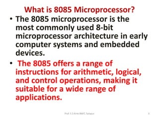
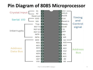


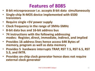


The 8085 microprocessor is an 8-bit microprocessor architecture commonly used in early computer systems and embedded devices. It has an 8-bit data bus, 16-bit address bus, and features like serial I/O ports, interrupts, and on-chip clock generator. The 8085 has functional units like the ALU, control unit, and instruction decoder. It uses general purpose and special purpose registers like the accumulator, stack pointer, and program counter. The document discusses the pin diagram, architecture, and features of the 8085 microprocessor.