Download to read offline


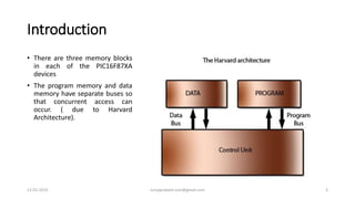
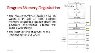
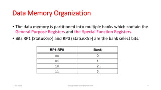

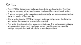


This document discusses the memory organization of the PIC16F876A/877A microcontroller. It describes the program memory, data memory, and special function registers. The program memory is 8K words by 14 bits and implements a reset vector at address 0000h and interrupt vector at 0004h. The data memory is partitioned into banks selected by bits in the status register. Special function registers like the status, PCL, PCLATH, and stack registers are also described. The document outlines how to access data EEPROM and flash program memory using various SFR registers.