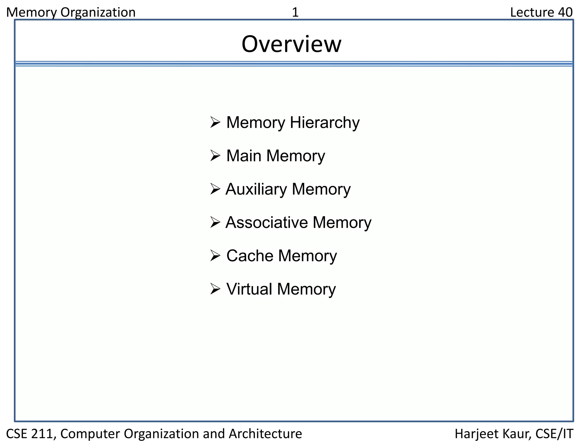
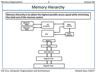
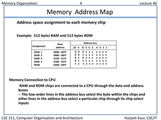
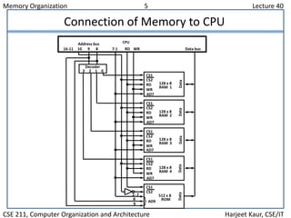
Memory Organization 1 Lecture 40
CSE 211, Computer Organization and Architecture Harjeet Kaur, CSE/IT
Overview
 Memory Hierarchy
 Main Memory
 Auxiliary Memory
 Associative Memory
 Cache Memory
 Virtual Memory
Memory Organization 2 Lecture 40
CSE 211, Computer Organization and Architecture Harjeet Kaur, CSE/IT
Memory Hierarchy
Magnetic
tapes
Magnetic
disks
I/O
processor
CPU
Main
memory
Cache
memory
Register
Cache
Main Memory
Magnetic Disk
Magnetic Tape
Memory Hierarchy is to obtain the highest possible access speed while minimizing
the total cost of the memory system
Memory Organization 3 Lecture 40
CSE 211, Computer Organization and Architecture Harjeet Kaur, CSE/IT
Main Memory
RAM and ROM Chips
Typical RAM chip
Typical ROM chip
Chip select 1
Chip select 2
Read
Write
7-bit address
CS1
CS2
RD
WR
AD 7
128 x 8
RAM
8-bit data bus
CS1 CS2 RD WR
0 0 x x
0 1 x x
1 0 0 0
1 0 0 1
1 0 1 x
1 1 x x
Memory function
Inhibit
Inhibit
Inhibit
Write
Read
Inhibit
State of data bus
High-impedence
High-impedence
High-impedence
Input data to RAM
Output data from RAM
High-impedence
Chip select 1
Chip select 2
9-bit address
CS1
CS2
AD 9
512 x 8
ROM
8-bit data bus
Memory Organization 4 Lecture 40
CSE 211, Computer Organization and Architecture Harjeet Kaur, CSE/IT
Memory Address Map
Address space assignment to each memory chip
Example: 512 bytes RAM and 512 bytes ROM
RAM 1
RAM 2
RAM 3
RAM 4
ROM
0000 - 007F
0080 - 00FF
0100 - 017F
0180 - 01FF
0200 - 03FF
Component
Hexa
address
0 0 0 x x x x x x x
0 0 1 x x x x x x x
0 1 0 x x x x x x x
0 1 1 x x x x x x x
1 x x x x x x x x x
10 9 8 7 6 5 4 3 2 1
Address bus
Memory Connection to CPU
-RAM and ROM chips are connected to a CPU through the data and address
buses
-- The low-order lines in the address bus select the byte within the chips and
other lines in the address bus select a particular chip through its chip select
inputs
Memory Organization 5 Lecture 40
CSE 211, Computer Organization and Architecture Harjeet Kaur, CSE/IT
Connection of Memory to CPU
}
CS1
CS2
RD
WR
AD7
128 x 8
RAM 1
CS1
CS2
RD
WR
AD7
128 x 8
RAM 2
CS1
CS2
RD
WR
AD7
128 x 8
RAM 3
CS1
CS2
RD
WR
AD7
128 x 8
RAM 4
Decoder
3 2 1 0
WRRD9 8 7-11016-11
Address bus
Data bus
CPU
CS1
CS2
512 x 8
ROMAD9
1- 7
9
8
DataDataDataDataData
Memory Organization 6 Lecture 40
CSE 211, Computer Organization and Architecture Harjeet Kaur, CSE/IT
Connection of Memory to CPU

Lecture 40

  • 1.
    Memory Organization 1Lecture 40 CSE 211, Computer Organization and Architecture Harjeet Kaur, CSE/IT Overview  Memory Hierarchy  Main Memory  Auxiliary Memory  Associative Memory  Cache Memory  Virtual Memory
  • 2.
    Memory Organization 2Lecture 40 CSE 211, Computer Organization and Architecture Harjeet Kaur, CSE/IT Memory Hierarchy Magnetic tapes Magnetic disks I/O processor CPU Main memory Cache memory Register Cache Main Memory Magnetic Disk Magnetic Tape Memory Hierarchy is to obtain the highest possible access speed while minimizing the total cost of the memory system
  • 3.
    Memory Organization 3Lecture 40 CSE 211, Computer Organization and Architecture Harjeet Kaur, CSE/IT Main Memory RAM and ROM Chips Typical RAM chip Typical ROM chip Chip select 1 Chip select 2 Read Write 7-bit address CS1 CS2 RD WR AD 7 128 x 8 RAM 8-bit data bus CS1 CS2 RD WR 0 0 x x 0 1 x x 1 0 0 0 1 0 0 1 1 0 1 x 1 1 x x Memory function Inhibit Inhibit Inhibit Write Read Inhibit State of data bus High-impedence High-impedence High-impedence Input data to RAM Output data from RAM High-impedence Chip select 1 Chip select 2 9-bit address CS1 CS2 AD 9 512 x 8 ROM 8-bit data bus
  • 4.
    Memory Organization 4Lecture 40 CSE 211, Computer Organization and Architecture Harjeet Kaur, CSE/IT Memory Address Map Address space assignment to each memory chip Example: 512 bytes RAM and 512 bytes ROM RAM 1 RAM 2 RAM 3 RAM 4 ROM 0000 - 007F 0080 - 00FF 0100 - 017F 0180 - 01FF 0200 - 03FF Component Hexa address 0 0 0 x x x x x x x 0 0 1 x x x x x x x 0 1 0 x x x x x x x 0 1 1 x x x x x x x 1 x x x x x x x x x 10 9 8 7 6 5 4 3 2 1 Address bus Memory Connection to CPU -RAM and ROM chips are connected to a CPU through the data and address buses -- The low-order lines in the address bus select the byte within the chips and other lines in the address bus select a particular chip through its chip select inputs
  • 5.
    Memory Organization 5Lecture 40 CSE 211, Computer Organization and Architecture Harjeet Kaur, CSE/IT Connection of Memory to CPU } CS1 CS2 RD WR AD7 128 x 8 RAM 1 CS1 CS2 RD WR AD7 128 x 8 RAM 2 CS1 CS2 RD WR AD7 128 x 8 RAM 3 CS1 CS2 RD WR AD7 128 x 8 RAM 4 Decoder 3 2 1 0 WRRD9 8 7-11016-11 Address bus Data bus CPU CS1 CS2 512 x 8 ROMAD9 1- 7 9 8 DataDataDataDataData
  • 6.
    Memory Organization 6Lecture 40 CSE 211, Computer Organization and Architecture Harjeet Kaur, CSE/IT Connection of Memory to CPU