Download to read offline


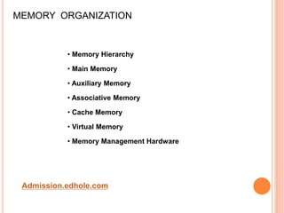
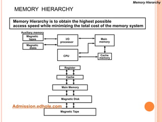
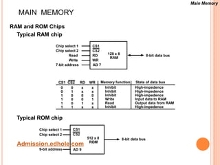
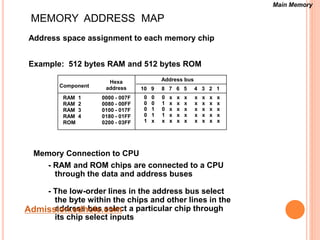
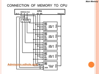

This document discusses memory organization and hierarchy. It describes the different types of memory including main memory, auxiliary memory, associative memory, cache memory, and virtual memory. It focuses on main memory, explaining RAM and ROM chips, how they are addressed and mapped in memory, and how memory is connected to the CPU via address and data buses. RAM and ROM chips are selected using chip select lines, while addresses select the byte location. Memory is mapped into blocks that each chip can access.