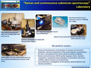
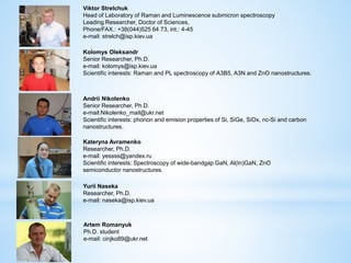
Laboratory
«Raman and Luminescence Submicron
Spectroscopy»
V. Lashkaryov Institute of Semiconductor Physics
National Academy of Science, Ukraine
41, pr. Nauky, Kyiv, Ukraine, 03028
National Academy of Science,
Ukraine www.microscopy.org.ua
“Raman and Luminescence submicron spectroscopy”
Laboratory
Lasers: HeCd (325 nm), Nd:YAG (355 nm) Ar-Kr
laser Stabilite 2018-RM Spectra Physics 2.5W
(USA);
Triple spectrometer Horiba
Jobin-Yvon T64000 (200÷1700
nm) (France);
Confocal microscope UV-Visible-NIR
Olympus BX41 (Japan);
XYZ motorized stage with step 0,1
mkm (Німечина);
Optical microcryostat RC102-CFM (3.5÷325К) (CIA
CRYO Industries, USA);
Microthermoelectrical cell
Linkam Sci. Instrum. THMS600
(78 ÷ 900K).
• Raman and luminescence microanalysis of emission and structural
properties, chemical composition of the semiconductor nanostructures
for micro- and optoelectronics with submicron spatial resolution.
• Raman and luminescence 2D-3D spatial mapping: strains, chemical
composition, temperature (thermography); concentration and carrier
mobility; optical emission of nanostructures;
• Low temperature investigations of the phonon, plasmon-phonon and
electron excitations.
We perform studies :
www.microscopy.org.ua
Our Team
Kolomys Oleksandr
Senior Researcher, Ph.D.
e-mail: kolomys@isp.kiev.ua
Scientific interests: Raman and PL spectroscopy of А3В5, А3N and ZnO nanostructures.
Andrii Nikolenko
Senior Researcher, Ph.D.
e-mail:Nikolenko_mail@ukr.net
Scientific interests: phonon and emision properties of Si, SiGe, SiOx, nc-Si and carbon
nanostructures.
Kateryna Avramenko
Researcher, Ph.D.
e-mail: yessss@yandex.ru
Scientific interests: Spectroscopy of wide-bandgap GaN, Al(In)GaN, ZnO
semiconductor nanostructures.
Yurii Naseka
Researcher, Ph.D.
e-mail: naseka@isp.kiev.ua
Viktor Strelchuk
Head of Laboratory of Raman and Luminescence submicron spectroscopy
Leading Researcher, Doctor of Sciences,
Phone/FAX.: +38(044)525 64 73, int.: 4-45
e-mail: strelch@isp.kiev.ua
Artem Romanyuk
Ph.D. student
e-mail: cinjko89@ukr.net
InGaAs QD
Areas of interests
Semiconductor
nanomaterials
Carbon nanostructures
(nanotubes, graphene,
diamond, poly-diamond,
DLC, fullerenes, TiC, SiC)
Bionanomaterials
(cancer, SERS)
Chemical synthesis
Si, Ge, SiGe
(nanowires, quantum dots)
nano
Nitrides
(GaN, InGaN, AlN)
A3B5
(AlGaAs, InAs/InGaAs)
Si nanowires
Colloidal quantum dots
A2B6 nanostructures
(colloidal quantum dots)
Polycrystalline diamond films
Energy,eV
Intensity,arb.un.
LED InGaN
multilayered structures
In Cooperation with:
Ecole Superieure de Physique et de Chimie Industrielles,
CNRS, Paris, France
P.Tronc
Centre de Recherches sur l’Heteroepitaxie et ses Applications,
CNRS, Valbone, France
C. Deparis, Christian Morhain
Institute of microstructure physics RAS
Z.F. Krasilnik, A.V. Novikov
University of Arkansas, USA
G.J. Salamo,Yu.I. Mazur, Zh.M. Wang
Institute of Physics of Semiconductors, RAS
T. Shamirzaev
Raman scattering - (combination light scattering) – nonelastic (with
frequency change) light scattering on environment phonon vibrations.
Was experimentally discovered
in February 1928г. in Calcutta
(India) by Sir Chandrasekhara
Venkata Rāman (Nature, 31
march 1928).
1930 г. – Raman was awarded by
Nobel Prize.
What is Raman scattering?
Electronstate
n = 0
n = 1
 = 0
 = 1
 = 3
Vibrational
state
IR
absorption
Relay
Raman
Stokes
Raman
AntiStokes
Resonant
Raman
Virtual state
Was simultaneously experimentally
discovered and theoretically
explained in February
1928г. in Moscow (USSR)
by L.I. Mandelshtam and
G.S. Landsberg
(Naturwissenschaften, 13
june 1928).
What can Raman Spectra tell us?
Band position:
Chemical
species,
symmetry Frequency Shift:
Strain,
temperature
Wavenumber or
Energy
Intensity:
Concentration
Width:
Structural
disorder
• Vibrational frequencies are characteristic of
chemical bonds or groups of bonds in a specific
molecule: normal modes
• Shifts of Vibrational frequencies are sensitive
to local environment of a molecule, such as
crystal phase, local strain, and degree of
crystallinity
=> A Raman spectrum provides a fingerprint
representing the set of bonds present in the
material
• Relative intensities within a spectrum can
quantify the orientation of a bond w.r.t. the
incoming laser polarization. The concentration of
a substance.
• Raman spectroscopy is complementary to IR.
What can confocal microspectroscopy give us?
o
2
Laser beam is focused to spot diameter d :
0.61
;
0.61 Relaycriterion
0.89
Focusdepth :
( )
od
NA
k
L
NA



 

For objective with
NA = 0.90; exc = 488 nm
d0 = 0.33 mm; L = 0.54 mm
Higher spatial resolution!XYZ – submicron spatial Raman mapping
Examples of confocal Raman and luminescence spectroscopy application
(spatial resolution 100 ÷ 500 nm)
Strain distribution in micro- and
nanoelectronics structures
Compression
Tension
-100
-50
0
-50
-100
-100
MPa
2x2 mm
Lipid, protein and starch content
in wheat grain
Photoluminescence control of laser
diode composition fluctuations
Phase distribution in
nanodiamond film
3000
2500
2000
1500
2800
2600
2400
2200
2000
1800
Intensity(counts/s)
30.5 31.0 31.5 32.0
Length X (µm)
350
nm
250
nm
3D Raman map intensity
distribution of Si-phonon band
SiO2 on Si (001)
In cooperation with:
• Ecole Superieure de Physique et de Chimie Industrielles, CNRS, Paris, France;
• Centre de Recherches sur l’Heteroepitaxie et ses Applications, CNRS, Valbone, France
=-40 K
=-200K
 Strong magnetic anisotropy: H//c, Hc
 easy-plane magnetization Hc (H//c)
expect at 5К (300K)
This work supported by NATO science programme, 2010-2011, NATO CLG 983878
Ferromagnetism in Co-doped ZnO films grown by molecular beam epitaxy: magnetic, electrical and microstructural
studies V.V. Strelchuk, V.P. Bryksa, K.A. Avramenko, P.M. Lytvyn, M.Ya. Valakh, V.O. Pashchenko, O.M. Bludov, C. Deparis, C.
Morhain, P. Tronc // Semiconductor Physics, Quantum Electronics & Optoelectronics 14, 1, 31-40 (2011).
French-Ukrainian science and technology cooperation program «Dnipro» on 2011 -2012 .
Submicron Raman and Photoluminescence Topography of InAs/Al(Ga)As
quantum dots structures O.F. Kolomys, V.V. Strelchuk, T.S. Shamirzaev, A.S.
Romanyuk, P. Tronc // Applied Surface Science 260, 47-50 (2012).
Molecule of dye
cyanine C29H33N2IFörster resonance energy transfer (FRET)
Eabsorp
PL
Eexc
PL
Donor Acceptor
Eabsorp
PL
AlAs
barrier
Indirect
InAs QD
GaAs substrate
In cooperation with:
• Ecole Superieure de Physique et de Chimie Industrielles, CNRS, Paris, France;
• Institute of Physics of Semiconductors, RAS, Novosibirsk, Russia
210
240
270
300
330
360
390
420
Raman shift (cm -1
)
AlAs-like group
InAs-like group
GaAs-like group
Substrate
Surface
Raman and photoluminescence InAs/Al(Ga)As structures
for sensor devices
Resonant Raman is the sensitive
method for study very thin (~ 10-20
nm) layers of heterostructure!
direct band QDs
AlGaAs
AlAs
InAs QDs
indirect band QDs
Substrate GaAs
Buffer GaAs
170 nm GaAs
45 nm AlAs
InAs QD
7 nm AlAs
1 nm Al0,3Ga0,7As
InAs QD
35 nm Al0,3Ga0,7As
200 250 300 350 400
LO(InAs)
LOInAlAs
(InAs)-like
LOInAlGaAs
(GaAs)-like
LOAlGaAs
(GaAs)-like
LOInAlAs
(AlAs)-like
Surface
LOAlGaAs
(AlAs)-like
LO(AlAs)
LO(GaAs)
Substrate
3
2
TO(AlAs)
1
4
6
7
8
9
Intensity(arb.un.)
Raman shift (cm
-1
)
5
Cap GaAs
1.6 1.7 1.8 1.9
1,92 eV
3,81 eV
1,92 eV
Intensity(arb.un.)
QD2
QD1 (b)
Energy (eV)
Sample B
3,81 eV
d = 8 nm
d = 30 nm
(a)
QD1
QD2
Sample A
QD1
QD2
3.81 еВ 1.91 еВ
)(104)( 91
Пасм  

Scanning confocal Raman spectroscopy of silicon phase distribution in individual Si nanowires A. Nikolenko, V. Strelchuk, A. Klimovskaya,
P. Lytvyn, M. Valakh, Yu. Pedchenko, A. Voroschenko, D. Hourlier // Physica Status Solidi C 8, No. 3, 1012–1016 (2011).
In cooperation with:
• Institute of Electronics, Microelectronics and
Nanotechnology, Avenue Henri Poincare, BP
60069, 59652 Villeneuve d'Ascq Cedex,
France
Si-IV
Si-I
Si-ISi-IV
AFM image
R =80 nm
X-ray diffraction analysis and scanning
micro-Raman spectroscopy of
structural irregularities and strains
deep inside the multilayered
InGaN/GaN heterostructure
V. V. Strelchuk, V. P. Kladko, E. A.
Avramenko, O. F. Kolomys and N. V.
Safryuk, et al. Semiconductor, 2010,
Volume 44, Number 9, Pages 1199-1210.
Eexc = 2,54 eV
T = 300 K
Supported by the State Program of Ukraine “Nanotechnologies and Nanomaterials”
-1 0 1 2 3 4 5 6 7
2
3
4
568
569
570
-1 0 1 2 3 4 5 6 7
FWHM,cm
-1
position (mm)
Ramanshift,cm
-1
unstrained GaN
z-scan
clevage scan
E
high
2
Intensity,arb.un.
templaten
++
- GaNn0
-GaNsurface
n
++
-
GaN
2
4
6
8
compresivestrain,GPa
zxxz ),(
yxxy ),( Supported by the State Program of
Ukraine “Nanotechnologies and
Nanomaterials”
Confocal Raman depth-profile
analysis of the electrical and
structural properties in III-nitride
structures Strelchuk V.V., Bryksa V.P.,
Avramenko K.A., Valakh M.Ya.,
Belyaev A.E., Mazur Yu.I., Ware M.E.,
DeCuir E.A., Jr., and Salamo G. J. //
Physica status solidi (c) 8, 7-8, pages
2188–2190 (2011).
In cooperation with:
University of Arkansas, USA
2600 2650 2700 2750 2800
1500 1750 2000 2250 2500 2750
SWCNT
2D
bulk graphite
two-layer graphene
Ramanintensity,arb.un.
Raman shift, cm
-1
one-layer graphene
exc
= 514 nm
G
Diamond Graphite Graphene Nanotube Phulerene
Low-frequency two-phonon modes step-like dispersion in resonance raman scattering of single-walled carbon nanotubes
V.O. Gubanov, M.M. Biliy, O.V. Rozhylo,V.V. Strelchuk, A.S. Nikolenko,M.Y.Valakh,Y.I. Prylutskyy, U. Ritter, P. Scharff //
Materialwissenschaft und Werkstofftechnik (Materials Science and Engineering Technology) 42, No. 1, p.33-36 (2011).
In cooperation with:
Ilmenau University of Technology, Institute of Physics, Department of Chemistry, Ilmenau, Germany
0
200
400
600
800
1000
1200
1400
1600
1800
oTA
iTA
iLA
oTO
iTO
K
Frequency(cm
-1
)

iLO
200 300 400 500 600 700 800 900 1000 1100 1200

+
low IFM

-
low IFM

+
high IFM
oTO() oTO(M), iTA() iLO(), iTO(), iLA()
2.34
Ramanintensity,arb.un.
Raman shift, cm
-1
1.92
2.18
2.38
2.41
2.47
2.49
2.54
2.60
2.71
Excitationenergy,eV
oTO()

-
high IFM
oTAoTOIFMlow   

iAiOIFMhigh   

)(27
)(
204 1
 cm
nmd
RBM
Intermediate frequency modes (IFM)
In cooperation with:
Ilmenau University of Technology, Institute of Physics, Department of Chemistry,
Ilmenau, Germany
Low-frequency two-phonon modes step-like dispersion in resonance raman scattering of
single-walled carbon nanotubes V.O. Gubanov, M.M. Biliy, O.V. Rozhylo,V.V. Strelchuk, A.S.
Nikolenko,M.Y.Valakh,Y.I. Prylutskyy, U. Ritter, P. Scharff // Materialwissenschaft und
Werkstofftechnik (Materials Science and Engineering Technology) 42, No. 1, p.33-36 (2011).
Supported by the State Program of Ukraine “Nanotechnologies and Nanomaterials”
1 mm AFM
[001]
[011]
1 2
[011]
~80-85 nm
Self-assembled InGaAs/GaAs
quantum chain structure
For nanoelectronic
E0Eg
Ec
Ev
е2
е1
е0
h0
h1
h2
d
х
E1E2
Growth and characterization
of bilayer InAs/GaAs quantum dot
structuresB. L. Liang, Zh. M. Wang,
Yu. I. Mazur, V. V. Strelchuk, and G.
J. Salamo // Phys. stat. sol. (a) 203
(10) (2006) 2403
In cooperation with:
University of Arkansas, USA
Supported by the State
Program of Ukraine
“Nanotechnologies and
Nanomaterials”
Energy , eV
Recent Publications:
• Effect of erbium fluoride doping on the photoluminescence of SiOx films N. A.
Vlasenko, N. V. Sopinskii, E. G. Gule, V. V. Strelchuk, P. F. Oleksenko, L. I. Veligura,
A. S. Nikolenko and M. A. Mukhlyo // Semiconductors 46, 3, p. 338-343 (2012).
• Defect driven ferroelectricity and magnetism in nanocrystalline KTaO3 I.S. Golovina,
S.P. Kolesnik, V.P. Bryksa, V.V. Strelchuk , I.B. Yanchuk, I.N. Geifman, S.A.
Khainakov, S.V. Svechnikov, A.N. Morozovska // Physica B 407, 614–623 (2012).
• The effect of bio-conjugation on aging of the photoluminescence in CdSeTe–ZnS
core–shell quantum dots T.G. Kryshtab, L.V. Borkovska, O.F. Kolomys, N.O.
Korsunska, V.V. Strelchuk, L.P. Germash, R.Yu. Pechers’ka, G. Chornokur, S.S.
Ostapenko, C.M. Phelan, O.L. Stroyuk // Superlattices and Microstructures 51 (2012)
353–362.
• Raman study of Si nanoparticles formation in the annealed SiOx and SiOx:Er,F films
on sapphire substrate A.S. Nikolenko, M.V. Sopinskyy, V.V. Strelchuk, L.I. Veligura,
V.V. Gomonovych // Journal of Optoelectronics and Advanced Materials 14, 1-2, p.
120 - 124 (2012).
• Effects of the Lateral Ordering of Self-Assembled SiGe Nanoislands Grown on
Strained Si1 – xGex Buffer Layers V.V. Strelchuk, A. S. Nikolenko, P. M. Lytvyn, V. P.
Kladko, A. I. Gudymenko, M. Ya. Valakh, Z. F. Krasilnik, D. N. Lobanov, and A. V.
Novikov // Semiconductors 46, 5, pp. 647–654 (2012).
• Transformation of a SiC/por-SiC/TiO2 structure during rapid thermal annealing R. V.
Konakova, O. F. Kolomys, O. S. Lytvyn, O. B. Okhrimenko, V. V. Strelchuk, A. M.
Svetlichnyi and L. G. Linets // Semiconductors 46, 9, с. 1244-1247 (2012).
• Changes in the fractal and electronic structures of activated carbons produced by
ultrasonic radiation and the effect on their performance in supercapacitors B.Ya.
Venhryn, I.I. Grygorchak, Z.A. Stotsko, Yu.O. Kulyk, S.I. Mudry, V.V. Strelchuk, S.I.
Budzulyak, G.I. Dovbeshko, O.M. Fesenko // Archives of Materials Science and
Engineering 57, 1, 28-37 (2012).
• Atomic structure and energy spectrum of Ga(As,P)/GaP heterostructures D. S.
Abramkin, M. A. Putyato, S. A. Budennyy, A. K. Gutakovskii, B. R. Semyagin, V. V.
Preobrazhenskii, O. F. Kolomys, V. V. Strelchuk, and T. S. Shamirzaev // Journal of
Applied Physics 112, 083713 (2012).
• Submicron Raman and Photoluminescence Topography of InAs/Al(Ga)As quantum
dots structures O.F. Kolomys, V.V. Strelchuk, T.S. Shamirzaev, A.S. Romanyuk, P.
Tronc // Applied Surface Science 260, 47-50 (2012).
• Confocal Raman depth-profile analysis of the electrical and structural properties in III-
nitride structures Strelchuk V.V., Bryksa V.P., Avramenko K.A., Valakh M.Ya.,
Belyaev A.E., Mazur Yu.I., Ware M.E., DeCuir E.A., Jr., and Salamo G. J. // Physica
status solidi (c) 8, 7-8, pages 2188–2190 (2011).
• Confocal Raman depth-scanning spectroscopic study of phonon-plasmon modes in
GaN epilayers Strelchuk V.V., Bryksa V.P., Avramenko K.A., Valakh M.Ya., Belyaev
A.E., Mazur Yu.I., Ware M.E., DeCuir E.A., Jr., and Salamo G. J. // Journal of Applied
Physics 109, 123528 (2011).
• Scanning confocal Raman spectroscopy of silicon phase distribution in individual Si
nanowires A. Nikolenko, V. Strelchuk, A. Klimovskaya, P. Lytvyn, M. Valakh, Yu.
Pedchenko, A. Voroschenko, D. Hourlier // Physica Status Solidi C 8, No. 3, 1012–
1016 (2011).
• Low-frequency two-phonon modes step-like dispersion in resonance raman scattering
of single-walled carbon nanotubes V.O. Gubanov, M.M. Biliy, O.V. Rozhylo,V.V.
Strelchuk, A.S. Nikolenko,M.Y.Valakh,Y.I. Prylutskyy, U. Ritter, P. Scharff //
Materialwissenschaft und Werkstofftechnik (Materials Science and Engineering
Technology) 42, No. 1, p.33-36 (2011).
• Photovoltaic properties and photoconductivity in multilayer Ge/Si heterostructures with
Ge nanoislands S. V. Kondratenko, O. V. Vakulenko, Yu. N. Kozyrev, M. Yu.
Rubezhanska, A. G. Naumovets, A. S. Nikolenko, V. S. Lysenko, V. V. Strelchuk, C.
Teichert // Journal of Materials Science, 46, p.5737-5742 (2011).
• The nanometer scaled defects induces with the dislocation motion in II-VI insulated
semiconductors V.N. Babentsov, V.A. Boyko, A.F. Kolomys, G.A. Shepelski, V.V.
Strelchuk and N.I. Tarbaev // Advanced Materials Research 276, pp 195-202 (2011).
• Influence of oxidation temperature on photoluminescence and electrical properties of
amorphous thin film SiC:H:O+Tb S. O. Gordienko, A. N. Nazarov, A. V. Rusavsky, A.
V. Vasin, Yu. V. Gomeniuk, V. S. Lysenko, V. V. Strelchuk, A. S. Nikolenko, and S.
Ashok // Physica Status Solidi C, 8, 9, 2749–2751 (2011).
• Probing plasmonic system by the simultaneous measurement of Raman and
fluorescence signals of dye molecules M.M. Dvoynenko, Z.I. Kazantseva, V.V.
Strelchuk, O.F. Kolomys, E.G. Bortshagovsky, E.F. Venger, P. Tronc //
Semiconductor Physics, Quantum Electronics & Optoelectronics 14, 2, 195-199
(2011).
• Carrier transfer effect on transport in p-i-n structures with Ge quantum dots V. S.
Lysenko, Yu. V. Gomeniuk, V. V. Strelchuk, A. S. Nikolenko, S. V. Kondratenko, Yu.
N. Kozyrev and M. Yu. Rubezhanska, C. Teichert // Physical Review B 84, 115425
(2011).
• Ferromagnetism in Co-doped ZnO films grown by molecular beam epitaxy: magnetic,
electrical and microstructural studies V.V. Strelchuk, V.P. Bryksa, K.A. Avramenko,
P.M. Lytvyn, M.Ya. Valakh, V.O. Pashchenko, O.M. Bludov, C. Deparis, C. Morhain,
P. Tronc // Semiconductor Physics, Quantum Electronics & Optoelectronics 14, 1, 31-
40 (2011).
• Photoluminescence and Raman light scattering in spatially inhomogeneous
heteroepitaxial InGaN layers V.N. Pavlovskii, E.V. Lutsenko, G.P. Yablonskii, O.F.
Kolomys, V.V. Strelchuk, E.A. Avramenko, M. Ya. Valakh // Journal of Applied
Spectroscopy 78, 4, 553-559 (2011).
• Vibrational Raman spectra of CdSxSe1-x magic-size nanocrystals Volodymyr
Dzhagan, Nikolai Mel'nik, Olexandra Rayevska, Galyna Grozdyuk, Viktor Strelchuk,
Olga Plyashechnik, Stepan Kuchmii, Mykhailo Valakh // Rapid Research Letters 5, 7,
250-252 (2011).
• Gigantic uphill diffusion during self-assembled growth of Ge quantum dots on strained
SiGe sublayers M.Ya.Valakh, P.M. Lytvyn, A.S. Nikolenko, V.V. Strelchuk, Z.F.
Krasilnik, D.N. Lobanov, A.V. Novikov // Applied Physics Letters 96, 141909 (2010).
• High quality ZnO films deposited by radio-frequency magnetron sputtering using layer
by layer growth method A.I. Ievtushenko, V.A. Karpyna, V.I. Lazorenko, G.V.
Lashkarev, V.D. Khranovskyy, V.A. Baturin, O.Y. Karpenko, M.M. Lunika, K.A.
Avramenko, V.V. Strelchuk, O.M. Kutsay // Thin Solid Films 518, 16, 4529-4532
(2010).
Quantum dots: Self-organized and self-
limiting assembly
(Dimitri D. Vvedensky)
The Oxford Handbook of Nanoscience and
Technology. Volume III Applications
Oxford University Press 2010 (Edited by A.V.
Narlikar, Y.Y. Fu) Р.205-240
Our results in press
EMRS 2010 - 2012 Spring Meeting, Strasburg, France
EMRS 2011 - 2012 Fall Meeting, Warsaw, Poland
4th International Symposium on Growth of III-Nitrides
(ISGN - 2012) St. Petersburg, Russia
The 7th International Workshop on Zinc Oxide and
Related Materials” (IWZnO - 2012), Nice, France
EMRS 2011 Spring Meeting, Nica, France
International Conference on the Physics of
Semiconductors (ICPS 2012)", Switzerland, Zurich

Laboratory Raman spectroscopy ISP NASU

  • 1.
    Laboratory «Raman and LuminescenceSubmicron Spectroscopy» V. Lashkaryov Institute of Semiconductor Physics National Academy of Science, Ukraine 41, pr. Nauky, Kyiv, Ukraine, 03028 National Academy of Science, Ukraine www.microscopy.org.ua
  • 2.
    “Raman and Luminescencesubmicron spectroscopy” Laboratory Lasers: HeCd (325 nm), Nd:YAG (355 nm) Ar-Kr laser Stabilite 2018-RM Spectra Physics 2.5W (USA); Triple spectrometer Horiba Jobin-Yvon T64000 (200÷1700 nm) (France); Confocal microscope UV-Visible-NIR Olympus BX41 (Japan); XYZ motorized stage with step 0,1 mkm (Німечина); Optical microcryostat RC102-CFM (3.5÷325К) (CIA CRYO Industries, USA); Microthermoelectrical cell Linkam Sci. Instrum. THMS600 (78 ÷ 900K). • Raman and luminescence microanalysis of emission and structural properties, chemical composition of the semiconductor nanostructures for micro- and optoelectronics with submicron spatial resolution. • Raman and luminescence 2D-3D spatial mapping: strains, chemical composition, temperature (thermography); concentration and carrier mobility; optical emission of nanostructures; • Low temperature investigations of the phonon, plasmon-phonon and electron excitations. We perform studies : www.microscopy.org.ua
  • 3.
  • 4.
    Kolomys Oleksandr Senior Researcher,Ph.D. e-mail: kolomys@isp.kiev.ua Scientific interests: Raman and PL spectroscopy of А3В5, А3N and ZnO nanostructures. Andrii Nikolenko Senior Researcher, Ph.D. e-mail:Nikolenko_mail@ukr.net Scientific interests: phonon and emision properties of Si, SiGe, SiOx, nc-Si and carbon nanostructures. Kateryna Avramenko Researcher, Ph.D. e-mail: yessss@yandex.ru Scientific interests: Spectroscopy of wide-bandgap GaN, Al(In)GaN, ZnO semiconductor nanostructures. Yurii Naseka Researcher, Ph.D. e-mail: naseka@isp.kiev.ua Viktor Strelchuk Head of Laboratory of Raman and Luminescence submicron spectroscopy Leading Researcher, Doctor of Sciences, Phone/FAX.: +38(044)525 64 73, int.: 4-45 e-mail: strelch@isp.kiev.ua Artem Romanyuk Ph.D. student e-mail: cinjko89@ukr.net
  • 5.
    InGaAs QD Areas ofinterests Semiconductor nanomaterials Carbon nanostructures (nanotubes, graphene, diamond, poly-diamond, DLC, fullerenes, TiC, SiC) Bionanomaterials (cancer, SERS) Chemical synthesis Si, Ge, SiGe (nanowires, quantum dots) nano Nitrides (GaN, InGaN, AlN) A3B5 (AlGaAs, InAs/InGaAs) Si nanowires Colloidal quantum dots A2B6 nanostructures (colloidal quantum dots) Polycrystalline diamond films Energy,eV Intensity,arb.un. LED InGaN multilayered structures
  • 6.
    In Cooperation with: EcoleSuperieure de Physique et de Chimie Industrielles, CNRS, Paris, France P.Tronc Centre de Recherches sur l’Heteroepitaxie et ses Applications, CNRS, Valbone, France C. Deparis, Christian Morhain Institute of microstructure physics RAS Z.F. Krasilnik, A.V. Novikov University of Arkansas, USA G.J. Salamo,Yu.I. Mazur, Zh.M. Wang Institute of Physics of Semiconductors, RAS T. Shamirzaev
  • 7.
    Raman scattering -(combination light scattering) – nonelastic (with frequency change) light scattering on environment phonon vibrations. Was experimentally discovered in February 1928г. in Calcutta (India) by Sir Chandrasekhara Venkata Rāman (Nature, 31 march 1928). 1930 г. – Raman was awarded by Nobel Prize. What is Raman scattering? Electronstate n = 0 n = 1  = 0  = 1  = 3 Vibrational state IR absorption Relay Raman Stokes Raman AntiStokes Resonant Raman Virtual state Was simultaneously experimentally discovered and theoretically explained in February 1928г. in Moscow (USSR) by L.I. Mandelshtam and G.S. Landsberg (Naturwissenschaften, 13 june 1928).
  • 8.
    What can RamanSpectra tell us? Band position: Chemical species, symmetry Frequency Shift: Strain, temperature Wavenumber or Energy Intensity: Concentration Width: Structural disorder • Vibrational frequencies are characteristic of chemical bonds or groups of bonds in a specific molecule: normal modes • Shifts of Vibrational frequencies are sensitive to local environment of a molecule, such as crystal phase, local strain, and degree of crystallinity => A Raman spectrum provides a fingerprint representing the set of bonds present in the material • Relative intensities within a spectrum can quantify the orientation of a bond w.r.t. the incoming laser polarization. The concentration of a substance. • Raman spectroscopy is complementary to IR.
  • 9.
    What can confocalmicrospectroscopy give us? o 2 Laser beam is focused to spot diameter d : 0.61 ; 0.61 Relaycriterion 0.89 Focusdepth : ( ) od NA k L NA       For objective with NA = 0.90; exc = 488 nm d0 = 0.33 mm; L = 0.54 mm Higher spatial resolution!XYZ – submicron spatial Raman mapping
  • 10.
    Examples of confocalRaman and luminescence spectroscopy application (spatial resolution 100 ÷ 500 nm) Strain distribution in micro- and nanoelectronics structures Compression Tension -100 -50 0 -50 -100 -100 MPa 2x2 mm Lipid, protein and starch content in wheat grain Photoluminescence control of laser diode composition fluctuations Phase distribution in nanodiamond film 3000 2500 2000 1500 2800 2600 2400 2200 2000 1800 Intensity(counts/s) 30.5 31.0 31.5 32.0 Length X (µm) 350 nm 250 nm 3D Raman map intensity distribution of Si-phonon band SiO2 on Si (001)
  • 11.
    In cooperation with: •Ecole Superieure de Physique et de Chimie Industrielles, CNRS, Paris, France; • Centre de Recherches sur l’Heteroepitaxie et ses Applications, CNRS, Valbone, France =-40 K =-200K  Strong magnetic anisotropy: H//c, Hc  easy-plane magnetization Hc (H//c) expect at 5К (300K) This work supported by NATO science programme, 2010-2011, NATO CLG 983878 Ferromagnetism in Co-doped ZnO films grown by molecular beam epitaxy: magnetic, electrical and microstructural studies V.V. Strelchuk, V.P. Bryksa, K.A. Avramenko, P.M. Lytvyn, M.Ya. Valakh, V.O. Pashchenko, O.M. Bludov, C. Deparis, C. Morhain, P. Tronc // Semiconductor Physics, Quantum Electronics & Optoelectronics 14, 1, 31-40 (2011).
  • 12.
    French-Ukrainian science andtechnology cooperation program «Dnipro» on 2011 -2012 . Submicron Raman and Photoluminescence Topography of InAs/Al(Ga)As quantum dots structures O.F. Kolomys, V.V. Strelchuk, T.S. Shamirzaev, A.S. Romanyuk, P. Tronc // Applied Surface Science 260, 47-50 (2012). Molecule of dye cyanine C29H33N2IFörster resonance energy transfer (FRET) Eabsorp PL Eexc PL Donor Acceptor Eabsorp PL AlAs barrier Indirect InAs QD GaAs substrate In cooperation with: • Ecole Superieure de Physique et de Chimie Industrielles, CNRS, Paris, France; • Institute of Physics of Semiconductors, RAS, Novosibirsk, Russia
  • 13.
    210 240 270 300 330 360 390 420 Raman shift (cm-1 ) AlAs-like group InAs-like group GaAs-like group Substrate Surface Raman and photoluminescence InAs/Al(Ga)As structures for sensor devices Resonant Raman is the sensitive method for study very thin (~ 10-20 nm) layers of heterostructure! direct band QDs AlGaAs AlAs InAs QDs indirect band QDs Substrate GaAs Buffer GaAs 170 nm GaAs 45 nm AlAs InAs QD 7 nm AlAs 1 nm Al0,3Ga0,7As InAs QD 35 nm Al0,3Ga0,7As 200 250 300 350 400 LO(InAs) LOInAlAs (InAs)-like LOInAlGaAs (GaAs)-like LOAlGaAs (GaAs)-like LOInAlAs (AlAs)-like Surface LOAlGaAs (AlAs)-like LO(AlAs) LO(GaAs) Substrate 3 2 TO(AlAs) 1 4 6 7 8 9 Intensity(arb.un.) Raman shift (cm -1 ) 5 Cap GaAs 1.6 1.7 1.8 1.9 1,92 eV 3,81 eV 1,92 eV Intensity(arb.un.) QD2 QD1 (b) Energy (eV) Sample B 3,81 eV d = 8 nm d = 30 nm (a) QD1 QD2 Sample A QD1 QD2 3.81 еВ 1.91 еВ
  • 14.
    )(104)( 91 Пасм   Scanning confocal Raman spectroscopy of silicon phase distribution in individual Si nanowires A. Nikolenko, V. Strelchuk, A. Klimovskaya, P. Lytvyn, M. Valakh, Yu. Pedchenko, A. Voroschenko, D. Hourlier // Physica Status Solidi C 8, No. 3, 1012–1016 (2011). In cooperation with: • Institute of Electronics, Microelectronics and Nanotechnology, Avenue Henri Poincare, BP 60069, 59652 Villeneuve d'Ascq Cedex, France Si-IV Si-I Si-ISi-IV AFM image R =80 nm
  • 15.
    X-ray diffraction analysisand scanning micro-Raman spectroscopy of structural irregularities and strains deep inside the multilayered InGaN/GaN heterostructure V. V. Strelchuk, V. P. Kladko, E. A. Avramenko, O. F. Kolomys and N. V. Safryuk, et al. Semiconductor, 2010, Volume 44, Number 9, Pages 1199-1210. Eexc = 2,54 eV T = 300 K Supported by the State Program of Ukraine “Nanotechnologies and Nanomaterials”
  • 16.
    -1 0 12 3 4 5 6 7 2 3 4 568 569 570 -1 0 1 2 3 4 5 6 7 FWHM,cm -1 position (mm) Ramanshift,cm -1 unstrained GaN z-scan clevage scan E high 2 Intensity,arb.un. templaten ++ - GaNn0 -GaNsurface n ++ - GaN 2 4 6 8 compresivestrain,GPa zxxz ),( yxxy ),( Supported by the State Program of Ukraine “Nanotechnologies and Nanomaterials” Confocal Raman depth-profile analysis of the electrical and structural properties in III-nitride structures Strelchuk V.V., Bryksa V.P., Avramenko K.A., Valakh M.Ya., Belyaev A.E., Mazur Yu.I., Ware M.E., DeCuir E.A., Jr., and Salamo G. J. // Physica status solidi (c) 8, 7-8, pages 2188–2190 (2011). In cooperation with: University of Arkansas, USA
  • 17.
    2600 2650 27002750 2800 1500 1750 2000 2250 2500 2750 SWCNT 2D bulk graphite two-layer graphene Ramanintensity,arb.un. Raman shift, cm -1 one-layer graphene exc = 514 nm G Diamond Graphite Graphene Nanotube Phulerene Low-frequency two-phonon modes step-like dispersion in resonance raman scattering of single-walled carbon nanotubes V.O. Gubanov, M.M. Biliy, O.V. Rozhylo,V.V. Strelchuk, A.S. Nikolenko,M.Y.Valakh,Y.I. Prylutskyy, U. Ritter, P. Scharff // Materialwissenschaft und Werkstofftechnik (Materials Science and Engineering Technology) 42, No. 1, p.33-36 (2011). In cooperation with: Ilmenau University of Technology, Institute of Physics, Department of Chemistry, Ilmenau, Germany
  • 18.
    0 200 400 600 800 1000 1200 1400 1600 1800 oTA iTA iLA oTO iTO K Frequency(cm -1 )  iLO 200 300 400500 600 700 800 900 1000 1100 1200  + low IFM  - low IFM  + high IFM oTO() oTO(M), iTA() iLO(), iTO(), iLA() 2.34 Ramanintensity,arb.un. Raman shift, cm -1 1.92 2.18 2.38 2.41 2.47 2.49 2.54 2.60 2.71 Excitationenergy,eV oTO()  - high IFM oTAoTOIFMlow     iAiOIFMhigh     )(27 )( 204 1  cm nmd RBM Intermediate frequency modes (IFM) In cooperation with: Ilmenau University of Technology, Institute of Physics, Department of Chemistry, Ilmenau, Germany Low-frequency two-phonon modes step-like dispersion in resonance raman scattering of single-walled carbon nanotubes V.O. Gubanov, M.M. Biliy, O.V. Rozhylo,V.V. Strelchuk, A.S. Nikolenko,M.Y.Valakh,Y.I. Prylutskyy, U. Ritter, P. Scharff // Materialwissenschaft und Werkstofftechnik (Materials Science and Engineering Technology) 42, No. 1, p.33-36 (2011). Supported by the State Program of Ukraine “Nanotechnologies and Nanomaterials”
  • 19.
    1 mm AFM [001] [011] 12 [011] ~80-85 nm Self-assembled InGaAs/GaAs quantum chain structure For nanoelectronic E0Eg Ec Ev е2 е1 е0 h0 h1 h2 d х E1E2 Growth and characterization of bilayer InAs/GaAs quantum dot structuresB. L. Liang, Zh. M. Wang, Yu. I. Mazur, V. V. Strelchuk, and G. J. Salamo // Phys. stat. sol. (a) 203 (10) (2006) 2403 In cooperation with: University of Arkansas, USA Supported by the State Program of Ukraine “Nanotechnologies and Nanomaterials” Energy , eV
  • 20.
    Recent Publications: • Effectof erbium fluoride doping on the photoluminescence of SiOx films N. A. Vlasenko, N. V. Sopinskii, E. G. Gule, V. V. Strelchuk, P. F. Oleksenko, L. I. Veligura, A. S. Nikolenko and M. A. Mukhlyo // Semiconductors 46, 3, p. 338-343 (2012). • Defect driven ferroelectricity and magnetism in nanocrystalline KTaO3 I.S. Golovina, S.P. Kolesnik, V.P. Bryksa, V.V. Strelchuk , I.B. Yanchuk, I.N. Geifman, S.A. Khainakov, S.V. Svechnikov, A.N. Morozovska // Physica B 407, 614–623 (2012). • The effect of bio-conjugation on aging of the photoluminescence in CdSeTe–ZnS core–shell quantum dots T.G. Kryshtab, L.V. Borkovska, O.F. Kolomys, N.O. Korsunska, V.V. Strelchuk, L.P. Germash, R.Yu. Pechers’ka, G. Chornokur, S.S. Ostapenko, C.M. Phelan, O.L. Stroyuk // Superlattices and Microstructures 51 (2012) 353–362. • Raman study of Si nanoparticles formation in the annealed SiOx and SiOx:Er,F films on sapphire substrate A.S. Nikolenko, M.V. Sopinskyy, V.V. Strelchuk, L.I. Veligura, V.V. Gomonovych // Journal of Optoelectronics and Advanced Materials 14, 1-2, p. 120 - 124 (2012). • Effects of the Lateral Ordering of Self-Assembled SiGe Nanoislands Grown on Strained Si1 – xGex Buffer Layers V.V. Strelchuk, A. S. Nikolenko, P. M. Lytvyn, V. P. Kladko, A. I. Gudymenko, M. Ya. Valakh, Z. F. Krasilnik, D. N. Lobanov, and A. V. Novikov // Semiconductors 46, 5, pp. 647–654 (2012). • Transformation of a SiC/por-SiC/TiO2 structure during rapid thermal annealing R. V. Konakova, O. F. Kolomys, O. S. Lytvyn, O. B. Okhrimenko, V. V. Strelchuk, A. M. Svetlichnyi and L. G. Linets // Semiconductors 46, 9, с. 1244-1247 (2012). • Changes in the fractal and electronic structures of activated carbons produced by ultrasonic radiation and the effect on their performance in supercapacitors B.Ya. Venhryn, I.I. Grygorchak, Z.A. Stotsko, Yu.O. Kulyk, S.I. Mudry, V.V. Strelchuk, S.I. Budzulyak, G.I. Dovbeshko, O.M. Fesenko // Archives of Materials Science and Engineering 57, 1, 28-37 (2012). • Atomic structure and energy spectrum of Ga(As,P)/GaP heterostructures D. S. Abramkin, M. A. Putyato, S. A. Budennyy, A. K. Gutakovskii, B. R. Semyagin, V. V. Preobrazhenskii, O. F. Kolomys, V. V. Strelchuk, and T. S. Shamirzaev // Journal of Applied Physics 112, 083713 (2012). • Submicron Raman and Photoluminescence Topography of InAs/Al(Ga)As quantum dots structures O.F. Kolomys, V.V. Strelchuk, T.S. Shamirzaev, A.S. Romanyuk, P. Tronc // Applied Surface Science 260, 47-50 (2012). • Confocal Raman depth-profile analysis of the electrical and structural properties in III- nitride structures Strelchuk V.V., Bryksa V.P., Avramenko K.A., Valakh M.Ya., Belyaev A.E., Mazur Yu.I., Ware M.E., DeCuir E.A., Jr., and Salamo G. J. // Physica status solidi (c) 8, 7-8, pages 2188–2190 (2011). • Confocal Raman depth-scanning spectroscopic study of phonon-plasmon modes in GaN epilayers Strelchuk V.V., Bryksa V.P., Avramenko K.A., Valakh M.Ya., Belyaev A.E., Mazur Yu.I., Ware M.E., DeCuir E.A., Jr., and Salamo G. J. // Journal of Applied Physics 109, 123528 (2011). • Scanning confocal Raman spectroscopy of silicon phase distribution in individual Si nanowires A. Nikolenko, V. Strelchuk, A. Klimovskaya, P. Lytvyn, M. Valakh, Yu. Pedchenko, A. Voroschenko, D. Hourlier // Physica Status Solidi C 8, No. 3, 1012– 1016 (2011). • Low-frequency two-phonon modes step-like dispersion in resonance raman scattering of single-walled carbon nanotubes V.O. Gubanov, M.M. Biliy, O.V. Rozhylo,V.V. Strelchuk, A.S. Nikolenko,M.Y.Valakh,Y.I. Prylutskyy, U. Ritter, P. Scharff // Materialwissenschaft und Werkstofftechnik (Materials Science and Engineering Technology) 42, No. 1, p.33-36 (2011). • Photovoltaic properties and photoconductivity in multilayer Ge/Si heterostructures with Ge nanoislands S. V. Kondratenko, O. V. Vakulenko, Yu. N. Kozyrev, M. Yu. Rubezhanska, A. G. Naumovets, A. S. Nikolenko, V. S. Lysenko, V. V. Strelchuk, C. Teichert // Journal of Materials Science, 46, p.5737-5742 (2011). • The nanometer scaled defects induces with the dislocation motion in II-VI insulated semiconductors V.N. Babentsov, V.A. Boyko, A.F. Kolomys, G.A. Shepelski, V.V. Strelchuk and N.I. Tarbaev // Advanced Materials Research 276, pp 195-202 (2011). • Influence of oxidation temperature on photoluminescence and electrical properties of amorphous thin film SiC:H:O+Tb S. O. Gordienko, A. N. Nazarov, A. V. Rusavsky, A. V. Vasin, Yu. V. Gomeniuk, V. S. Lysenko, V. V. Strelchuk, A. S. Nikolenko, and S. Ashok // Physica Status Solidi C, 8, 9, 2749–2751 (2011). • Probing plasmonic system by the simultaneous measurement of Raman and fluorescence signals of dye molecules M.M. Dvoynenko, Z.I. Kazantseva, V.V. Strelchuk, O.F. Kolomys, E.G. Bortshagovsky, E.F. Venger, P. Tronc // Semiconductor Physics, Quantum Electronics & Optoelectronics 14, 2, 195-199 (2011). • Carrier transfer effect on transport in p-i-n structures with Ge quantum dots V. S. Lysenko, Yu. V. Gomeniuk, V. V. Strelchuk, A. S. Nikolenko, S. V. Kondratenko, Yu. N. Kozyrev and M. Yu. Rubezhanska, C. Teichert // Physical Review B 84, 115425 (2011). • Ferromagnetism in Co-doped ZnO films grown by molecular beam epitaxy: magnetic, electrical and microstructural studies V.V. Strelchuk, V.P. Bryksa, K.A. Avramenko, P.M. Lytvyn, M.Ya. Valakh, V.O. Pashchenko, O.M. Bludov, C. Deparis, C. Morhain, P. Tronc // Semiconductor Physics, Quantum Electronics & Optoelectronics 14, 1, 31- 40 (2011). • Photoluminescence and Raman light scattering in spatially inhomogeneous heteroepitaxial InGaN layers V.N. Pavlovskii, E.V. Lutsenko, G.P. Yablonskii, O.F. Kolomys, V.V. Strelchuk, E.A. Avramenko, M. Ya. Valakh // Journal of Applied Spectroscopy 78, 4, 553-559 (2011). • Vibrational Raman spectra of CdSxSe1-x magic-size nanocrystals Volodymyr Dzhagan, Nikolai Mel'nik, Olexandra Rayevska, Galyna Grozdyuk, Viktor Strelchuk, Olga Plyashechnik, Stepan Kuchmii, Mykhailo Valakh // Rapid Research Letters 5, 7, 250-252 (2011). • Gigantic uphill diffusion during self-assembled growth of Ge quantum dots on strained SiGe sublayers M.Ya.Valakh, P.M. Lytvyn, A.S. Nikolenko, V.V. Strelchuk, Z.F. Krasilnik, D.N. Lobanov, A.V. Novikov // Applied Physics Letters 96, 141909 (2010). • High quality ZnO films deposited by radio-frequency magnetron sputtering using layer by layer growth method A.I. Ievtushenko, V.A. Karpyna, V.I. Lazorenko, G.V. Lashkarev, V.D. Khranovskyy, V.A. Baturin, O.Y. Karpenko, M.M. Lunika, K.A. Avramenko, V.V. Strelchuk, O.M. Kutsay // Thin Solid Films 518, 16, 4529-4532 (2010).
  • 21.
    Quantum dots: Self-organizedand self- limiting assembly (Dimitri D. Vvedensky) The Oxford Handbook of Nanoscience and Technology. Volume III Applications Oxford University Press 2010 (Edited by A.V. Narlikar, Y.Y. Fu) Р.205-240 Our results in press EMRS 2010 - 2012 Spring Meeting, Strasburg, France EMRS 2011 - 2012 Fall Meeting, Warsaw, Poland 4th International Symposium on Growth of III-Nitrides (ISGN - 2012) St. Petersburg, Russia The 7th International Workshop on Zinc Oxide and Related Materials” (IWZnO - 2012), Nice, France EMRS 2011 Spring Meeting, Nica, France International Conference on the Physics of Semiconductors (ICPS 2012)", Switzerland, Zurich