Download as PDF, PPTX


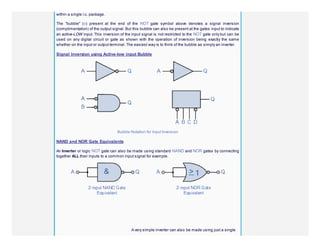
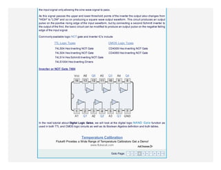


The document provides an overview of the digital logic NOT gate: - It is a single input gate that inverts its input signal, outputting a 0 when the input is 1 and vice versa. - NOT gates can be constructed using transistors or with NAND and NOR gates connected in a specific configuration. - The symbol for a NOT gate is a triangle pointing right with a circle "inversion bubble" at the output. - Common integrated circuit implementations of NOT gates include the 7404 and CD4009.