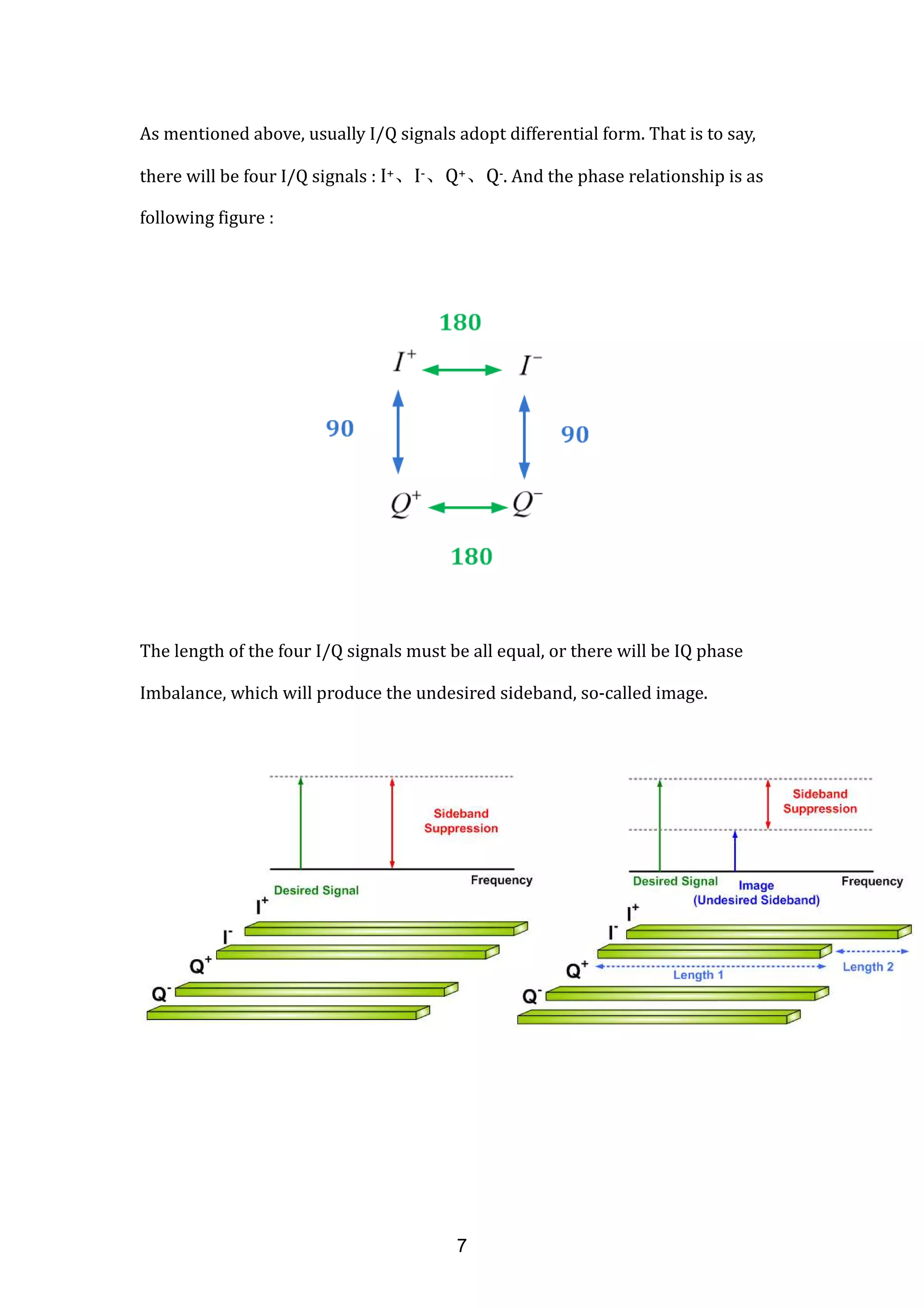
Downloaded 92 times
![Introduction
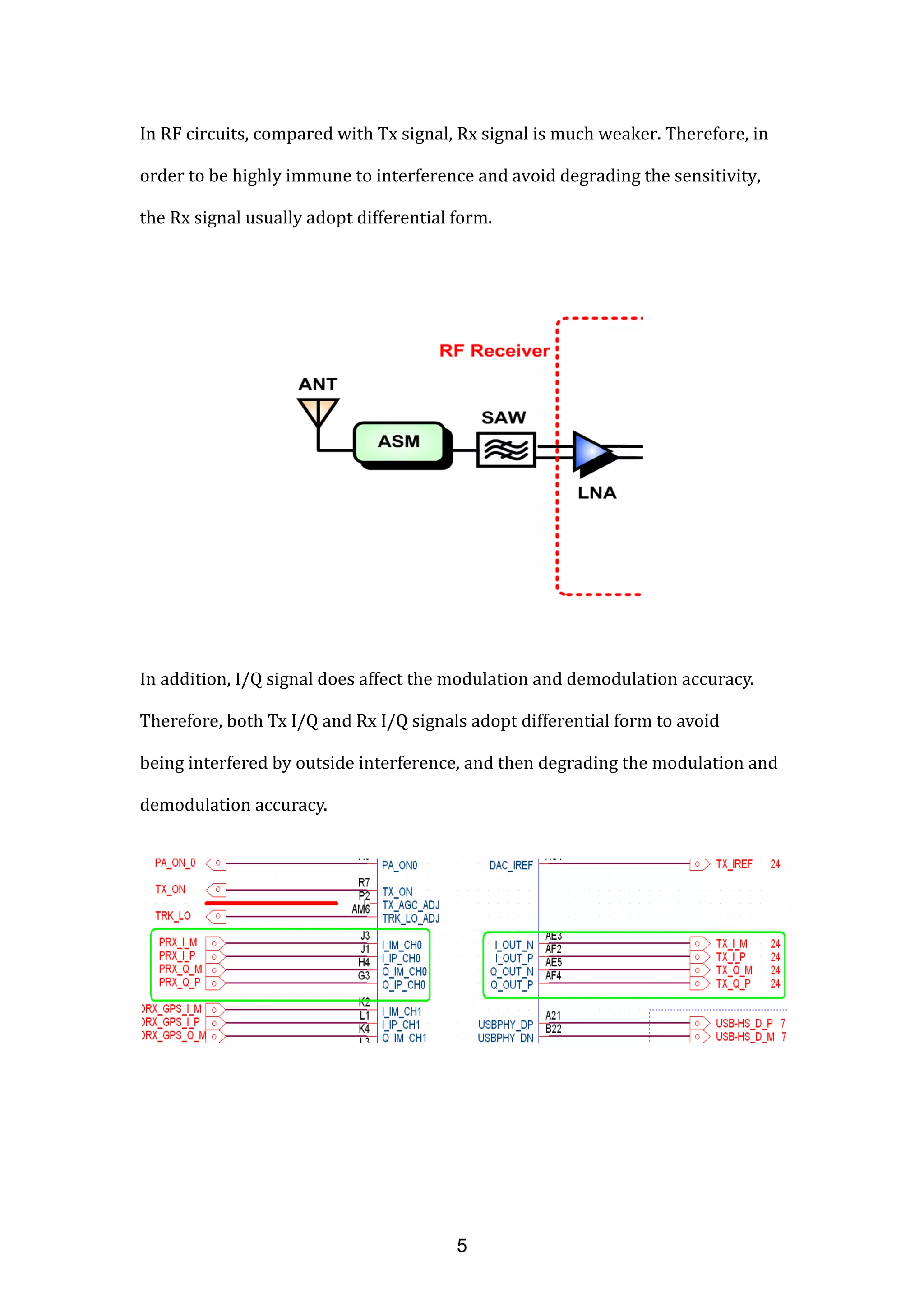
A pair of traces (wires) between the driver and receiver, one trace carries the
positive signal and the other carries a negative signal that is both equal to, and
the opposite polarity from. This is just so-called differential signal [1].
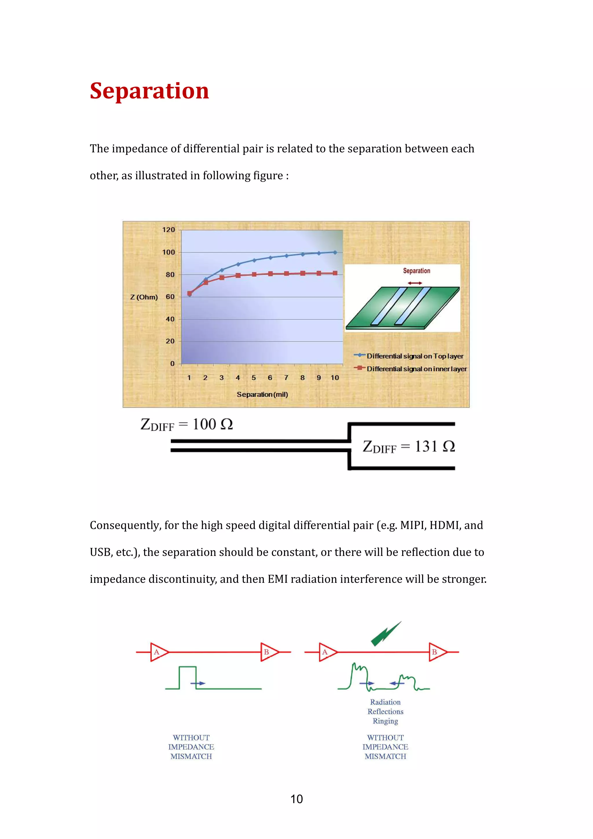
The real PCB differential trace :
1](https://image.slidesharecdn.com/introductiontodifferentialsignal-forrfandemcengineer-150912084730-lva1-app6892/75/Introduction-to-differential-signal-For-RF-and-EMC-engineer-1-2048.jpg)
![Advantage
One advantage of differential signal is with less EMI radiation. EMI radiation is
fundamentally caused by any electrical transitions with sharp edges, which
produces electromagnetic radiation. In digital systems, periodic clock signals are
the major cause of EMI [2].
2](https://image.slidesharecdn.com/introductiontodifferentialsignal-forrfandemcengineer-150912084730-lva1-app6892/75/Introduction-to-differential-signal-For-RF-and-EMC-engineer-2-2048.jpg)
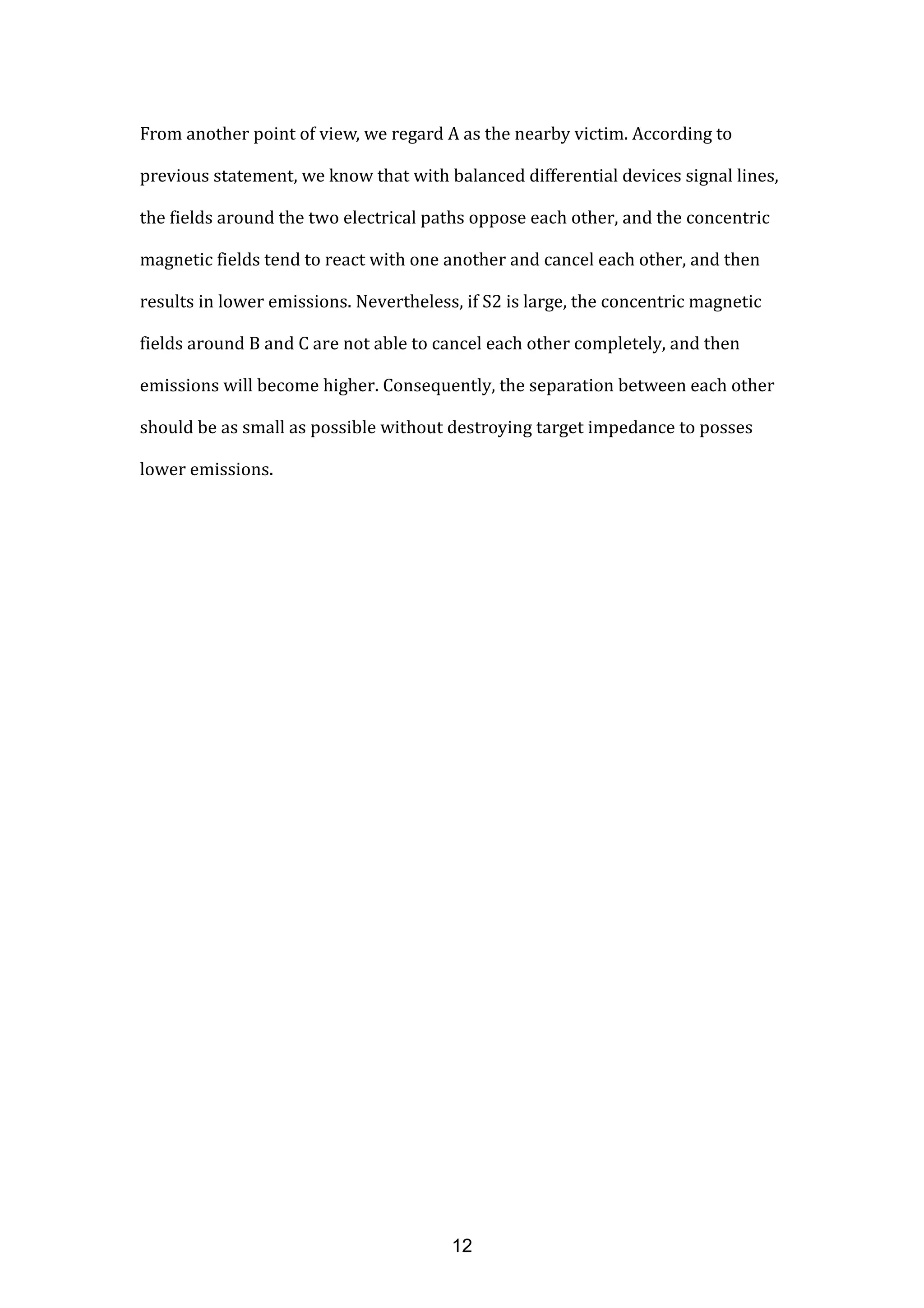
![But, with balanced differential devices signal lines, the fields around the two
electrical paths oppose each other, and the concentric magnetic fields tend to
react with one another and cancel each other, and then results in lower
emissions [2-3].
This is the reason why usually high speed digital signals are differential form.
3](https://image.slidesharecdn.com/introductiontodifferentialsignal-forrfandemcengineer-150912084730-lva1-app6892/75/Introduction-to-differential-signal-For-RF-and-EMC-engineer-3-2048.jpg)
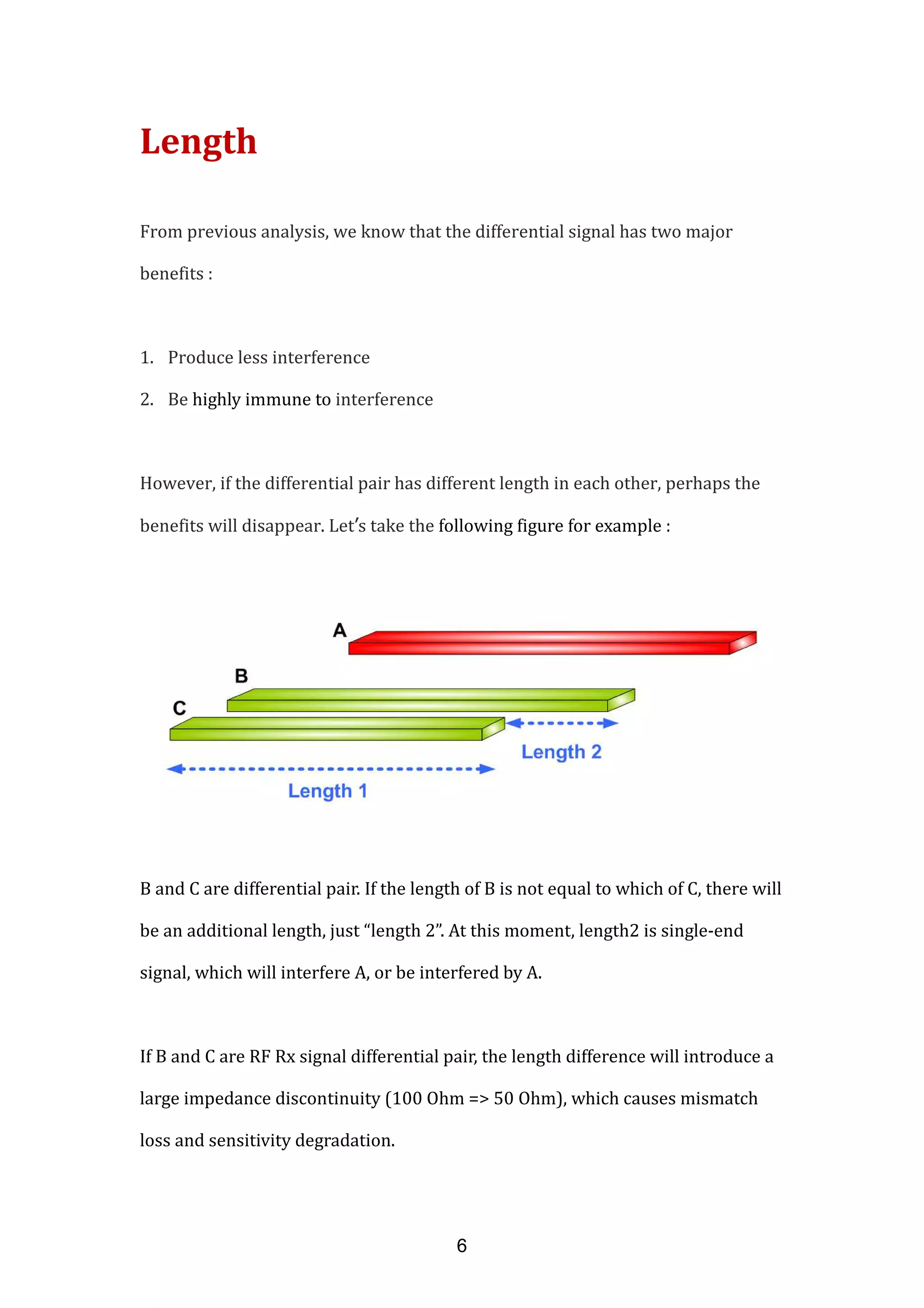
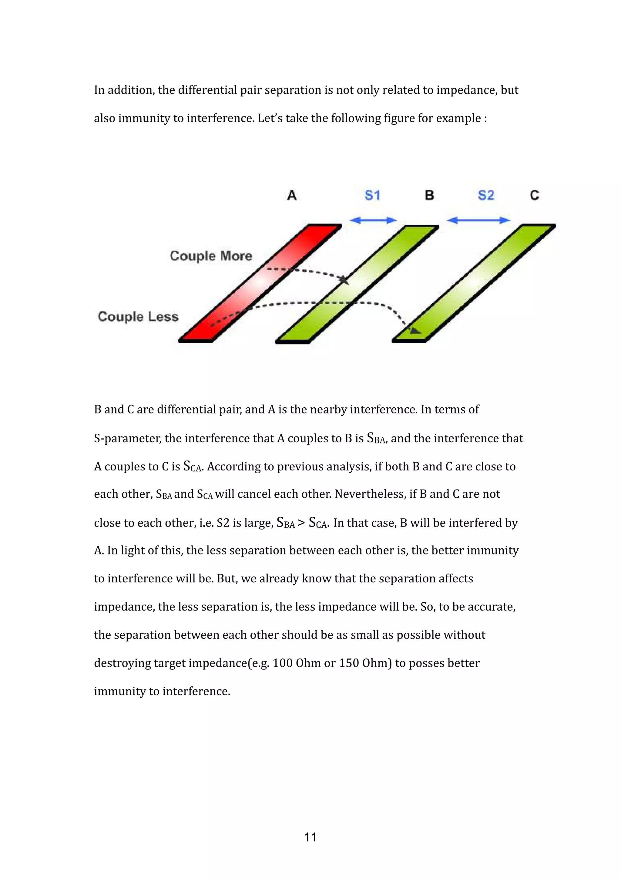
![The second major benefit of differential signaling is that it is highly immune to
outside electromagnetic interference(EMI) and crosstalk from nearby signal
conductors. An example of how it works is shown in following figure [4] :
B and C are differential pair, and A is the nearby interference. In terms of
S-parameter, the interference that A couples to B is SBA, and the interference that
A couples to C is SCA. If both B and C are close to each other, SBA and SCA will be
roughly equal. Besides, B and C have opposite direction on signal propagating.
That is to say, SBA and SCA will be roughly equal and opposite, and then cancel
each other. It’s the reason why that differential signaling is highly immune to
outside interference.
4](https://image.slidesharecdn.com/introductiontodifferentialsignal-forrfandemcengineer-150912084730-lva1-app6892/75/Introduction-to-differential-signal-For-RF-and-EMC-engineer-4-2048.jpg)
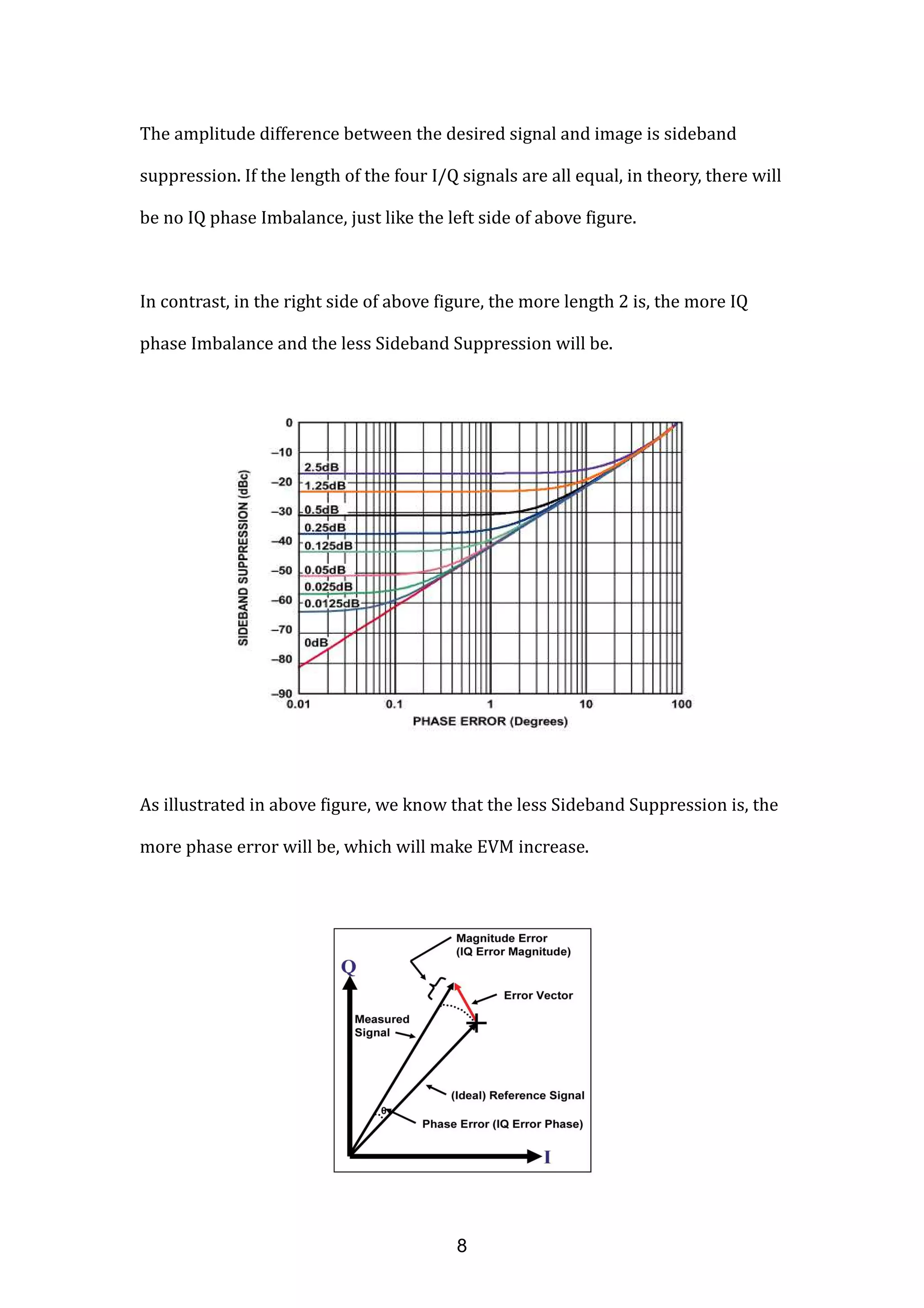
![According to [5], we know that SNR is inversely proportional to EVM :
That is to say, in terms of Rx I/Q differential signal, the more length difference is,
the more EVM, the less SNR, and the poorer sensitivity will be.
9](https://image.slidesharecdn.com/introductiontodifferentialsignal-forrfandemcengineer-150912084730-lva1-app6892/75/Introduction-to-differential-signal-For-RF-and-EMC-engineer-9-2048.jpg)
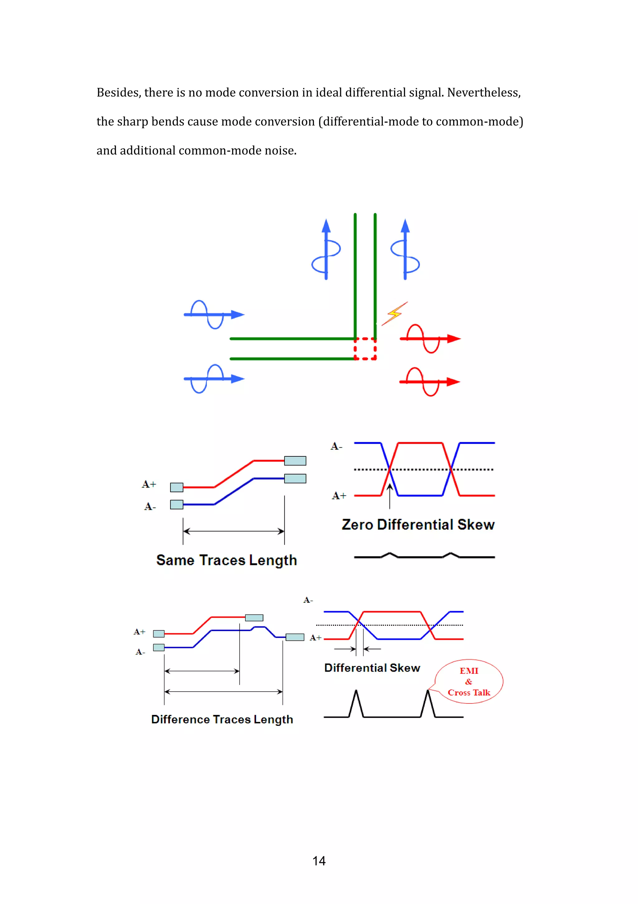
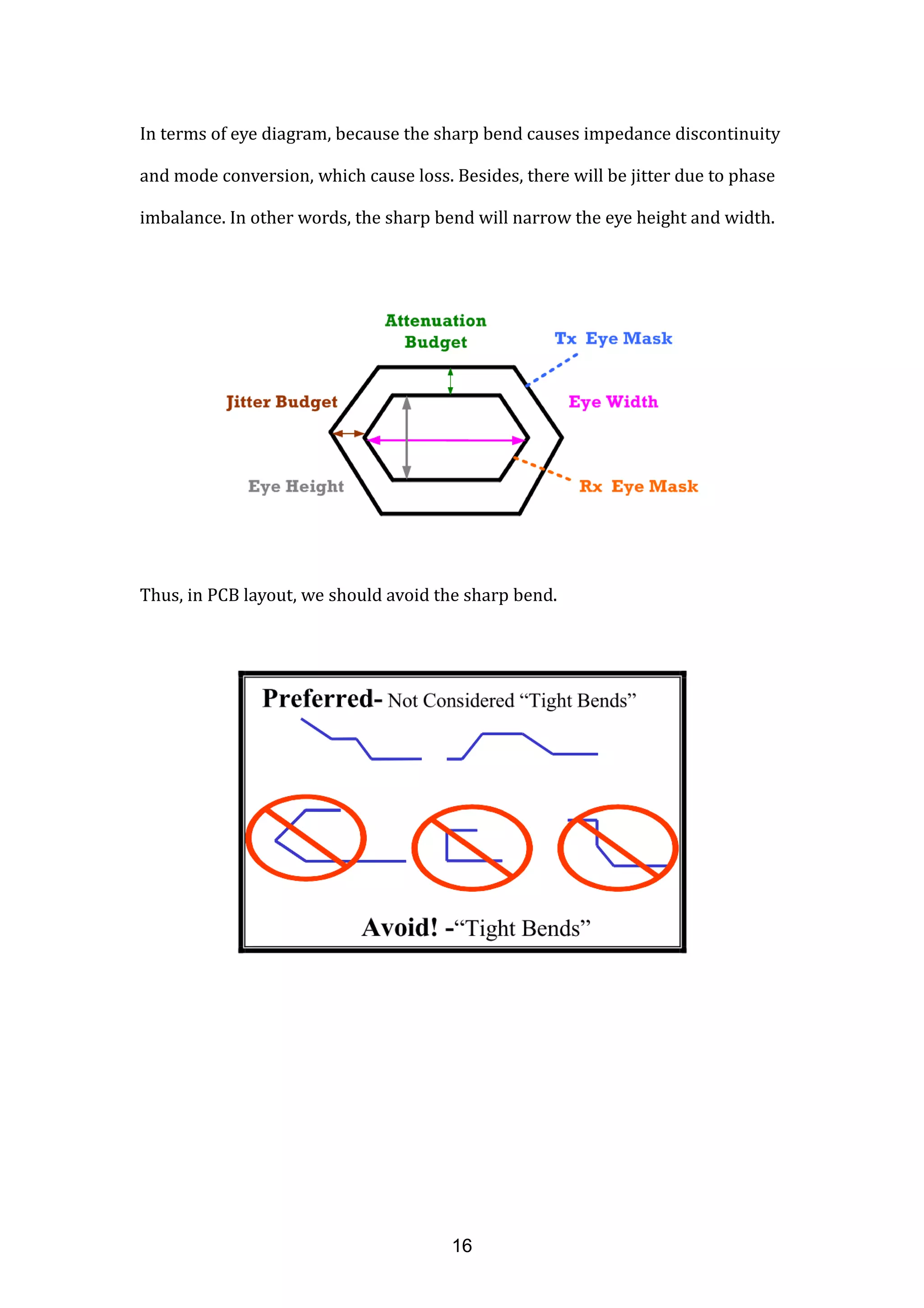
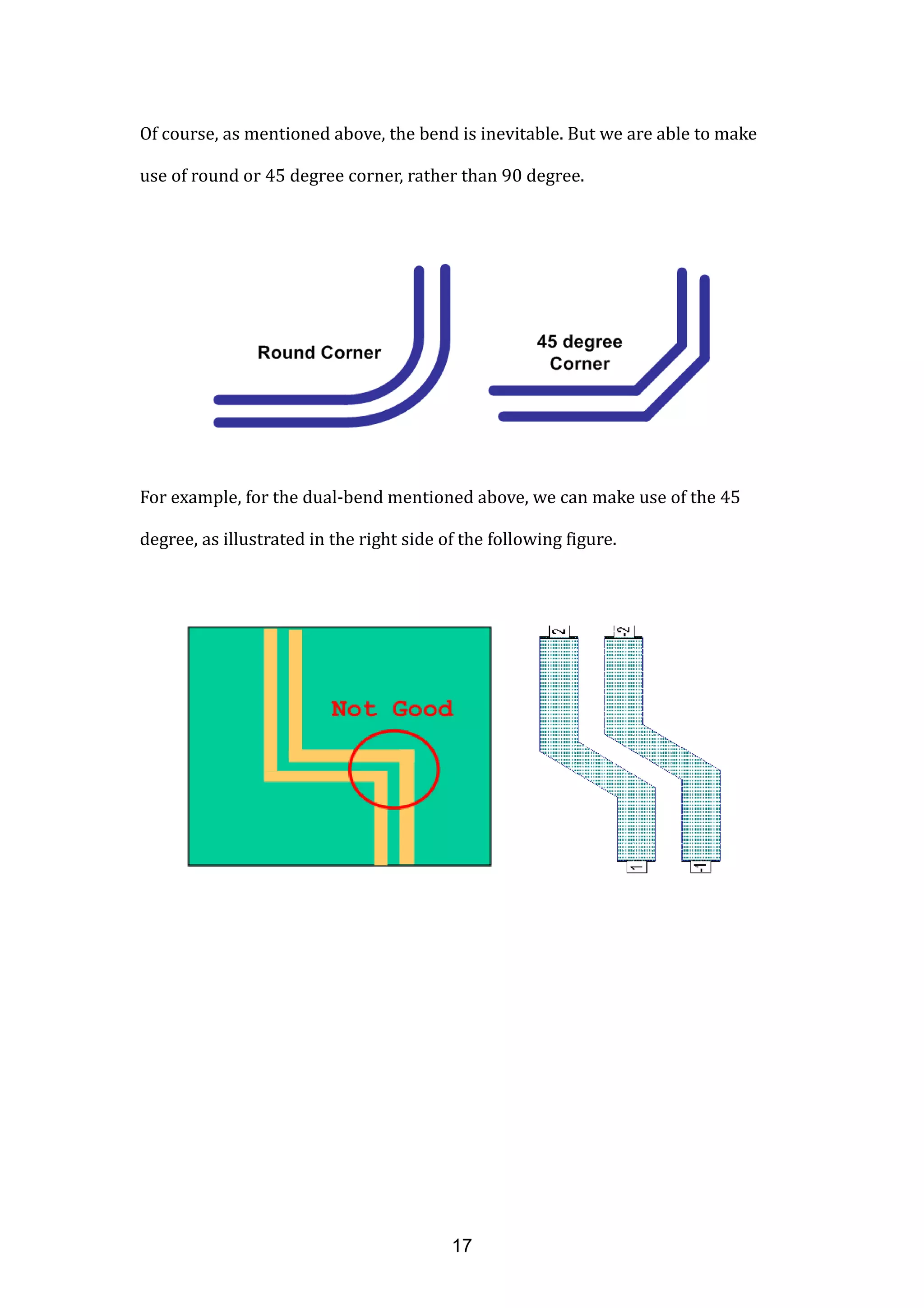
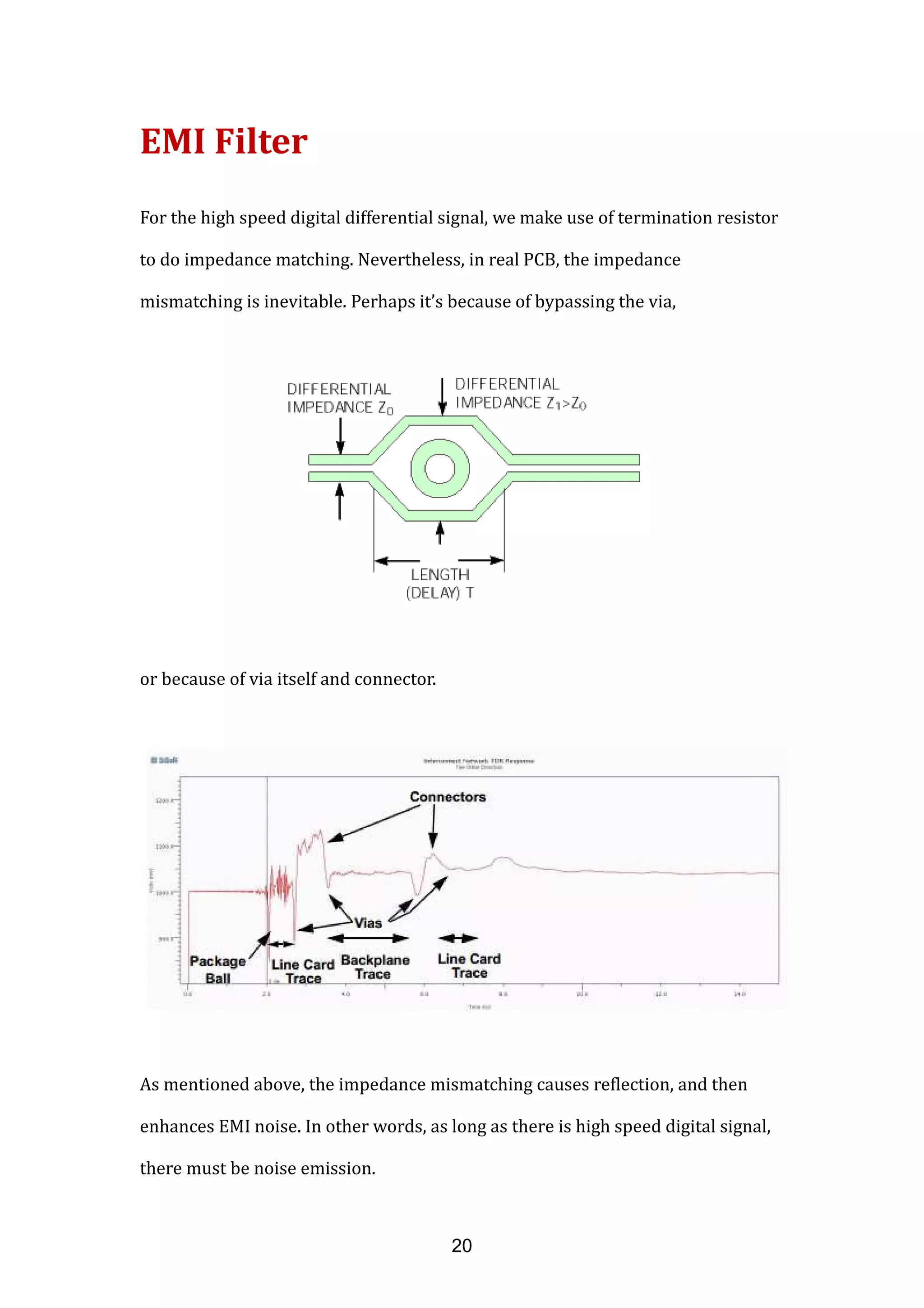
![Bend
In real PCB, it’s impossible for the differential traces to be only straight. The bend
is inevitable, and then causes extra length and additional common-mode noise.
Consequently, the conventional method is to bend again to compensate for the
length difference.
But, as shown in the above figure, these bends are all bad. Because these bends
are all sharp, i.e. 90 degree, which causes impedance discontinuity and signal
reflection [6].
13](https://image.slidesharecdn.com/introductiontodifferentialsignal-forrfandemcengineer-150912084730-lva1-app6892/75/Introduction-to-differential-signal-For-RF-and-EMC-engineer-13-2048.jpg)
![According to [6-7], the less the rising time is , the more the common-mode noise
due to sharp bend is.
And as shown in the following figure, the more length of L is, the more the
common-mode noise due to sharp bend is.
15](https://image.slidesharecdn.com/introductiontodifferentialsignal-forrfandemcengineer-150912084730-lva1-app6892/75/Introduction-to-differential-signal-For-RF-and-EMC-engineer-15-2048.jpg)
![According to [8], the ranking of phase imbalance due to bend :
90 degree > 45 degree > round corner
And the common-mode noise due to round corner is actually smaller than 90
degree.
18](https://image.slidesharecdn.com/introductiontodifferentialsignal-forrfandemcengineer-150912084730-lva1-app6892/75/Introduction-to-differential-signal-For-RF-and-EMC-engineer-18-2048.jpg)
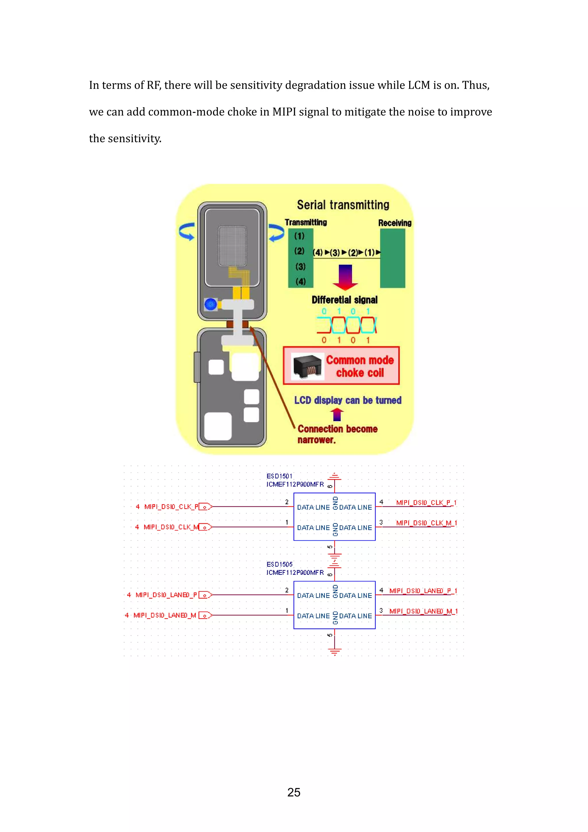
![For example, MDDI or MIPI may radiate noise to RF antenna, and then sensitivity
degrades [10].
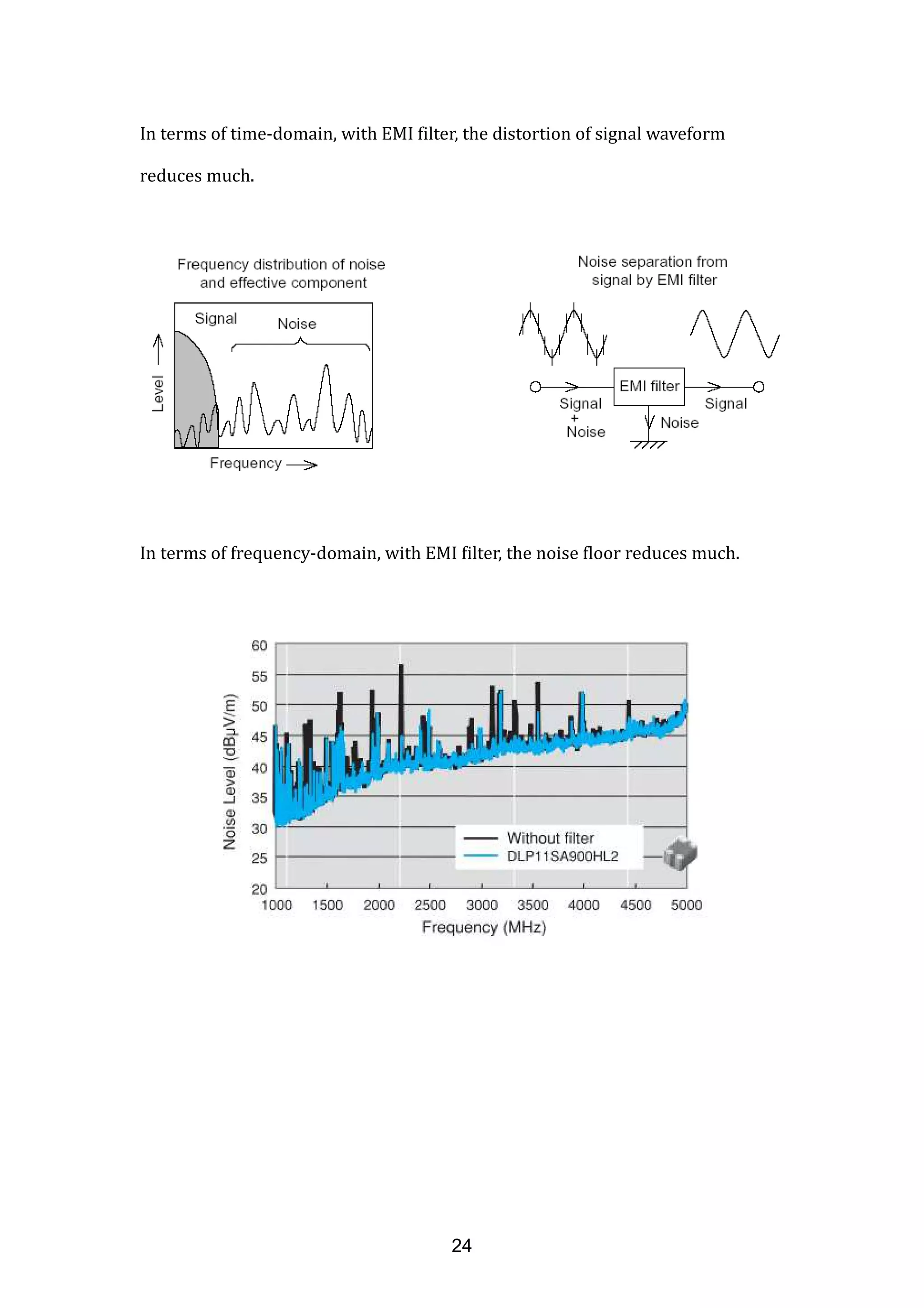
In terms of time-domain, the noise will distort the signal waveform.
Thus, we need to suppress the noise due to high speed digital signal. The most
common method is to make use of EMI filter.
21](https://image.slidesharecdn.com/introductiontodifferentialsignal-forrfandemcengineer-150912084730-lva1-app6892/75/Introduction-to-differential-signal-For-RF-and-EMC-engineer-21-2048.jpg)
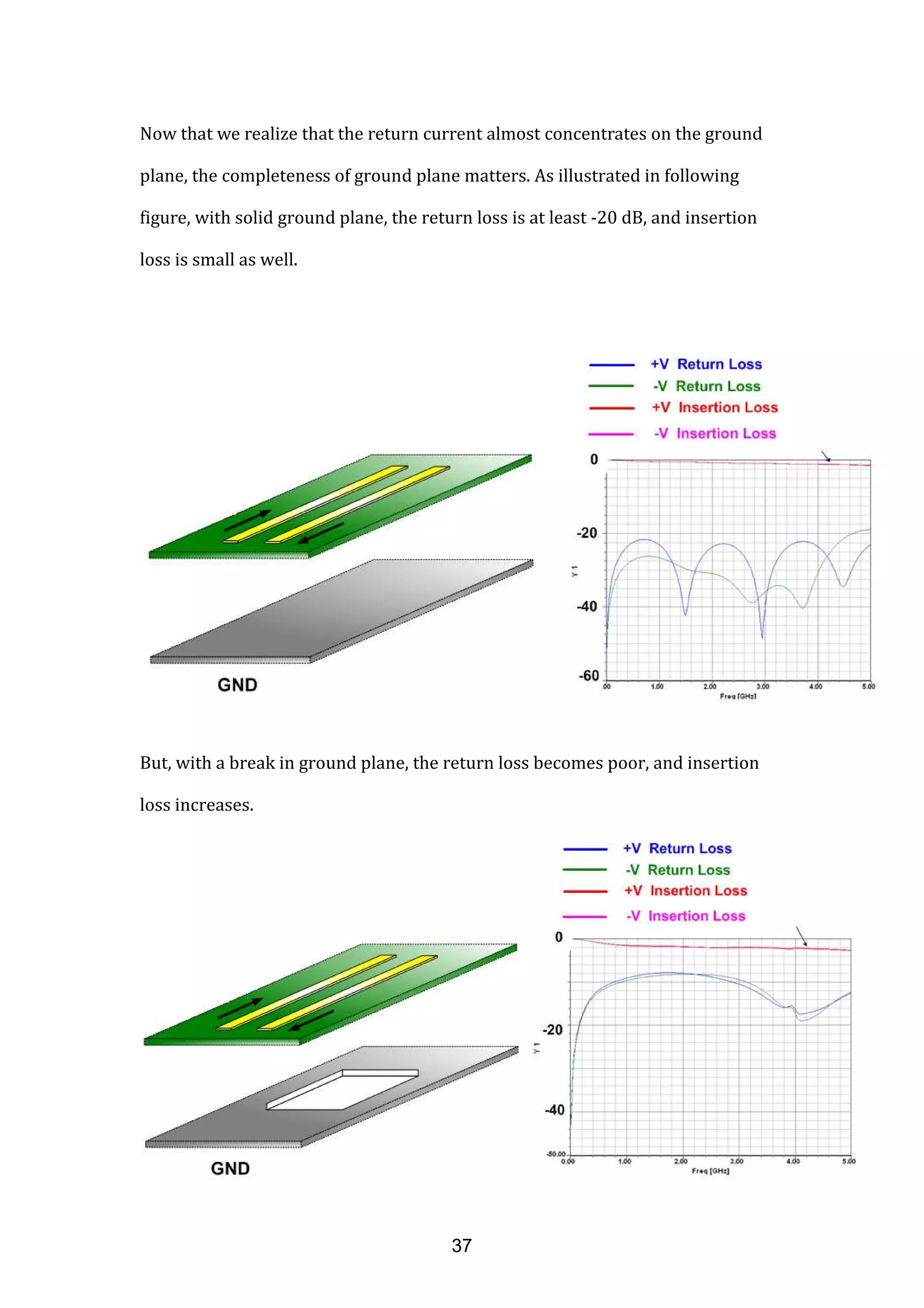
![Ground
According to [11], all currents return to their source. In other words, currents
flow in loops.
As illustrated in the following figure and formulas, we know that the larger the
loop area is, the larger the inductance is and vice versa.
30](https://image.slidesharecdn.com/introductiontodifferentialsignal-forrfandemcengineer-150912084730-lva1-app6892/75/Introduction-to-differential-signal-For-RF-and-EMC-engineer-30-2048.jpg)
![According to [12], current will always follows the path with least impedance. At
low frequency, the resistance of a path dominates the impedance, while at high
frequency, the inductance of a path dominates. This is best summarized as
follows:
– Low frequency current flows through the path with least resistance.
– High frequency current flows through the path with least inductance
As mentioned above, the smaller the loop area is, the smaller the inductance is.
That is to say, the return current of high frequency signal follows the path with
least loop area. Therefore, as illustrated in the above figure, although the return
path of high frequency is longer than which of low frequency, the loop area of
high frequency is smaller than which of low frequency. Consequently, we realize
that the return current of high frequency is underneath the signal path.
31](https://image.slidesharecdn.com/introductiontodifferentialsignal-forrfandemcengineer-150912084730-lva1-app6892/75/Introduction-to-differential-signal-For-RF-and-EMC-engineer-31-2048.jpg)
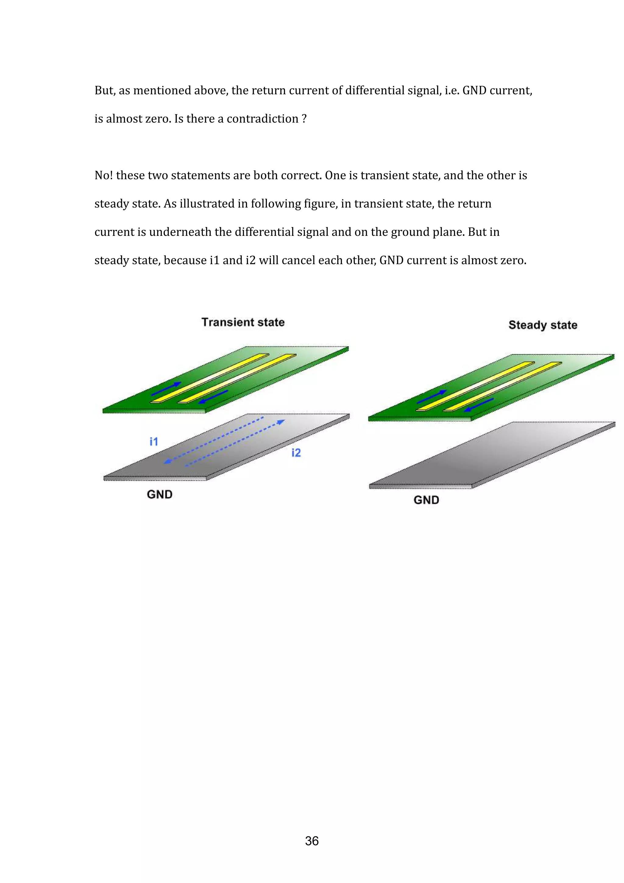
![However, as illustrated in the following figure, the return current of differential
signal, i.e. GND current, is almost zero. Thus, we wonder that does the return
current of differential signal exist in adjacent trace, not in ground ?
According to [13], we know that differential pair not only couples to ground, but
also to adjacent trace in differential-mode.
As mentioned above, the return current of high frequency signal follows the path
with least loop area. That is to say, for differential signal, the path with least loop
area is just the return path.
33](https://image.slidesharecdn.com/introductiontodifferentialsignal-forrfandemcengineer-150912084730-lva1-app6892/75/Introduction-to-differential-signal-For-RF-and-EMC-engineer-33-2048.jpg)
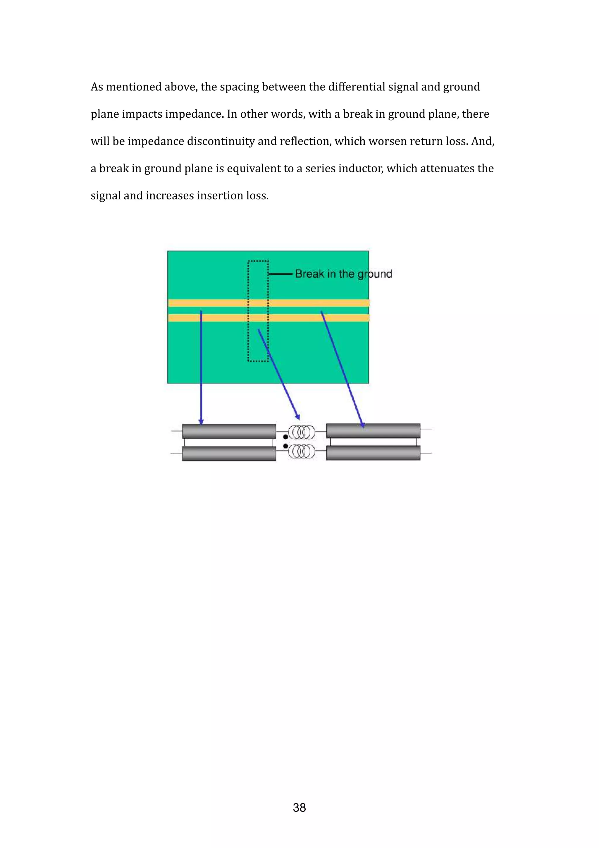
![According to [14], Ground Bounce distorts the signal waveform, affects the circuit
logic, and worsens the system stability.
As illustrated in following figure, with a break in ground plane, there will be
Ground Bounce.
Therefore, the ground plane should be as solid as possible.
39](https://image.slidesharecdn.com/introductiontodifferentialsignal-forrfandemcengineer-150912084730-lva1-app6892/75/Introduction-to-differential-signal-For-RF-and-EMC-engineer-39-2048.jpg)
![Although in steady state, the ground current is almost zero. Nevertheless, due to
crosstalk, there will still be an induced current flowing in a closed loop on the
ground plane under the differential pair, and produces noise emission [1].
According to [15], the 3W rule can further minimize 70% crosstalk. So, should
we increase the spacing between the differential pair and the ground plane to
reduce the induced current ?
40](https://image.slidesharecdn.com/introductiontodifferentialsignal-forrfandemcengineer-150912084730-lva1-app6892/75/Introduction-to-differential-signal-For-RF-and-EMC-engineer-40-2048.jpg)
![No! you can’t increase the spacing. Because in real PCB, the length of differential
pair is hardly equal. That is to say, more or less, there must be an extra length,
which is single-end signal with return path on the ground plane. Thus, the more
spacing is, the larger the loop area of single-end signal is. Undoubtedly, large
loop area causes strong noise emission.
According to[1], the loop area of induced current is the same as which of
differential pair. And as mentioned above, in real PCB, the return current almost
concentrates on the ground plane. In other words, instead of increasing the
spacing, you should decrease the spacing to minimize the loop area of induced
current and differential pair. Besides, for loop area reduction, you should shorten
the length of differential pair, and decrease the spacing between each other of the
differential pair (without affecting target impedance) as well.
41](https://image.slidesharecdn.com/introductiontodifferentialsignal-forrfandemcengineer-150912084730-lva1-app6892/75/Introduction-to-differential-signal-For-RF-and-EMC-engineer-41-2048.jpg)
![Reference
[1] Differential Signals:Rules to Live By
[2] LVDS Reduces EMI, FAIRCHILD
[3] Design For EMI, INTEL
[4] What is a Differential Signal? Lattice
[5] On the Extended Relationships Among EVM, BER and SNR as Performance
Metrics
[6] Signal Integrity Issues for High-Speed Serial Differential Interconnects
[7] INTERCONNECT SIGNAL INTEGRITY, SAMTEC
[8] Your layout is skewed
[9] Breaking Up A Pair
[10] EMI countermeasure for Smartphone, TAIYO YUDEN
[11] Emc & the Printed Circuit Board: Design, Theory, & Layout Made Simple
[12] Part 4 –PCB LAYOUT RULES FOR SIGNAL INTEGRITY
[13] The Truth about Differential Pairs in High Speed PCBs
[14] Understanding and Minimizing Ground Bounce, FAIRCHILD
[15] Designing for Board Level Electromagnetic Compatibility
44](https://image.slidesharecdn.com/introductiontodifferentialsignal-forrfandemcengineer-150912084730-lva1-app6892/75/Introduction-to-differential-signal-For-RF-and-EMC-engineer-44-2048.jpg)

The document discusses design considerations for differential signaling on PCBs. It notes that differential signaling has advantages of producing less electromagnetic interference and being highly immune to interference. However, it also notes that differences in length or spacing between differential pair traces can reduce these advantages. Specifically, the key points are that the length of each trace in a differential pair should be equal, the spacing between traces should be constant, and bends should be gradual rather than sharp to avoid impedance discontinuities and mode conversion that degrade signal quality and increase noise.