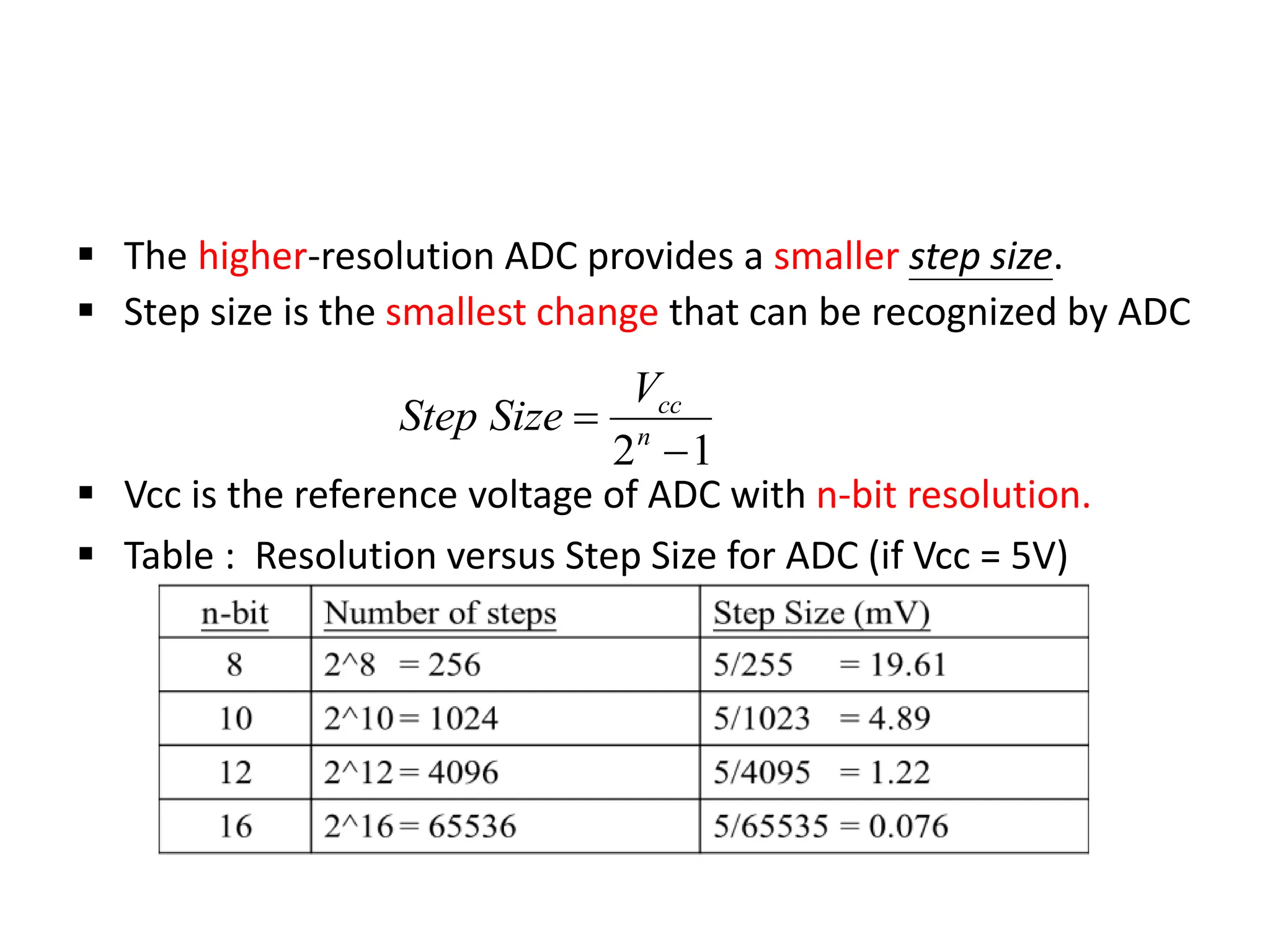
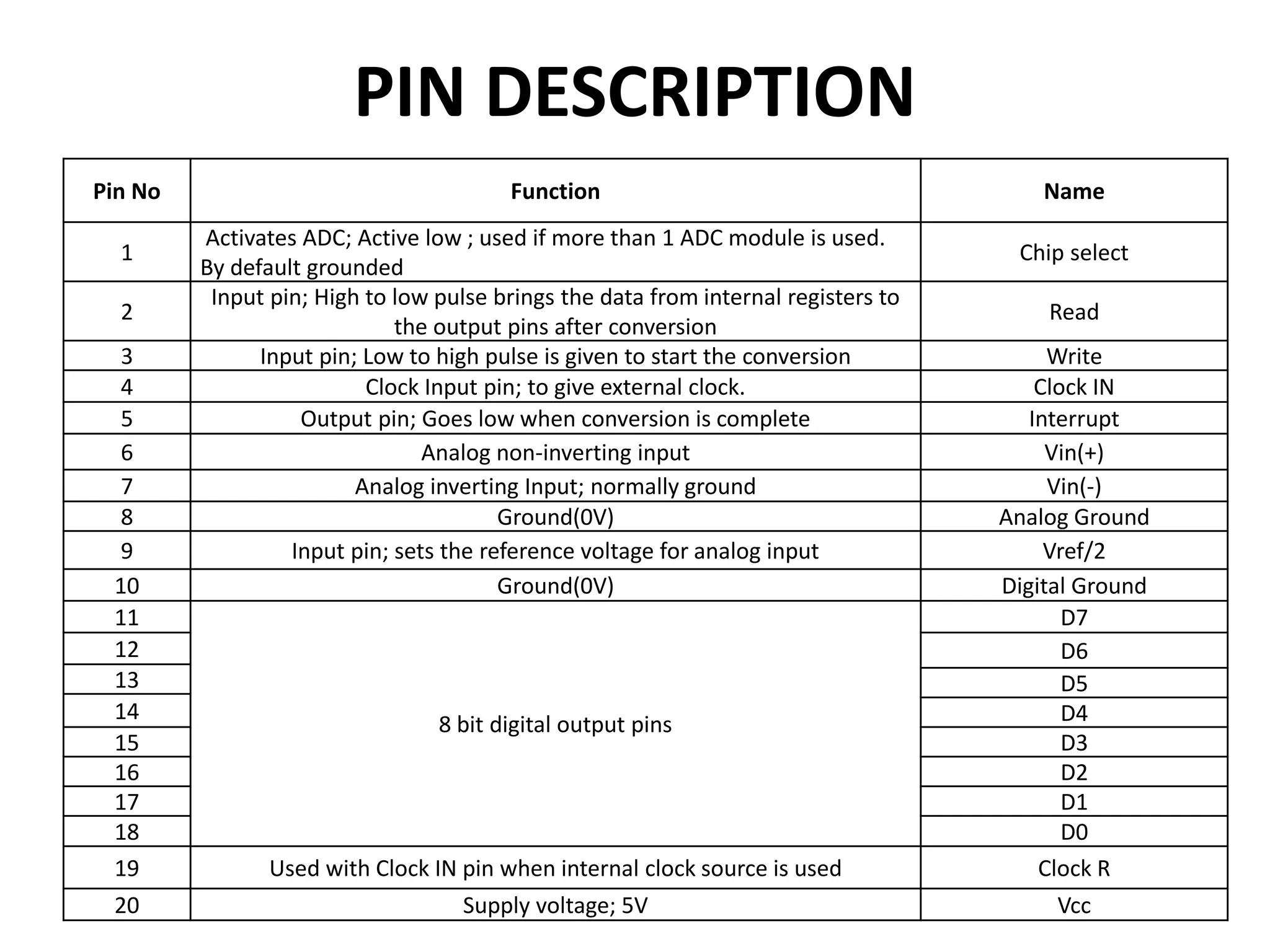
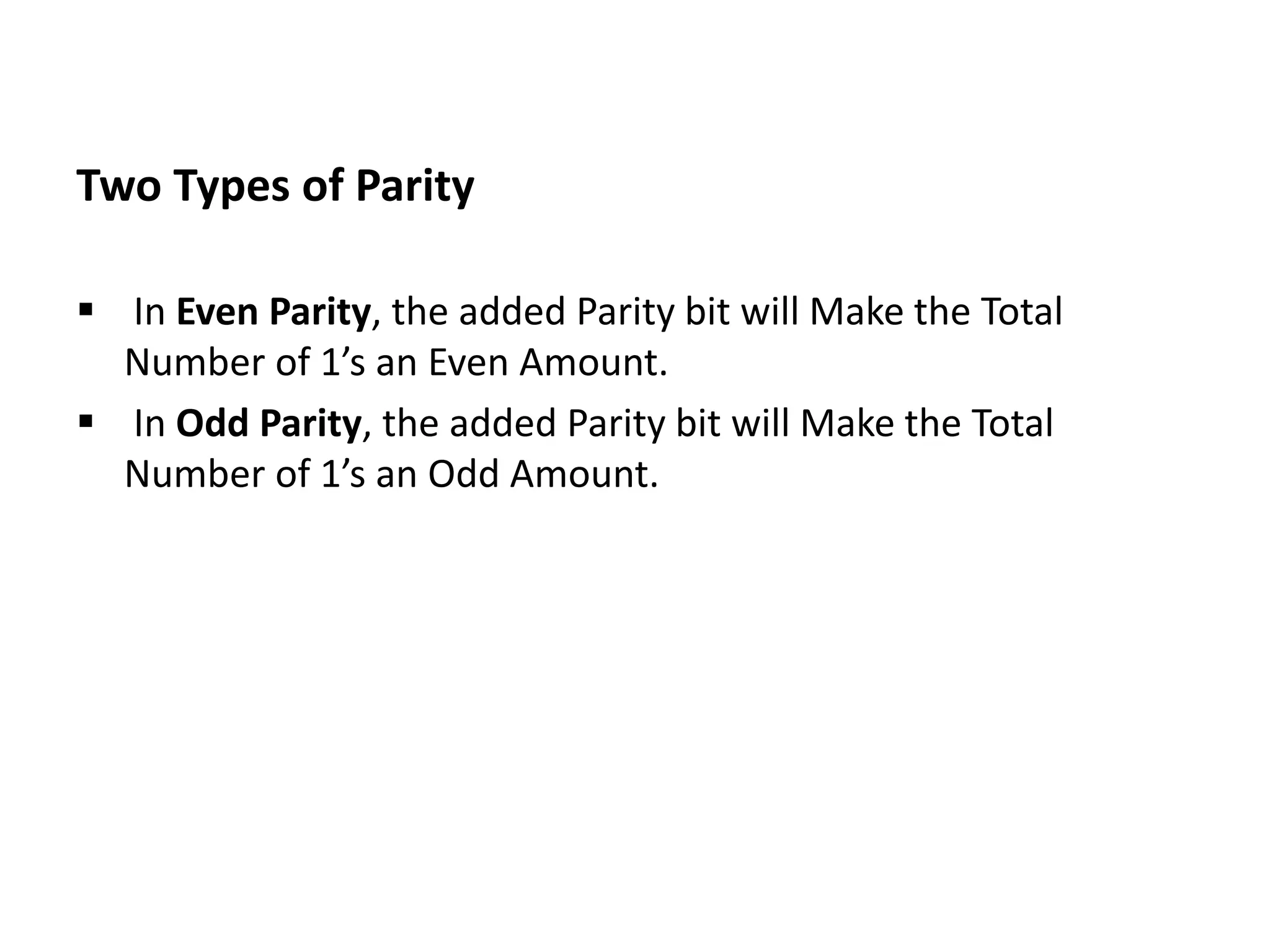
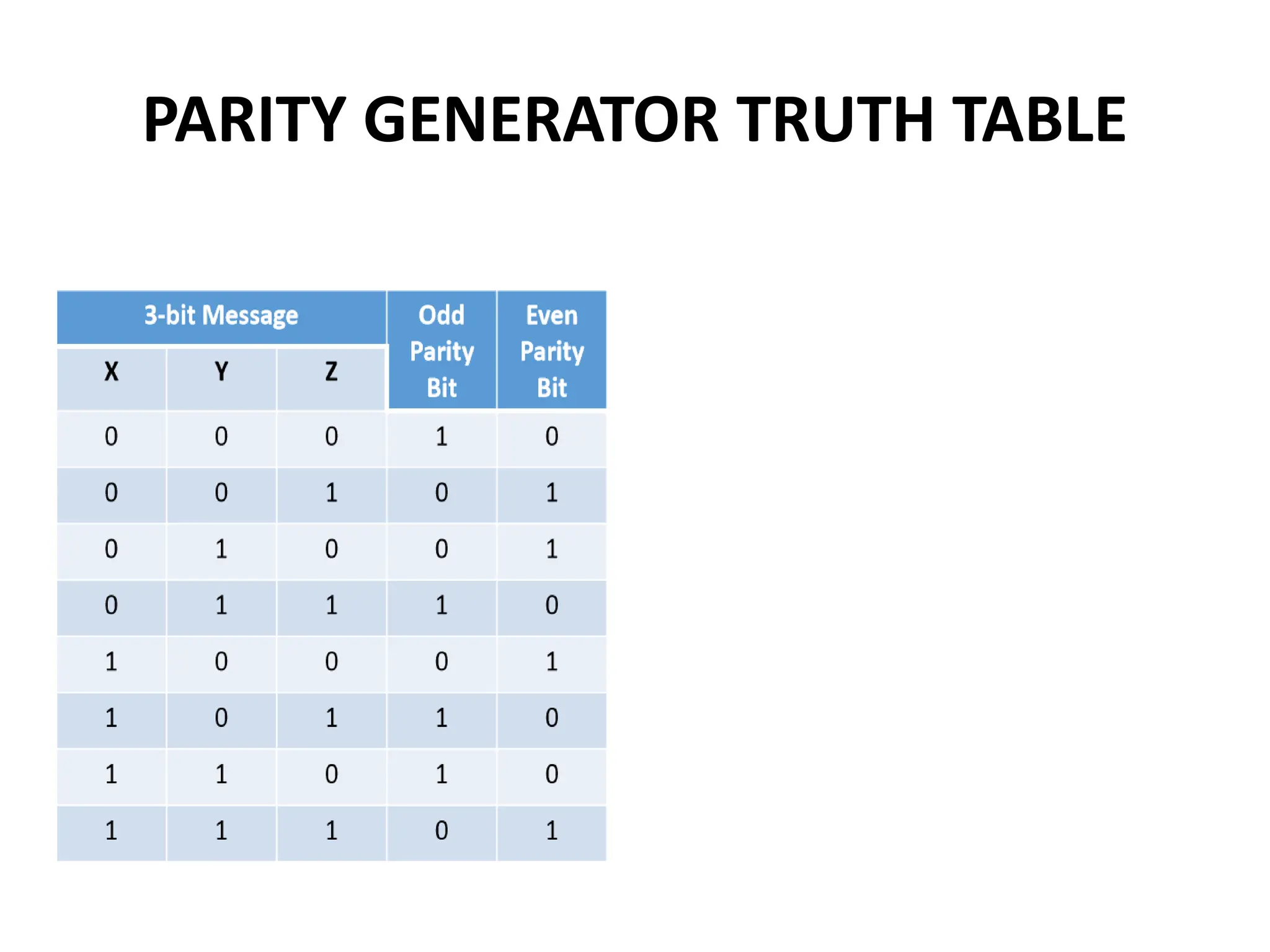
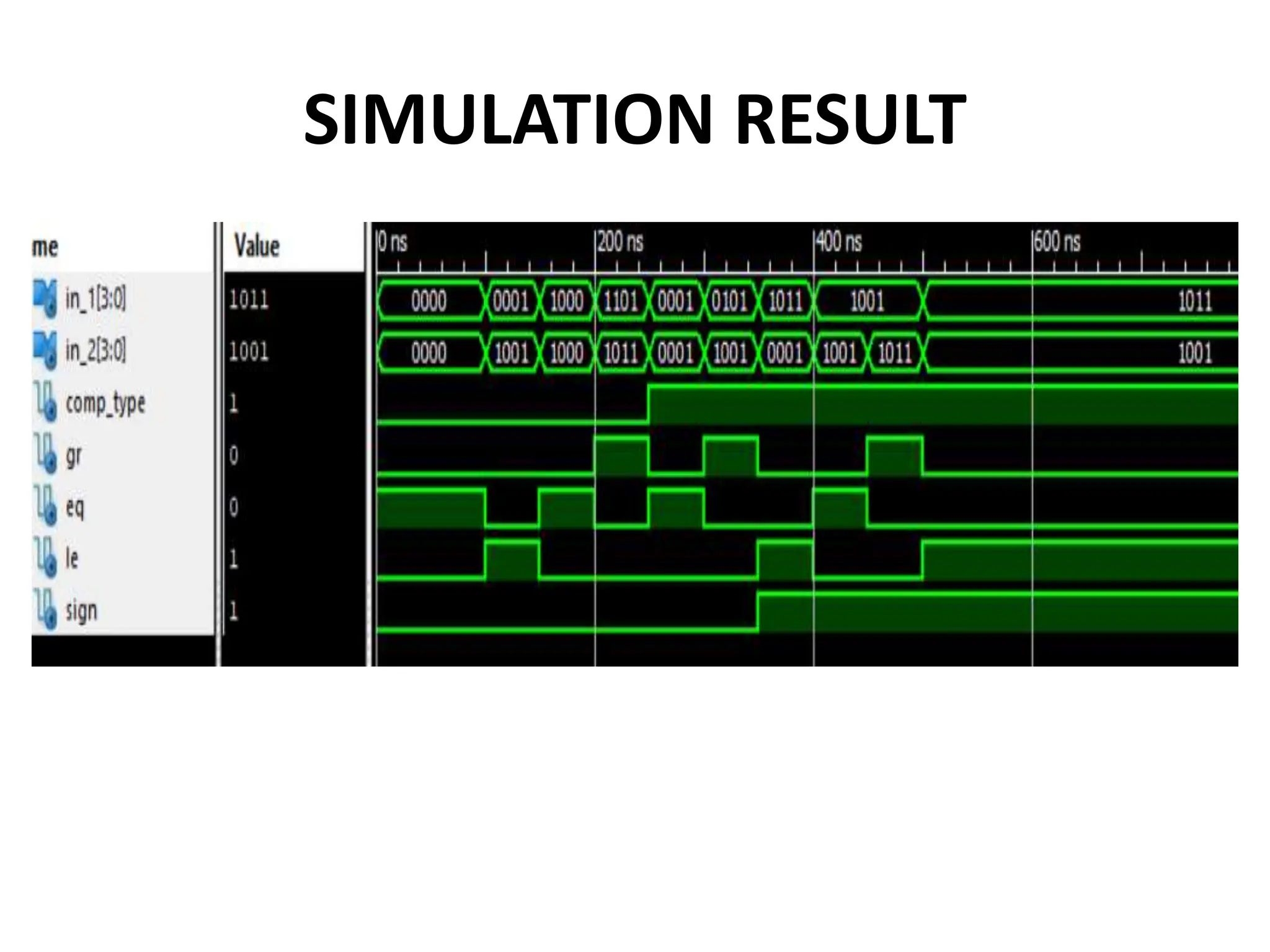
3. ADC
Analog-to-digital converter (ADC) is a device which can
convert analogue voltage to digital numbers so that
microcontrollers and microprocessors can handle and process
the data.
ADC are the most widely used devices for data acquisition.
ADC has n-bit resolution, where n can be 8, 12, 16 or even 24
bits.
4. The higher-resolution ADC provides a smaller step size.
Step size is the smallest change that can be recognized by ADC
Vcc is the reference voltage of ADC with n-bit resolution.
Table : Resolution versus Step Size for ADC (if Vcc = 5V)
1
2
n
cc
V
Size
Step
6. ADC0804
Features
Single channel ,8-bit parallel ADC module
Easy to interface with all
Microprocessors or works
Stand alone.
Differential analog voltage inputs. 0V to 5V analog input
voltage range with single 5V supply.
On chip Clock available.
7. Digital output various from 0 to 255.
When Vref = 5V, for every 19.60mV of analog value there will
be rise of one bit on digital side (Step size)
Available in 20-pin PDIP, SOIC packages.
A common, low-cost ADC, compatible with a wide range of
microprocessors. There are many faster ADCs available with
more resolution, this device is ideal for applications that do
not require a high degree of accuracy.
ADC0804 requires up to 100 µs to convert an analog input
voltage into a digital output code.
9. PIN DESCRIPTION
Pin No Function Name
1
Activates ADC; Active low ; used if more than 1 ADC module is used.
By default grounded
Chip select
2
Input pin; High to low pulse brings the data from internal registers to
the output pins after conversion
Read
3 Input pin; Low to high pulse is given to start the conversion Write
4 Clock Input pin; to give external clock. Clock IN
5 Output pin; Goes low when conversion is complete Interrupt
6 Analog non-inverting input Vin(+)
7 Analog inverting Input; normally ground Vin(-)
8 Ground(0V) Analog Ground
9 Input pin; sets the reference voltage for analog input Vref/2
10 Ground(0V) Digital Ground
11
8 bit digital output pins
D7
12 D6
13 D5
14 D4
15 D3
16 D2
17 D1
18 D0
19 Used with Clock IN pin when internal clock source is used Clock R
20 Supply voltage; 5V Vcc
16. PARITY GENERATOR
A Parity Generator is a Combinational Logic Circuit that
Generates the Parity bit in the Transmitter.
A Parity bit is used for the Purpose of Detecting Errors during
Transmissions of binary Information.
It is an Extra bit Included with a binary Message to Make the
Number of 1’s either Odd or Even.
17. Two Types of Parity
In Even Parity, the added Parity bit will Make the Total
Number of 1’s an Even Amount.
In Odd Parity, the added Parity bit will Make the Total
Number of 1’s an Odd Amount.