SlideShare a Scribd company logo
Improving PSRR and
CMRR in Fully Differential
Amplifiers
Introduction
Power Supply Rejection Ratio (PSRR) and Common Mode
Rejection Ratio (CMRR) are the two key specifications when
it comes to characterizing and designing differential amplifi-
ers. Although these amplifiers are designed to give best
PSRR and CMRR performance, a careless application de-
sign and a poor selection of external components can sig-
nificantly affect these specifications and degrade the overall
performance. In this application note, we will look at some of
the effects that external components have on PSRR and
CMRR: mismatched external gain-setting resistors, the role
of the bypass capacitor on PSRR, and some layout tech-
niques that improve CMRR and PSRR.
In Figure 1, a typical fully differential amplifier block diagram
is shown with external gain resistors and an optional bias
generator bypass capacitor. DC outputs at Vo1 and Vo2 are
biased to half-VDD by internal bias circuitry. AC signals at
Vo1 and Vo2 are 180˚ out of phase with respect to each
other, creating a Bridge-Tied-Load (BTL) configuration.
These amplifiers run with minimal component count, reduc-
ing layout time and system cost. Care must be taken to
achieve the best possible performance from these
amplifiers.
20182501
FIGURE 1. Fully Differential Amplifier Block Diagram
National Semiconductor
Application Note 1447
Kashif Javaid
July 2006
Improving
PSRR
and
CMRR
in
Fully
Differential
Amplifiers
AN-1447
© 2006 National Semiconductor Corporation AN201825 www.national.com
Application Information
MEASURING POWER SUPPLY REJECTION RATIO
(PSRR)
The type of PSRR we are interested in here is an AC
specification measuring the ability of the amplifier to reject
AC-ripple voltage on the power supply bus, as opposed to a
DC specification where we measure the change in output
voltage for a change in supply voltage. Basically, ripple
PSRR is the ratio of the differential output voltage to the
supply ripple voltage expressed in dB as shown in Equation
1.
(1)
A test circuit for measuring PSRR is shown in Figure 2. The
amplifier’s AC inputs are terminated to GND with a low value
resistor—typically 10Ω. The value of the input capacitors
Ci1 and Ci2 should be matched as closely as possible. Any
mismatch can compromise PSRR performance at low fre-
quencies. An alternate solution is the elimination of input
coupling capacitors terminating the inputs directly to GND. A
low-level AC voltage, in the range of 100mVpp to 500mVpp
is combined with VDD. This AC plus DC signal is applied to
the amplifier’s VDD pin. Any residual AC signal at the ripple
frequency present across the BTL outputs is a function of the
amplifier’s PSRR. The magnitude of this residual signal is
measured with an FFT (using a spectrum analyzer or Audio
Precision instrument). Using Equation 1 gives the PSRR
value in dB.
MEASURING COMMON MODE REJECTION RATIO
(CMRR)
Common Mode Rejection Ratio is an ability of the differential
amplifier to reject common mode input signal and is ex-
pressed in dB as shown in Equation 2.
(2)
A test circuit for measuring CMRR is shown is Figure 3. The
amplifier’s AC inputs are connected to a common-mode AC
input. Output can be measured by using a high precision AC
Volt Meter or Audio Precision instrument. Equation 2 gives
the CMRR measurement in dB. For differential input ampli-
fiers with external gain-settings resistors, CMRR measure-
ment is highly dependent on external resistors as well as
board layout. This will be fully discussed in the next section.
As a side note, a lot of newer audio measuring instruments
such as Audio Precision can perform the CMRR test (and a
lot of other audio parameters as well) automatically.
20182533
FIGURE 2. PSRR Measurement Test Circuit
AN-1447
www.national.com 2
Application Information (Continued)
EFFECTS OF EXTERNAL GAIN RESISTORS
It is extremely important to match the input resistors to each
other as well as the feedback resistors to each other for best
CMRR performance. When the inputs of the fully differential
amplifier are DC-coupled, resistor matching differences gen-
erate net DC currents across the load because of the bal-
anced nature of the differential amplifiers.
Internally these amplifiers consist of two circuits: a differen-
tial amplifier and a common-mode feedback amplifier that
adjusts the output voltages so that the nominal DC output
bias remains VDD/2. Assuming that the amplifier’ has two
equal “halves.” Equation 3 can be obtained by the simple
analysis of the differential amplifier in Figure 1 with Vcmi =
0V. Each half uses an input and feedback resistor (Ri and Rf)
and contributes to each side of the equation. This equation
shows an output offset DC voltage that can result because of
resistor mismatching either between feedback resistors (Rf1
and Rf2) or input resistors (Ri1 and Ri2).
(3)
Ideally, when Ri1 = Ri2 and Rf1 = Rf2, we get perfectly
matched and balanced input and feedback resistors pairs
and no offset voltage. But if, for example, we assume:
Ri1 = Ri2 = R
Rf1 = 0.8R and Rf2 = 1.2R, with 20% tolerance in the
feedback resistors.
We will get an offset voltage of about 0.45 Volts and load
current of about 46mA assuming an 8Ω load connected
across the output. Now that’s quite a big DC offset voltage!
As a result, this reduces the battery life and could affect the
speaker performance significantly because of extra DC cur-
rent flowing through the voice coil. Common Mode Rejection
Ratio is a parameter that can be gravely affected by mis-
matched gain resistors. A graph of Common Mode Rejection
Ratio vs. feedback resistor mismatch is shown in Figure 4.
As can be seen in the graph, a feedback resistor mismatch
of 0.4 reduces the CMMR approximately 23dB from the ideal
condition perfectly matched resistor.
PSRR is also affected by the gain resistors mismatch, but
with a small capacitor on the bypass pin this effect is re-
duced extensively and yields practically no effect at all on the
power supply rejection. The effects of bypass capacitor will
be fully discussed in the next section. Thus, for all practical
purpose, resistors of 1% tolerance or even better should be
used for optimal performance and best common mode re-
jection ratio.
20182507
FIGURE 3. CMRR Measurement Test Circuit
AN-1447
www.national.com
3
Application Information (Continued)
EFFECTS OF BYPASS CAPACITOR
Fully differential amplifiers offer an “optional” bypass capaci-
tor (CB) and allow a designer to use these amplifiers with
minimal component count. Before eliminating the optional
bypass capacitor to reduce component count, one should
understand how that might affect the overall performance of
the amplifier. Internally, a common mode amplifier adjusts
the two outputs to a quiescent DC voltage equal to halve-
VDD. Any supply fluctuations cause both outputs to move in
phase. This ideally creates a net change of 0VDC differen-
tially across the outputs. Thus, a bypass capacitor is not
really required and can be considered optional. But in the
real world, these amplifiers are not perfect. Furthermore,
mismatch in the external resistors can result in unbalanced
amplifier operation. PSRR is the most important parameter
that would be affected significantly by eliminating the bypass
capacitor.
Differential input amplifiers are considered excellent low
noise and high PSRR amplifiers when compared to similar
single-ended amplifiers. As shown in Figure 5 at low ripple
frequencies, the PSRR is close to 70dB, even without a
bypass capacitor. However, using a bypass capacitor in
range of 0.1 uF to 1 uF offers a significant 20dB PSRR
improvement. Depending upon the application, PSRR of
70dB might be considered good and more than adequate for
most applications. However, in cell-phone market where an
excellent PSRR is desired, particularly at lower frequencies,
20182535
FIGURE 4. CMRR vs Feedback Resistor Mismatch
20182536
FIGURE 5. PSRR vs Ripple Frequency
AN-1447
www.national.com 4
Application Information (Continued)
adding a bypass capacitor certainly will improve the lower
frequencies power supply rejection. Furthermore, the ampli-
fier will be less sensitive to slight gain resistor value mis-
match.
LAYOUT CONSIDERATIONS
Printed circuit board layout is generally considered to be
very application specific. Nevertheless, it is possible to ob-
serve some guidelines that optimize the overall performance
of the amplifier. Fully differential amplifiers come in different
packages.
Please contact the National Semiconductor Corp. website
for package-specific applications information before attempt-
ing to start any new layout. Another important factor to
consider is star ground vs. ground plane. This is very appli-
cation and package specific. Either configuration is used
when combined with the following general suggestions:
a) Make use of symmetrical placement of components (i.e.
feedback resistors and input resistors).
b) If not using ground planes, VDD and GND traces should
be as wide as possible.
c) If a heat-sink plane is desired for exposed-DAP pack-
ages, it should be appropriately sized. Refer to the power
derating graphs in the corresponding datasheet.
d) The distance between the chip and any possible antenna
source should be as far as possible.
e) If possible, make the output traces short and equal in
length and away from the any antenna source.
f) If using a star ground, all the GNDs such as bypass
capacitor GND, supply capacitor GNDs, and any other sys-
tem ground should be directly connected to a single point on
the board, possibly at the board’s point of entry for the power
supply GND.
AN-1447
www.national.com
5
Revision Table
Rev Date Description
1.0 04/20/06 Initial release.
1.1 07/24/06 Simple text edits, then re-released the App Notes into the WEB.
National does not assume any responsibility for use of any circuitry described, no circuit patent licenses are implied and National reserves
the right at any time without notice to change said circuitry and specifications.
For the most current product information visit us at www.national.com.
LIFE SUPPORT POLICY
NATIONAL’S PRODUCTS ARE NOT AUTHORIZED FOR USE AS CRITICAL COMPONENTS IN LIFE SUPPORT DEVICES OR SYSTEMS
WITHOUT THE EXPRESS WRITTEN APPROVAL OF THE PRESIDENT AND GENERAL COUNSEL OF NATIONAL SEMICONDUCTOR
CORPORATION. As used herein:
1. Life support devices or systems are devices or systems
which, (a) are intended for surgical implant into the body, or
(b) support or sustain life, and whose failure to perform when
properly used in accordance with instructions for use
provided in the labeling, can be reasonably expected to result
in a significant injury to the user.
2. A critical component is any component of a life support
device or system whose failure to perform can be reasonably
expected to cause the failure of the life support device or
system, or to affect its safety or effectiveness.
BANNED SUBSTANCE COMPLIANCE
National Semiconductor follows the provisions of the Product Stewardship Guide for Customers (CSP-9-111C2) and Banned Substances
and Materials of Interest Specification (CSP-9-111S2) for regulatory environmental compliance. Details may be found at:
www.national.com/quality/green.
Lead free products are RoHS compliant.
National Semiconductor
Americas Customer
Support Center
Email: new.feedback@nsc.com
Tel: 1-800-272-9959
National Semiconductor
Europe Customer Support Center
Fax: +49 (0) 180-530 85 86
Email: europe.support@nsc.com
Deutsch Tel: +49 (0) 69 9508 6208
English Tel: +44 (0) 870 24 0 2171
Français Tel: +33 (0) 1 41 91 8790
National Semiconductor
Asia Pacific Customer
Support Center
Email: ap.support@nsc.com
National Semiconductor
Japan Customer Support Center
Fax: 81-3-5639-7507
Email: jpn.feedback@nsc.com
Tel: 81-3-5639-7560
www.national.com
AN-1447
Improving
PSRR
and
CMRR
in
Fully
Differential
Amplifiers

More Related Content

What's hot

STRATEGY FOR OPTIMIZED BMS SYSTEMS - 800V EV BATTERY ARCHITECTURE
STRATEGY FOR OPTIMIZED BMS SYSTEMS - 800V EV BATTERY ARCHITECTURESTRATEGY FOR OPTIMIZED BMS SYSTEMS - 800V EV BATTERY ARCHITECTURE
STRATEGY FOR OPTIMIZED BMS SYSTEMS - 800V EV BATTERY ARCHITECTURE
iQHub
 
Pass Transistor Logic
Pass Transistor LogicPass Transistor Logic
Pass Transistor LogicDiwaker Pant
 
Generator Protection Relay Setting Calculations
Generator Protection Relay Setting CalculationsGenerator Protection Relay Setting Calculations
Generator Protection Relay Setting Calculations
Power System Operation
 
Verilog codes and testbench codes for basic digital electronic circuits.
Verilog codes and testbench codes for basic digital electronic circuits. Verilog codes and testbench codes for basic digital electronic circuits.
Verilog codes and testbench codes for basic digital electronic circuits.
shobhan pujari
 
Short Circuit, Protective Device Coordination
Short Circuit, Protective Device CoordinationShort Circuit, Protective Device Coordination
Short Circuit, Protective Device Coordination
michaeljmack
 
B.Tech Project PPT on MINIATURE ACTIVE MODEL SUBSTATION
B.Tech Project PPT on MINIATURE ACTIVE MODEL SUBSTATIONB.Tech Project PPT on MINIATURE ACTIVE MODEL SUBSTATION
B.Tech Project PPT on MINIATURE ACTIVE MODEL SUBSTATION
MAINAK SINGHA BARMA
 
Power
PowerPower
Fault Level Calculation
Fault Level CalculationFault Level Calculation
Fault Level CalculationDinesh Sarda
 
Low Cost Can Simulation - Raspberry Pi 4
Low Cost Can Simulation - Raspberry Pi 4Low Cost Can Simulation - Raspberry Pi 4
Low Cost Can Simulation - Raspberry Pi 4
Vivek Vijayakumar
 
LDIC UNIT-1 2022-23 PART-1.pptx
LDIC UNIT-1 2022-23 PART-1.pptxLDIC UNIT-1 2022-23 PART-1.pptx
LDIC UNIT-1 2022-23 PART-1.pptx
Anjaneyulu Naik
 
About Picor
About PicorAbout Picor
About Picor
Vicor Corporation
 
Relay Setting Calculation For REF615/ REJ601
Relay Setting Calculation For REF615/ REJ601Relay Setting Calculation For REF615/ REJ601
Relay Setting Calculation For REF615/ REJ601
SARAVANAN A
 
RESUME_Dinesh Sarda 2
RESUME_Dinesh Sarda 2RESUME_Dinesh Sarda 2
RESUME_Dinesh Sarda 2Dinesh Sarda
 
Power Line carrier communication
Power Line carrier communicationPower Line carrier communication
Power Line carrier communication
Poornima institute of engineering and technology
 
Low Power Design Techniques for ASIC / SOC Design
Low Power Design Techniques for ASIC / SOC DesignLow Power Design Techniques for ASIC / SOC Design
Low Power Design Techniques for ASIC / SOC Design
Rajesh_navandar
 
Open VPX Tutorial
Open VPX TutorialOpen VPX Tutorial
Earth MAT design for Metro Station
Earth MAT design for Metro StationEarth MAT design for Metro Station
Earth MAT design for Metro Station
Subhendu Bikash Santra
 
Cadence P-cell tutorial
Cadence P-cell tutorial Cadence P-cell tutorial
Cadence P-cell tutorial Michael Lee
 

What's hot (20)

STRATEGY FOR OPTIMIZED BMS SYSTEMS - 800V EV BATTERY ARCHITECTURE
STRATEGY FOR OPTIMIZED BMS SYSTEMS - 800V EV BATTERY ARCHITECTURESTRATEGY FOR OPTIMIZED BMS SYSTEMS - 800V EV BATTERY ARCHITECTURE
STRATEGY FOR OPTIMIZED BMS SYSTEMS - 800V EV BATTERY ARCHITECTURE
 
Pass Transistor Logic
Pass Transistor LogicPass Transistor Logic
Pass Transistor Logic
 
Generator Protection Relay Setting Calculations
Generator Protection Relay Setting CalculationsGenerator Protection Relay Setting Calculations
Generator Protection Relay Setting Calculations
 
Verilog codes and testbench codes for basic digital electronic circuits.
Verilog codes and testbench codes for basic digital electronic circuits. Verilog codes and testbench codes for basic digital electronic circuits.
Verilog codes and testbench codes for basic digital electronic circuits.
 
Short Circuit, Protective Device Coordination
Short Circuit, Protective Device CoordinationShort Circuit, Protective Device Coordination
Short Circuit, Protective Device Coordination
 
B.Tech Project PPT on MINIATURE ACTIVE MODEL SUBSTATION
B.Tech Project PPT on MINIATURE ACTIVE MODEL SUBSTATIONB.Tech Project PPT on MINIATURE ACTIVE MODEL SUBSTATION
B.Tech Project PPT on MINIATURE ACTIVE MODEL SUBSTATION
 
220 kv G.S.S (report)
220 kv G.S.S (report)220 kv G.S.S (report)
220 kv G.S.S (report)
 
Power
PowerPower
Power
 
Fault Level Calculation
Fault Level CalculationFault Level Calculation
Fault Level Calculation
 
Low Cost Can Simulation - Raspberry Pi 4
Low Cost Can Simulation - Raspberry Pi 4Low Cost Can Simulation - Raspberry Pi 4
Low Cost Can Simulation - Raspberry Pi 4
 
LDIC UNIT-1 2022-23 PART-1.pptx
LDIC UNIT-1 2022-23 PART-1.pptxLDIC UNIT-1 2022-23 PART-1.pptx
LDIC UNIT-1 2022-23 PART-1.pptx
 
About Picor
About PicorAbout Picor
About Picor
 
Relay Setting Calculation For REF615/ REJ601
Relay Setting Calculation For REF615/ REJ601Relay Setting Calculation For REF615/ REJ601
Relay Setting Calculation For REF615/ REJ601
 
RESUME_Dinesh Sarda 2
RESUME_Dinesh Sarda 2RESUME_Dinesh Sarda 2
RESUME_Dinesh Sarda 2
 
Power Line carrier communication
Power Line carrier communicationPower Line carrier communication
Power Line carrier communication
 
5. Switchyard & Substation
5. Switchyard & Substation5. Switchyard & Substation
5. Switchyard & Substation
 
Low Power Design Techniques for ASIC / SOC Design
Low Power Design Techniques for ASIC / SOC DesignLow Power Design Techniques for ASIC / SOC Design
Low Power Design Techniques for ASIC / SOC Design
 
Open VPX Tutorial
Open VPX TutorialOpen VPX Tutorial
Open VPX Tutorial
 
Earth MAT design for Metro Station
Earth MAT design for Metro StationEarth MAT design for Metro Station
Earth MAT design for Metro Station
 
Cadence P-cell tutorial
Cadence P-cell tutorial Cadence P-cell tutorial
Cadence P-cell tutorial
 

Similar to Improving PSRR and CMRR in Fully Differential Amplifiers

Reflectometer Product Cal/Test Signal Simulation
Reflectometer Product Cal/Test Signal  SimulationReflectometer Product Cal/Test Signal  Simulation
Reflectometer Product Cal/Test Signal Simulation
Stephen Nibblett
 
Audio amplifier
Audio amplifier Audio amplifier
Audio amplifier
Zeeshan Ahmed
 
A 10 d bm 25 dbm, 0.363 mm2 two stage 130 nm rf cmos power amplifier
A 10 d bm 25 dbm, 0.363 mm2 two stage 130 nm rf cmos power amplifierA 10 d bm 25 dbm, 0.363 mm2 two stage 130 nm rf cmos power amplifier
A 10 d bm 25 dbm, 0.363 mm2 two stage 130 nm rf cmos power amplifier
VLSICS Design
 
Analog IC Application
Analog IC ApplicationAnalog IC Application
Analog IC Application
Tamilarasan N
 
International Refereed Journal of Engineering and Science (IRJES)
International Refereed Journal of Engineering and Science (IRJES)International Refereed Journal of Engineering and Science (IRJES)
International Refereed Journal of Engineering and Science (IRJES)
irjes
 
DESIGN OF HIGH EFFICIENCY TWO STAGE POWER AMPLIFIER IN 0.13UM RF CMOS TECHNOL...
DESIGN OF HIGH EFFICIENCY TWO STAGE POWER AMPLIFIER IN 0.13UM RF CMOS TECHNOL...DESIGN OF HIGH EFFICIENCY TWO STAGE POWER AMPLIFIER IN 0.13UM RF CMOS TECHNOL...
DESIGN OF HIGH EFFICIENCY TWO STAGE POWER AMPLIFIER IN 0.13UM RF CMOS TECHNOL...
VLSICS Design
 
IRJET-Design of Capacitor Less LDO Regulator by using Cascode Compensation Te...
IRJET-Design of Capacitor Less LDO Regulator by using Cascode Compensation Te...IRJET-Design of Capacitor Less LDO Regulator by using Cascode Compensation Te...
IRJET-Design of Capacitor Less LDO Regulator by using Cascode Compensation Te...
IRJET Journal
 
3 _CRT Display Design_A_
3   _CRT Display Design_A_3   _CRT Display Design_A_
3 _CRT Display Design_A_James Webb
 
Converting a Single-Ended Signal with the AD7984 Differential PulSAR ADC
Converting a Single-Ended Signal with the AD7984 Differential PulSAR ADCConverting a Single-Ended Signal with the AD7984 Differential PulSAR ADC
Converting a Single-Ended Signal with the AD7984 Differential PulSAR ADC
Premier Farnell
 
Electronics and Communication Engineering
Electronics and Communication EngineeringElectronics and Communication Engineering
Electronics and Communication Engineering
Ekeeda
 
Nyquist-Rate D/A Converters presented by Oveis Dehghantanha
Nyquist-Rate D/A Converters presented by Oveis DehghantanhaNyquist-Rate D/A Converters presented by Oveis Dehghantanha
Nyquist-Rate D/A Converters presented by Oveis Dehghantanha
oveis dehghantanha
 
Instrumentational Amplifier
Instrumentational Amplifier Instrumentational Amplifier
Instrumentational Amplifier
ZunAib Ali
 
Simple 100 w inverter circuit
Simple 100 w inverter circuitSimple 100 w inverter circuit
Simple 100 w inverter circuit
Narasimha Reddy
 
Design of Low Power & High Speed Comparator with 0.18μm Technology for ADC Ap...
Design of Low Power & High Speed Comparator with 0.18μm Technology for ADC Ap...Design of Low Power & High Speed Comparator with 0.18μm Technology for ADC Ap...
Design of Low Power & High Speed Comparator with 0.18μm Technology for ADC Ap...
IJERA Editor
 
Lesson4
Lesson4Lesson4
Lesson4
Kavin Paul
 
Voltage Regulators IC
Voltage Regulators ICVoltage Regulators IC
Voltage Regulators IC
Dr.Raja R
 
Unit-I Characteristics of opamp
Unit-I Characteristics of opampUnit-I Characteristics of opamp
Unit-I Characteristics of opamp
Dr.Raja R
 

Similar to Improving PSRR and CMRR in Fully Differential Amplifiers (20)

Reflectometer Product Cal/Test Signal Simulation
Reflectometer Product Cal/Test Signal  SimulationReflectometer Product Cal/Test Signal  Simulation
Reflectometer Product Cal/Test Signal Simulation
 
Audio amplifier
Audio amplifier Audio amplifier
Audio amplifier
 
A 10 d bm 25 dbm, 0.363 mm2 two stage 130 nm rf cmos power amplifier
A 10 d bm 25 dbm, 0.363 mm2 two stage 130 nm rf cmos power amplifierA 10 d bm 25 dbm, 0.363 mm2 two stage 130 nm rf cmos power amplifier
A 10 d bm 25 dbm, 0.363 mm2 two stage 130 nm rf cmos power amplifier
 
Analog IC Application
Analog IC ApplicationAnalog IC Application
Analog IC Application
 
International Refereed Journal of Engineering and Science (IRJES)
International Refereed Journal of Engineering and Science (IRJES)International Refereed Journal of Engineering and Science (IRJES)
International Refereed Journal of Engineering and Science (IRJES)
 
DESIGN OF HIGH EFFICIENCY TWO STAGE POWER AMPLIFIER IN 0.13UM RF CMOS TECHNOL...
DESIGN OF HIGH EFFICIENCY TWO STAGE POWER AMPLIFIER IN 0.13UM RF CMOS TECHNOL...DESIGN OF HIGH EFFICIENCY TWO STAGE POWER AMPLIFIER IN 0.13UM RF CMOS TECHNOL...
DESIGN OF HIGH EFFICIENCY TWO STAGE POWER AMPLIFIER IN 0.13UM RF CMOS TECHNOL...
 
IRJET-Design of Capacitor Less LDO Regulator by using Cascode Compensation Te...
IRJET-Design of Capacitor Less LDO Regulator by using Cascode Compensation Te...IRJET-Design of Capacitor Less LDO Regulator by using Cascode Compensation Te...
IRJET-Design of Capacitor Less LDO Regulator by using Cascode Compensation Te...
 
Tarun
TarunTarun
Tarun
 
Tarun
TarunTarun
Tarun
 
3 _CRT Display Design_A_
3   _CRT Display Design_A_3   _CRT Display Design_A_
3 _CRT Display Design_A_
 
Converting a Single-Ended Signal with the AD7984 Differential PulSAR ADC
Converting a Single-Ended Signal with the AD7984 Differential PulSAR ADCConverting a Single-Ended Signal with the AD7984 Differential PulSAR ADC
Converting a Single-Ended Signal with the AD7984 Differential PulSAR ADC
 
Electronics and Communication Engineering
Electronics and Communication EngineeringElectronics and Communication Engineering
Electronics and Communication Engineering
 
Nyquist-Rate D/A Converters presented by Oveis Dehghantanha
Nyquist-Rate D/A Converters presented by Oveis DehghantanhaNyquist-Rate D/A Converters presented by Oveis Dehghantanha
Nyquist-Rate D/A Converters presented by Oveis Dehghantanha
 
Instrumentational Amplifier
Instrumentational Amplifier Instrumentational Amplifier
Instrumentational Amplifier
 
Simple 100 w inverter circuit
Simple 100 w inverter circuitSimple 100 w inverter circuit
Simple 100 w inverter circuit
 
Design of Low Power & High Speed Comparator with 0.18μm Technology for ADC Ap...
Design of Low Power & High Speed Comparator with 0.18μm Technology for ADC Ap...Design of Low Power & High Speed Comparator with 0.18μm Technology for ADC Ap...
Design of Low Power & High Speed Comparator with 0.18μm Technology for ADC Ap...
 
Lesson4
Lesson4Lesson4
Lesson4
 
Voltage Regulators IC
Voltage Regulators ICVoltage Regulators IC
Voltage Regulators IC
 
LIGHT ACTIVATED ALARM
LIGHT ACTIVATED ALARMLIGHT ACTIVATED ALARM
LIGHT ACTIVATED ALARM
 
Unit-I Characteristics of opamp
Unit-I Characteristics of opampUnit-I Characteristics of opamp
Unit-I Characteristics of opamp
 

More from Tsuyoshi Horigome

KGIとKPIについて(営業の目標設定とKPIの商談プロセス) About KGI and KPI
KGIとKPIについて(営業の目標設定とKPIの商談プロセス) About KGI and KPIKGIとKPIについて(営業の目標設定とKPIの商談プロセス) About KGI and KPI
KGIとKPIについて(営業の目標設定とKPIの商談プロセス) About KGI and KPI
Tsuyoshi Horigome
 
FedExで書類を送付する場合の設定について(オンライン受付にて登録する場合について)
FedExで書類を送付する場合の設定について(オンライン受付にて登録する場合について)FedExで書類を送付する場合の設定について(オンライン受付にて登録する場合について)
FedExで書類を送付する場合の設定について(オンライン受付にて登録する場合について)
Tsuyoshi Horigome
 
Update 46 models(Solar Cell) in SPICE PARK(MAY2024)
Update 46 models(Solar Cell) in SPICE PARK(MAY2024)Update 46 models(Solar Cell) in SPICE PARK(MAY2024)
Update 46 models(Solar Cell) in SPICE PARK(MAY2024)
Tsuyoshi Horigome
 
SPICE PARK APR2024 ( 6,793 SPICE Models )
SPICE PARK APR2024 ( 6,793 SPICE Models )SPICE PARK APR2024 ( 6,793 SPICE Models )
SPICE PARK APR2024 ( 6,793 SPICE Models )
Tsuyoshi Horigome
 
Update 22 models(Schottky Rectifier ) in SPICE PARK(APR2024)
Update 22 models(Schottky Rectifier ) in SPICE PARK(APR2024)Update 22 models(Schottky Rectifier ) in SPICE PARK(APR2024)
Update 22 models(Schottky Rectifier ) in SPICE PARK(APR2024)
Tsuyoshi Horigome
 
SPICE PARK APR2024 ( 6,747 SPICE Models )
SPICE PARK APR2024 ( 6,747 SPICE Models )SPICE PARK APR2024 ( 6,747 SPICE Models )
SPICE PARK APR2024 ( 6,747 SPICE Models )
Tsuyoshi Horigome
 
Update 31 models(Diode/General ) in SPICE PARK(MAR2024)
Update 31 models(Diode/General ) in SPICE PARK(MAR2024)Update 31 models(Diode/General ) in SPICE PARK(MAR2024)
Update 31 models(Diode/General ) in SPICE PARK(MAR2024)
Tsuyoshi Horigome
 
SPICE PARK MAR2024 ( 6,725 SPICE Models )
SPICE PARK MAR2024 ( 6,725 SPICE Models )SPICE PARK MAR2024 ( 6,725 SPICE Models )
SPICE PARK MAR2024 ( 6,725 SPICE Models )
Tsuyoshi Horigome
 
Update 29 models(Solar cell) in SPICE PARK(FEB2024)
Update 29 models(Solar cell) in SPICE PARK(FEB2024)Update 29 models(Solar cell) in SPICE PARK(FEB2024)
Update 29 models(Solar cell) in SPICE PARK(FEB2024)
Tsuyoshi Horigome
 
SPICE PARK FEB2024 ( 6,694 SPICE Models )
SPICE PARK FEB2024 ( 6,694 SPICE Models )SPICE PARK FEB2024 ( 6,694 SPICE Models )
SPICE PARK FEB2024 ( 6,694 SPICE Models )
Tsuyoshi Horigome
 
Circuit simulation using LTspice(Case study)
Circuit simulation using LTspice(Case study)Circuit simulation using LTspice(Case study)
Circuit simulation using LTspice(Case study)
Tsuyoshi Horigome
 
Mindmap of Semiconductor sales business(15FEB2024)
Mindmap of Semiconductor sales business(15FEB2024)Mindmap of Semiconductor sales business(15FEB2024)
Mindmap of Semiconductor sales business(15FEB2024)
Tsuyoshi Horigome
 
2-STAGE COCKCROFT-WALTON [SCHEMATIC] using LTspice
2-STAGE COCKCROFT-WALTON [SCHEMATIC] using LTspice2-STAGE COCKCROFT-WALTON [SCHEMATIC] using LTspice
2-STAGE COCKCROFT-WALTON [SCHEMATIC] using LTspice
Tsuyoshi Horigome
 
PSpice simulation of power supply for TI is Error
PSpice simulation of power supply  for TI is ErrorPSpice simulation of power supply  for TI is Error
PSpice simulation of power supply for TI is Error
Tsuyoshi Horigome
 
IGBT Simulation of Results from Rgext or Rgint
IGBT Simulation of Results from Rgext or RgintIGBT Simulation of Results from Rgext or Rgint
IGBT Simulation of Results from Rgext or Rgint
Tsuyoshi Horigome
 
Electronic component sales method centered on alternative proposals
Electronic component sales method centered on alternative proposalsElectronic component sales method centered on alternative proposals
Electronic component sales method centered on alternative proposals
Tsuyoshi Horigome
 
Electronic component sales method focused on new hires
Electronic component sales method focused on new hiresElectronic component sales method focused on new hires
Electronic component sales method focused on new hires
Tsuyoshi Horigome
 
Mindmap(electronics parts sales visions)
Mindmap(electronics parts sales visions)Mindmap(electronics parts sales visions)
Mindmap(electronics parts sales visions)
Tsuyoshi Horigome
 
Chat GPTによる伝達関数の導出
Chat GPTによる伝達関数の導出Chat GPTによる伝達関数の導出
Chat GPTによる伝達関数の導出
Tsuyoshi Horigome
 
伝達関数の理解(Chatgpt)
伝達関数の理解(Chatgpt)伝達関数の理解(Chatgpt)
伝達関数の理解(Chatgpt)
Tsuyoshi Horigome
 

More from Tsuyoshi Horigome (20)

KGIとKPIについて(営業の目標設定とKPIの商談プロセス) About KGI and KPI
KGIとKPIについて(営業の目標設定とKPIの商談プロセス) About KGI and KPIKGIとKPIについて(営業の目標設定とKPIの商談プロセス) About KGI and KPI
KGIとKPIについて(営業の目標設定とKPIの商談プロセス) About KGI and KPI
 
FedExで書類を送付する場合の設定について(オンライン受付にて登録する場合について)
FedExで書類を送付する場合の設定について(オンライン受付にて登録する場合について)FedExで書類を送付する場合の設定について(オンライン受付にて登録する場合について)
FedExで書類を送付する場合の設定について(オンライン受付にて登録する場合について)
 
Update 46 models(Solar Cell) in SPICE PARK(MAY2024)
Update 46 models(Solar Cell) in SPICE PARK(MAY2024)Update 46 models(Solar Cell) in SPICE PARK(MAY2024)
Update 46 models(Solar Cell) in SPICE PARK(MAY2024)
 
SPICE PARK APR2024 ( 6,793 SPICE Models )
SPICE PARK APR2024 ( 6,793 SPICE Models )SPICE PARK APR2024 ( 6,793 SPICE Models )
SPICE PARK APR2024 ( 6,793 SPICE Models )
 
Update 22 models(Schottky Rectifier ) in SPICE PARK(APR2024)
Update 22 models(Schottky Rectifier ) in SPICE PARK(APR2024)Update 22 models(Schottky Rectifier ) in SPICE PARK(APR2024)
Update 22 models(Schottky Rectifier ) in SPICE PARK(APR2024)
 
SPICE PARK APR2024 ( 6,747 SPICE Models )
SPICE PARK APR2024 ( 6,747 SPICE Models )SPICE PARK APR2024 ( 6,747 SPICE Models )
SPICE PARK APR2024 ( 6,747 SPICE Models )
 
Update 31 models(Diode/General ) in SPICE PARK(MAR2024)
Update 31 models(Diode/General ) in SPICE PARK(MAR2024)Update 31 models(Diode/General ) in SPICE PARK(MAR2024)
Update 31 models(Diode/General ) in SPICE PARK(MAR2024)
 
SPICE PARK MAR2024 ( 6,725 SPICE Models )
SPICE PARK MAR2024 ( 6,725 SPICE Models )SPICE PARK MAR2024 ( 6,725 SPICE Models )
SPICE PARK MAR2024 ( 6,725 SPICE Models )
 
Update 29 models(Solar cell) in SPICE PARK(FEB2024)
Update 29 models(Solar cell) in SPICE PARK(FEB2024)Update 29 models(Solar cell) in SPICE PARK(FEB2024)
Update 29 models(Solar cell) in SPICE PARK(FEB2024)
 
SPICE PARK FEB2024 ( 6,694 SPICE Models )
SPICE PARK FEB2024 ( 6,694 SPICE Models )SPICE PARK FEB2024 ( 6,694 SPICE Models )
SPICE PARK FEB2024 ( 6,694 SPICE Models )
 
Circuit simulation using LTspice(Case study)
Circuit simulation using LTspice(Case study)Circuit simulation using LTspice(Case study)
Circuit simulation using LTspice(Case study)
 
Mindmap of Semiconductor sales business(15FEB2024)
Mindmap of Semiconductor sales business(15FEB2024)Mindmap of Semiconductor sales business(15FEB2024)
Mindmap of Semiconductor sales business(15FEB2024)
 
2-STAGE COCKCROFT-WALTON [SCHEMATIC] using LTspice
2-STAGE COCKCROFT-WALTON [SCHEMATIC] using LTspice2-STAGE COCKCROFT-WALTON [SCHEMATIC] using LTspice
2-STAGE COCKCROFT-WALTON [SCHEMATIC] using LTspice
 
PSpice simulation of power supply for TI is Error
PSpice simulation of power supply  for TI is ErrorPSpice simulation of power supply  for TI is Error
PSpice simulation of power supply for TI is Error
 
IGBT Simulation of Results from Rgext or Rgint
IGBT Simulation of Results from Rgext or RgintIGBT Simulation of Results from Rgext or Rgint
IGBT Simulation of Results from Rgext or Rgint
 
Electronic component sales method centered on alternative proposals
Electronic component sales method centered on alternative proposalsElectronic component sales method centered on alternative proposals
Electronic component sales method centered on alternative proposals
 
Electronic component sales method focused on new hires
Electronic component sales method focused on new hiresElectronic component sales method focused on new hires
Electronic component sales method focused on new hires
 
Mindmap(electronics parts sales visions)
Mindmap(electronics parts sales visions)Mindmap(electronics parts sales visions)
Mindmap(electronics parts sales visions)
 
Chat GPTによる伝達関数の導出
Chat GPTによる伝達関数の導出Chat GPTによる伝達関数の導出
Chat GPTによる伝達関数の導出
 
伝達関数の理解(Chatgpt)
伝達関数の理解(Chatgpt)伝達関数の理解(Chatgpt)
伝達関数の理解(Chatgpt)
 

Recently uploaded

DESIGN A COTTON SEED SEPARATION MACHINE.docx
DESIGN A COTTON SEED SEPARATION MACHINE.docxDESIGN A COTTON SEED SEPARATION MACHINE.docx
DESIGN A COTTON SEED SEPARATION MACHINE.docx
FluxPrime1
 
ethical hacking-mobile hacking methods.ppt
ethical hacking-mobile hacking methods.pptethical hacking-mobile hacking methods.ppt
ethical hacking-mobile hacking methods.ppt
Jayaprasanna4
 
space technology lecture notes on satellite
space technology lecture notes on satellitespace technology lecture notes on satellite
space technology lecture notes on satellite
ongomchris
 
Architectural Portfolio Sean Lockwood
Architectural Portfolio Sean LockwoodArchitectural Portfolio Sean Lockwood
Architectural Portfolio Sean Lockwood
seandesed
 
English lab ppt no titlespecENG PPTt.pdf
English lab ppt no titlespecENG PPTt.pdfEnglish lab ppt no titlespecENG PPTt.pdf
English lab ppt no titlespecENG PPTt.pdf
BrazilAccount1
 
Railway Signalling Principles Edition 3.pdf
Railway Signalling Principles Edition 3.pdfRailway Signalling Principles Edition 3.pdf
Railway Signalling Principles Edition 3.pdf
TeeVichai
 
在线办理(ANU毕业证书)澳洲国立大学毕业证录取通知书一模一样
在线办理(ANU毕业证书)澳洲国立大学毕业证录取通知书一模一样在线办理(ANU毕业证书)澳洲国立大学毕业证录取通知书一模一样
在线办理(ANU毕业证书)澳洲国立大学毕业证录取通知书一模一样
obonagu
 
Fundamentals of Electric Drives and its applications.pptx
Fundamentals of Electric Drives and its applications.pptxFundamentals of Electric Drives and its applications.pptx
Fundamentals of Electric Drives and its applications.pptx
manasideore6
 
CFD Simulation of By-pass Flow in a HRSG module by R&R Consult.pptx
CFD Simulation of By-pass Flow in a HRSG module by R&R Consult.pptxCFD Simulation of By-pass Flow in a HRSG module by R&R Consult.pptx
CFD Simulation of By-pass Flow in a HRSG module by R&R Consult.pptx
R&R Consult
 
H.Seo, ICLR 2024, MLILAB, KAIST AI.pdf
H.Seo,  ICLR 2024, MLILAB,  KAIST AI.pdfH.Seo,  ICLR 2024, MLILAB,  KAIST AI.pdf
H.Seo, ICLR 2024, MLILAB, KAIST AI.pdf
MLILAB
 
一比一原版(SFU毕业证)西蒙菲莎大学毕业证成绩单如何办理
一比一原版(SFU毕业证)西蒙菲莎大学毕业证成绩单如何办理一比一原版(SFU毕业证)西蒙菲莎大学毕业证成绩单如何办理
一比一原版(SFU毕业证)西蒙菲莎大学毕业证成绩单如何办理
bakpo1
 
Cosmetic shop management system project report.pdf
Cosmetic shop management system project report.pdfCosmetic shop management system project report.pdf
Cosmetic shop management system project report.pdf
Kamal Acharya
 
Water Industry Process Automation and Control Monthly - May 2024.pdf
Water Industry Process Automation and Control Monthly - May 2024.pdfWater Industry Process Automation and Control Monthly - May 2024.pdf
Water Industry Process Automation and Control Monthly - May 2024.pdf
Water Industry Process Automation & Control
 
Sachpazis:Terzaghi Bearing Capacity Estimation in simple terms with Calculati...
Sachpazis:Terzaghi Bearing Capacity Estimation in simple terms with Calculati...Sachpazis:Terzaghi Bearing Capacity Estimation in simple terms with Calculati...
Sachpazis:Terzaghi Bearing Capacity Estimation in simple terms with Calculati...
Dr.Costas Sachpazis
 
AKS UNIVERSITY Satna Final Year Project By OM Hardaha.pdf
AKS UNIVERSITY Satna Final Year Project By OM Hardaha.pdfAKS UNIVERSITY Satna Final Year Project By OM Hardaha.pdf
AKS UNIVERSITY Satna Final Year Project By OM Hardaha.pdf
SamSarthak3
 
Runway Orientation Based on the Wind Rose Diagram.pptx
Runway Orientation Based on the Wind Rose Diagram.pptxRunway Orientation Based on the Wind Rose Diagram.pptx
Runway Orientation Based on the Wind Rose Diagram.pptx
SupreethSP4
 
power quality voltage fluctuation UNIT - I.pptx
power quality voltage fluctuation UNIT - I.pptxpower quality voltage fluctuation UNIT - I.pptx
power quality voltage fluctuation UNIT - I.pptx
ViniHema
 
HYDROPOWER - Hydroelectric power generation
HYDROPOWER - Hydroelectric power generationHYDROPOWER - Hydroelectric power generation
HYDROPOWER - Hydroelectric power generation
Robbie Edward Sayers
 
block diagram and signal flow graph representation
block diagram and signal flow graph representationblock diagram and signal flow graph representation
block diagram and signal flow graph representation
Divya Somashekar
 
Final project report on grocery store management system..pdf
Final project report on grocery store management system..pdfFinal project report on grocery store management system..pdf
Final project report on grocery store management system..pdf
Kamal Acharya
 

Recently uploaded (20)

DESIGN A COTTON SEED SEPARATION MACHINE.docx
DESIGN A COTTON SEED SEPARATION MACHINE.docxDESIGN A COTTON SEED SEPARATION MACHINE.docx
DESIGN A COTTON SEED SEPARATION MACHINE.docx
 
ethical hacking-mobile hacking methods.ppt
ethical hacking-mobile hacking methods.pptethical hacking-mobile hacking methods.ppt
ethical hacking-mobile hacking methods.ppt
 
space technology lecture notes on satellite
space technology lecture notes on satellitespace technology lecture notes on satellite
space technology lecture notes on satellite
 
Architectural Portfolio Sean Lockwood
Architectural Portfolio Sean LockwoodArchitectural Portfolio Sean Lockwood
Architectural Portfolio Sean Lockwood
 
English lab ppt no titlespecENG PPTt.pdf
English lab ppt no titlespecENG PPTt.pdfEnglish lab ppt no titlespecENG PPTt.pdf
English lab ppt no titlespecENG PPTt.pdf
 
Railway Signalling Principles Edition 3.pdf
Railway Signalling Principles Edition 3.pdfRailway Signalling Principles Edition 3.pdf
Railway Signalling Principles Edition 3.pdf
 
在线办理(ANU毕业证书)澳洲国立大学毕业证录取通知书一模一样
在线办理(ANU毕业证书)澳洲国立大学毕业证录取通知书一模一样在线办理(ANU毕业证书)澳洲国立大学毕业证录取通知书一模一样
在线办理(ANU毕业证书)澳洲国立大学毕业证录取通知书一模一样
 
Fundamentals of Electric Drives and its applications.pptx
Fundamentals of Electric Drives and its applications.pptxFundamentals of Electric Drives and its applications.pptx
Fundamentals of Electric Drives and its applications.pptx
 
CFD Simulation of By-pass Flow in a HRSG module by R&R Consult.pptx
CFD Simulation of By-pass Flow in a HRSG module by R&R Consult.pptxCFD Simulation of By-pass Flow in a HRSG module by R&R Consult.pptx
CFD Simulation of By-pass Flow in a HRSG module by R&R Consult.pptx
 
H.Seo, ICLR 2024, MLILAB, KAIST AI.pdf
H.Seo,  ICLR 2024, MLILAB,  KAIST AI.pdfH.Seo,  ICLR 2024, MLILAB,  KAIST AI.pdf
H.Seo, ICLR 2024, MLILAB, KAIST AI.pdf
 
一比一原版(SFU毕业证)西蒙菲莎大学毕业证成绩单如何办理
一比一原版(SFU毕业证)西蒙菲莎大学毕业证成绩单如何办理一比一原版(SFU毕业证)西蒙菲莎大学毕业证成绩单如何办理
一比一原版(SFU毕业证)西蒙菲莎大学毕业证成绩单如何办理
 
Cosmetic shop management system project report.pdf
Cosmetic shop management system project report.pdfCosmetic shop management system project report.pdf
Cosmetic shop management system project report.pdf
 
Water Industry Process Automation and Control Monthly - May 2024.pdf
Water Industry Process Automation and Control Monthly - May 2024.pdfWater Industry Process Automation and Control Monthly - May 2024.pdf
Water Industry Process Automation and Control Monthly - May 2024.pdf
 
Sachpazis:Terzaghi Bearing Capacity Estimation in simple terms with Calculati...
Sachpazis:Terzaghi Bearing Capacity Estimation in simple terms with Calculati...Sachpazis:Terzaghi Bearing Capacity Estimation in simple terms with Calculati...
Sachpazis:Terzaghi Bearing Capacity Estimation in simple terms with Calculati...
 
AKS UNIVERSITY Satna Final Year Project By OM Hardaha.pdf
AKS UNIVERSITY Satna Final Year Project By OM Hardaha.pdfAKS UNIVERSITY Satna Final Year Project By OM Hardaha.pdf
AKS UNIVERSITY Satna Final Year Project By OM Hardaha.pdf
 
Runway Orientation Based on the Wind Rose Diagram.pptx
Runway Orientation Based on the Wind Rose Diagram.pptxRunway Orientation Based on the Wind Rose Diagram.pptx
Runway Orientation Based on the Wind Rose Diagram.pptx
 
power quality voltage fluctuation UNIT - I.pptx
power quality voltage fluctuation UNIT - I.pptxpower quality voltage fluctuation UNIT - I.pptx
power quality voltage fluctuation UNIT - I.pptx
 
HYDROPOWER - Hydroelectric power generation
HYDROPOWER - Hydroelectric power generationHYDROPOWER - Hydroelectric power generation
HYDROPOWER - Hydroelectric power generation
 
block diagram and signal flow graph representation
block diagram and signal flow graph representationblock diagram and signal flow graph representation
block diagram and signal flow graph representation
 
Final project report on grocery store management system..pdf
Final project report on grocery store management system..pdfFinal project report on grocery store management system..pdf
Final project report on grocery store management system..pdf
 

Improving PSRR and CMRR in Fully Differential Amplifiers

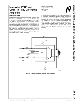
  • 1. Improving PSRR and CMRR in Fully Differential Amplifiers Introduction Power Supply Rejection Ratio (PSRR) and Common Mode Rejection Ratio (CMRR) are the two key specifications when it comes to characterizing and designing differential amplifi- ers. Although these amplifiers are designed to give best PSRR and CMRR performance, a careless application de- sign and a poor selection of external components can sig- nificantly affect these specifications and degrade the overall performance. In this application note, we will look at some of the effects that external components have on PSRR and CMRR: mismatched external gain-setting resistors, the role of the bypass capacitor on PSRR, and some layout tech- niques that improve CMRR and PSRR. In Figure 1, a typical fully differential amplifier block diagram is shown with external gain resistors and an optional bias generator bypass capacitor. DC outputs at Vo1 and Vo2 are biased to half-VDD by internal bias circuitry. AC signals at Vo1 and Vo2 are 180˚ out of phase with respect to each other, creating a Bridge-Tied-Load (BTL) configuration. These amplifiers run with minimal component count, reduc- ing layout time and system cost. Care must be taken to achieve the best possible performance from these amplifiers. 20182501 FIGURE 1. Fully Differential Amplifier Block Diagram National Semiconductor Application Note 1447 Kashif Javaid July 2006 Improving PSRR and CMRR in Fully Differential Amplifiers AN-1447 © 2006 National Semiconductor Corporation AN201825 www.national.com
  • 2. Application Information MEASURING POWER SUPPLY REJECTION RATIO (PSRR) The type of PSRR we are interested in here is an AC specification measuring the ability of the amplifier to reject AC-ripple voltage on the power supply bus, as opposed to a DC specification where we measure the change in output voltage for a change in supply voltage. Basically, ripple PSRR is the ratio of the differential output voltage to the supply ripple voltage expressed in dB as shown in Equation 1. (1) A test circuit for measuring PSRR is shown in Figure 2. The amplifier’s AC inputs are terminated to GND with a low value resistor—typically 10Ω. The value of the input capacitors Ci1 and Ci2 should be matched as closely as possible. Any mismatch can compromise PSRR performance at low fre- quencies. An alternate solution is the elimination of input coupling capacitors terminating the inputs directly to GND. A low-level AC voltage, in the range of 100mVpp to 500mVpp is combined with VDD. This AC plus DC signal is applied to the amplifier’s VDD pin. Any residual AC signal at the ripple frequency present across the BTL outputs is a function of the amplifier’s PSRR. The magnitude of this residual signal is measured with an FFT (using a spectrum analyzer or Audio Precision instrument). Using Equation 1 gives the PSRR value in dB. MEASURING COMMON MODE REJECTION RATIO (CMRR) Common Mode Rejection Ratio is an ability of the differential amplifier to reject common mode input signal and is ex- pressed in dB as shown in Equation 2. (2) A test circuit for measuring CMRR is shown is Figure 3. The amplifier’s AC inputs are connected to a common-mode AC input. Output can be measured by using a high precision AC Volt Meter or Audio Precision instrument. Equation 2 gives the CMRR measurement in dB. For differential input ampli- fiers with external gain-settings resistors, CMRR measure- ment is highly dependent on external resistors as well as board layout. This will be fully discussed in the next section. As a side note, a lot of newer audio measuring instruments such as Audio Precision can perform the CMRR test (and a lot of other audio parameters as well) automatically. 20182533 FIGURE 2. PSRR Measurement Test Circuit AN-1447 www.national.com 2
  • 3. Application Information (Continued) EFFECTS OF EXTERNAL GAIN RESISTORS It is extremely important to match the input resistors to each other as well as the feedback resistors to each other for best CMRR performance. When the inputs of the fully differential amplifier are DC-coupled, resistor matching differences gen- erate net DC currents across the load because of the bal- anced nature of the differential amplifiers. Internally these amplifiers consist of two circuits: a differen- tial amplifier and a common-mode feedback amplifier that adjusts the output voltages so that the nominal DC output bias remains VDD/2. Assuming that the amplifier’ has two equal “halves.” Equation 3 can be obtained by the simple analysis of the differential amplifier in Figure 1 with Vcmi = 0V. Each half uses an input and feedback resistor (Ri and Rf) and contributes to each side of the equation. This equation shows an output offset DC voltage that can result because of resistor mismatching either between feedback resistors (Rf1 and Rf2) or input resistors (Ri1 and Ri2). (3) Ideally, when Ri1 = Ri2 and Rf1 = Rf2, we get perfectly matched and balanced input and feedback resistors pairs and no offset voltage. But if, for example, we assume: Ri1 = Ri2 = R Rf1 = 0.8R and Rf2 = 1.2R, with 20% tolerance in the feedback resistors. We will get an offset voltage of about 0.45 Volts and load current of about 46mA assuming an 8Ω load connected across the output. Now that’s quite a big DC offset voltage! As a result, this reduces the battery life and could affect the speaker performance significantly because of extra DC cur- rent flowing through the voice coil. Common Mode Rejection Ratio is a parameter that can be gravely affected by mis- matched gain resistors. A graph of Common Mode Rejection Ratio vs. feedback resistor mismatch is shown in Figure 4. As can be seen in the graph, a feedback resistor mismatch of 0.4 reduces the CMMR approximately 23dB from the ideal condition perfectly matched resistor. PSRR is also affected by the gain resistors mismatch, but with a small capacitor on the bypass pin this effect is re- duced extensively and yields practically no effect at all on the power supply rejection. The effects of bypass capacitor will be fully discussed in the next section. Thus, for all practical purpose, resistors of 1% tolerance or even better should be used for optimal performance and best common mode re- jection ratio. 20182507 FIGURE 3. CMRR Measurement Test Circuit AN-1447 www.national.com 3
  • 4. Application Information (Continued) EFFECTS OF BYPASS CAPACITOR Fully differential amplifiers offer an “optional” bypass capaci- tor (CB) and allow a designer to use these amplifiers with minimal component count. Before eliminating the optional bypass capacitor to reduce component count, one should understand how that might affect the overall performance of the amplifier. Internally, a common mode amplifier adjusts the two outputs to a quiescent DC voltage equal to halve- VDD. Any supply fluctuations cause both outputs to move in phase. This ideally creates a net change of 0VDC differen- tially across the outputs. Thus, a bypass capacitor is not really required and can be considered optional. But in the real world, these amplifiers are not perfect. Furthermore, mismatch in the external resistors can result in unbalanced amplifier operation. PSRR is the most important parameter that would be affected significantly by eliminating the bypass capacitor. Differential input amplifiers are considered excellent low noise and high PSRR amplifiers when compared to similar single-ended amplifiers. As shown in Figure 5 at low ripple frequencies, the PSRR is close to 70dB, even without a bypass capacitor. However, using a bypass capacitor in range of 0.1 uF to 1 uF offers a significant 20dB PSRR improvement. Depending upon the application, PSRR of 70dB might be considered good and more than adequate for most applications. However, in cell-phone market where an excellent PSRR is desired, particularly at lower frequencies, 20182535 FIGURE 4. CMRR vs Feedback Resistor Mismatch 20182536 FIGURE 5. PSRR vs Ripple Frequency AN-1447 www.national.com 4
  • 5. Application Information (Continued) adding a bypass capacitor certainly will improve the lower frequencies power supply rejection. Furthermore, the ampli- fier will be less sensitive to slight gain resistor value mis- match. LAYOUT CONSIDERATIONS Printed circuit board layout is generally considered to be very application specific. Nevertheless, it is possible to ob- serve some guidelines that optimize the overall performance of the amplifier. Fully differential amplifiers come in different packages. Please contact the National Semiconductor Corp. website for package-specific applications information before attempt- ing to start any new layout. Another important factor to consider is star ground vs. ground plane. This is very appli- cation and package specific. Either configuration is used when combined with the following general suggestions: a) Make use of symmetrical placement of components (i.e. feedback resistors and input resistors). b) If not using ground planes, VDD and GND traces should be as wide as possible. c) If a heat-sink plane is desired for exposed-DAP pack- ages, it should be appropriately sized. Refer to the power derating graphs in the corresponding datasheet. d) The distance between the chip and any possible antenna source should be as far as possible. e) If possible, make the output traces short and equal in length and away from the any antenna source. f) If using a star ground, all the GNDs such as bypass capacitor GND, supply capacitor GNDs, and any other sys- tem ground should be directly connected to a single point on the board, possibly at the board’s point of entry for the power supply GND. AN-1447 www.national.com 5
  • 6. Revision Table Rev Date Description 1.0 04/20/06 Initial release. 1.1 07/24/06 Simple text edits, then re-released the App Notes into the WEB. National does not assume any responsibility for use of any circuitry described, no circuit patent licenses are implied and National reserves the right at any time without notice to change said circuitry and specifications. For the most current product information visit us at www.national.com. LIFE SUPPORT POLICY NATIONAL’S PRODUCTS ARE NOT AUTHORIZED FOR USE AS CRITICAL COMPONENTS IN LIFE SUPPORT DEVICES OR SYSTEMS WITHOUT THE EXPRESS WRITTEN APPROVAL OF THE PRESIDENT AND GENERAL COUNSEL OF NATIONAL SEMICONDUCTOR CORPORATION. As used herein: 1. Life support devices or systems are devices or systems which, (a) are intended for surgical implant into the body, or (b) support or sustain life, and whose failure to perform when properly used in accordance with instructions for use provided in the labeling, can be reasonably expected to result in a significant injury to the user. 2. A critical component is any component of a life support device or system whose failure to perform can be reasonably expected to cause the failure of the life support device or system, or to affect its safety or effectiveness. BANNED SUBSTANCE COMPLIANCE National Semiconductor follows the provisions of the Product Stewardship Guide for Customers (CSP-9-111C2) and Banned Substances and Materials of Interest Specification (CSP-9-111S2) for regulatory environmental compliance. Details may be found at: www.national.com/quality/green. Lead free products are RoHS compliant. National Semiconductor Americas Customer Support Center Email: new.feedback@nsc.com Tel: 1-800-272-9959 National Semiconductor Europe Customer Support Center Fax: +49 (0) 180-530 85 86 Email: europe.support@nsc.com Deutsch Tel: +49 (0) 69 9508 6208 English Tel: +44 (0) 870 24 0 2171 Français Tel: +33 (0) 1 41 91 8790 National Semiconductor Asia Pacific Customer Support Center Email: ap.support@nsc.com National Semiconductor Japan Customer Support Center Fax: 81-3-5639-7507 Email: jpn.feedback@nsc.com Tel: 81-3-5639-7560 www.national.com AN-1447 Improving PSRR and CMRR in Fully Differential Amplifiers