This document describes the design of different types of parallel multipliers using low power techniques on a 0.18um technology node. It discusses Braun multipliers, row bypassing multipliers, and column bypassing multipliers. The multipliers are implemented using both conventional CMOS design and the Gate Diffusion Input (GDI) technique. Simulation results show that implementing the multipliers using GDI reduces transistor count and power consumption compared to the conventional design. The column bypassing multiplier implemented with GDI has the lowest power consumption of 3.4mw. In conclusion, combining row and column bypassing in a 2D multiplier design results in lower delay and power than the individual approaches.


![ISSN: 2278 – 1323
International Journal of Advanced Research in Computer Engineering & Technology (IJARCET)
Volume 2, Issue 7, July 2013
2362
www.ijarcet.org
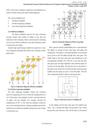
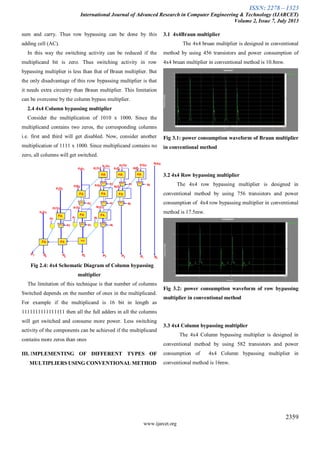
Fig 5.3: power consumption waveform of column bypass
multiplier in GDI method
VI. COMPARISON RESULTS BETWEEN
CONVENTIONAL METHOD AND GDI TECHNIQUE
6.1 area comparision between conventional method and
GDI technique
Fig 5.3: area comparision between conventional method
and GDI technique
6.2 comparision of power consumption between
conventional method and GDI technique
Fig 5.3: area comparision between conventional method
and GDI technique
VII. CONCLUSION
Thus the hardware implementation of Braun, Row, column
multiplier and 2-D multiplier gave the difference in time
delays for each computation is compared in the previous slide
through graphical representation.
By combining both row bypassing and column bypassing
multipliers we have produced a 2-D bypassing multiplier with
less delay and power consumption.
Based on the simplification of the MAC operations and by
using low-power bypassing technique, we have designed a
two dimensional multiplier which has less computations and
less switching activities with low power consumption.
REFERENCES
[1] Oscal T. -C. Chen, Sandy Wang, and Yi-Wen
Wu, .Minimization of Switching Activities of Partial Products
for Designing Low-Power Multipliers., IEEE Transactions on
VLSI Systems, June 2003 vol. 11, no.3.
[2] HichemBelhadj, BehroozZahiri, Albert Tai .Power-
sensitive design techniques on FPGA devices. Proceedings of
International conference on IC Taipai (2003).
[3] S. Hong, S. Kim, M.C. Papaefthymiou, and W.E.
Stark, .Low power parallel multiplier design for DSP
applications through coefficient optimization. In Proc. of
Twelfth Annual IEEE Int. ASIC/SOC onf., Sep. 1999, pp.
286-290.
[4]I. S. Abu-Khater, A. Bellaouar, and M. Elmasry, .Circuit
techniques for CMOS low-power high-performance
multipliers., IEEE J. Solid-State Circuits, Oct. 1996, vol. 31,
pp. 1535.1546.](https://image.slidesharecdn.com/ijarcet-vol-2-issue-7-2357-2362-130827222900-phpapp01/85/Ijarcet-vol-2-issue-7-2357-2362-6-320.jpg)