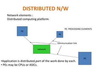
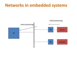
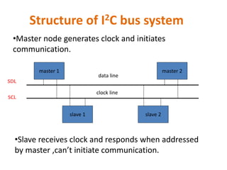
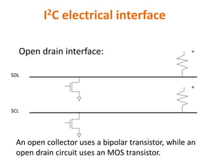
MICROPROCESSOR APPLICATION IN
INDUSTRIAL CONTROL
I2C bus
By-Er. Payal Suthar
ME STUDENT
DISTRIBUTED N/W
PE
PE
PE
network
communication link
Network elements :
Distributed computing platform:
•Application is distributed,part of the work done by each.
• PEs may be CPUs or ASICs.
PE: PROCESSING ELEMENTS
Networks in embedded systems
PE
PE sensor
PE actuator
initial processing
more processing
Why distributed N/W Necessary?
• Because the devices that the PEs
communicate with are physically separated.
• Improved debugging , use one CPU in network
to debug others.
•One part of the system can be used to help
diagnose problems in another part.
I2C BUS
• Commonly used to link microcontroller into
system
• Low cost, easy to implement
• Has moderate speed
• (100kbps for std bus ,400kbps for extended
bus)
Structure of I2C bus system
master 1 master 2
slave 1 slave 2
SCL
SDL
data line
clock line
•Master node generates clock and initiates
communication.
•Slave receives clock and responds when addressed
by master ,can’t initiate communication.
I2C electrical interface
SDL
+Open drain interface:
SCL
+
An open collector uses a bipolar transistor, while an
open drain circuit uses an MOS transistor.
Open drain interface
Voltage used are +5V or +3.3V
I2C Physical Protocol
Two special sequence 1)start,2)stop
Cont…
•Data is transferred in sequence of 8 bit.
•Starting with MSB.
•9th bit is ack bit so 9 scl clock to transfer 8
bit.
I2C Device Addressing
•R/W=0 :master writing, R/W=1 : master reading
•R/W bit makes it an odd/ even address.
•Ack =0 :it has received data and ready to accept
another data.
•Ack=1 : it can’t accept further data, master should
terminate transfer with stop sequence.
Typical bus transactions on the I2C bus
Timing diagram
•Data Transfer is initiated with a START bit (S) signaled by SDA being pulled low
while SCL stays high.
•SDA sets the 1st data bit level while keeping SCL low (during blue bar time.)
•The data is sampled (received) when SCL rises (green) for the first bit (B1).
•This process repeats, SDA transitioning while SCL is low, and the data being
read while SCL is high (B2, Bn).
•A STOP bit (P) is signaled when SDA is pulled high while SCL is high.
•In order to avoid false marker detection, SDA is changed on the SCL falling edge
and is sampled and captured on the rising edge of SCL.
An I2C interface in a
microcontroller.

I2C BUS

  • 1.
    MICROPROCESSOR APPLICATION IN INDUSTRIALCONTROL I2C bus By-Er. Payal Suthar ME STUDENT
  • 2.
    DISTRIBUTED N/W PE PE PE network communication link Networkelements : Distributed computing platform: •Application is distributed,part of the work done by each. • PEs may be CPUs or ASICs. PE: PROCESSING ELEMENTS
  • 3.
    Networks in embeddedsystems PE PE sensor PE actuator initial processing more processing
  • 4.
    Why distributed N/WNecessary? • Because the devices that the PEs communicate with are physically separated. • Improved debugging , use one CPU in network to debug others. •One part of the system can be used to help diagnose problems in another part.
  • 5.
    I2C BUS • Commonlyused to link microcontroller into system • Low cost, easy to implement • Has moderate speed • (100kbps for std bus ,400kbps for extended bus)
  • 6.
    Structure of I2Cbus system master 1 master 2 slave 1 slave 2 SCL SDL data line clock line •Master node generates clock and initiates communication. •Slave receives clock and responds when addressed by master ,can’t initiate communication.
  • 7.
    I2C electrical interface SDL +Opendrain interface: SCL + An open collector uses a bipolar transistor, while an open drain circuit uses an MOS transistor.
  • 8.
    Open drain interface Voltageused are +5V or +3.3V
  • 9.
    I2C Physical Protocol Twospecial sequence 1)start,2)stop
  • 10.
    Cont… •Data is transferredin sequence of 8 bit. •Starting with MSB. •9th bit is ack bit so 9 scl clock to transfer 8 bit.
  • 11.
    I2C Device Addressing •R/W=0:master writing, R/W=1 : master reading •R/W bit makes it an odd/ even address. •Ack =0 :it has received data and ready to accept another data. •Ack=1 : it can’t accept further data, master should terminate transfer with stop sequence.
  • 12.
  • 13.
    Timing diagram •Data Transferis initiated with a START bit (S) signaled by SDA being pulled low while SCL stays high. •SDA sets the 1st data bit level while keeping SCL low (during blue bar time.) •The data is sampled (received) when SCL rises (green) for the first bit (B1). •This process repeats, SDA transitioning while SCL is low, and the data being read while SCL is high (B2, Bn). •A STOP bit (P) is signaled when SDA is pulled high while SCL is high. •In order to avoid false marker detection, SDA is changed on the SCL falling edge and is sampled and captured on the rising edge of SCL.
  • 14.
    An I2C interfacein a microcontroller.