1) The document presents a simulation of a graphene field-effect transistor (GFET) using technology computer-aided design (TCAD) software to analyze the influence of different top-gate dielectric materials.
2) The simulation shows that using high-k dielectric materials like hafnium oxide and aluminum oxide improves the electrical properties of the GFET, increasing saturation drain current and the on/off current ratio compared to silicon-based dielectric materials.
3) Varying the thickness of the dielectric materials, the simulation found that a very thin layer of high-k dielectric is needed to maximize the critical electrical parameters of the GFET.
This document summarizes a seminar presentation on high-k dielectric devices. It begins by explaining the problems with further scaling silicon dioxide gate dielectrics due to tunneling currents. It then introduces high-k dielectric materials, which have a higher dielectric constant, allowing for thicker dielectric layers with equivalent capacitance. The document discusses issues with compatibility between polysilicon gates and high-k dielectrics, leading to the use of metal gates. It presents the high-k dielectric - metal gate solution adopted by Intel and others, which reduces gate leakage currents and increases performance. Finally, it discusses future opportunities in using high-k dielectrics with non-silicon substrates like germanium.
Carbon nanotube field-effect transistors (CNTFETs) have advantages over traditional MOSFETs by avoiding issues like short channel effects and high leakage currents that arise from continuous MOSFET scaling. CNTFETs use carbon nanotubes that can be metallic or semiconducting depending on their structure. They have a similar structure to MOSFETs but current flow depends on ballistic transport and electron confinement in the CNT. CNTFETs also have lower quantum capacitance than MOSFETs, resulting in lower propagation delay. Neural networks are well-suited for modeling CNTFETs with their simple, continuous equations that can account for channel length variations. However, precisely controlling CNT
Microelectronic technology
This report briefly discusses the need for Metal-Oxide-Semiconductor Field Effect Transistors (MOSFETs), their structure and principle of operation. Then it details the fabrication and characterization of the MOSFETs fabricated at the microelectronic lab at University of Malaya
shows the simulation and analysis of a MOSFET device using theĀ MOSFetĀ tool. Several powerful analytic features of this tool are demonstrated, including the following:
ļcalculation of Id-Vg curves
ļpotential contour plots along the device at equilibrium and at the final applied bias
ļelectron density contour plots along the device at equilibrium and at the final applied bias
ļspatial doping profile along the device
ļ1D spatial potential profile along the device
This document discusses carbon nanotube field-effect transistors (CNTFETs) as a potential substitute for MOSFETs. CNTFETs could help overcome limitations of MOSFET scaling by providing higher carrier mobility, excellent electrostatics, and gate control. CNTFETs exhibit advantages like better threshold voltage and subthreshold slope control as well as higher current density and transconductance compared to MOSFETs. However, mass production of CNTFETs faces challenges related to defects, failure rates, and production costs that are higher than for traditional CMOS.
The document discusses carbon nanotube field effect transistors (CNTFETs) as a potential replacement for MOSFETs. It describes some of the issues with continuously scaling down MOSFETs, and then provides details on different types of CNTFET designs and their advantages over MOSFETs, such as higher carrier mobility and transconductance. Some applications of CNTFETs are also mentioned. However, drawbacks include higher production costs and failure rates compared to traditional CMOS technology.
High electron mobility transistor(hemt)MonikaSaleth
Ā
The document summarizes the High Electron Mobility Transistor (HEMT), a type of field effect transistor used for applications requiring low noise and high performance at microwave frequencies. HEMTs utilize a hetero-junction consisting of different materials on either side of a PN junction. Common materials are Aluminum Gallium Arsenide and Gallium Arsenide. HEMTs offer advantages like high gain, switching speed, and efficiency for applications from 5-100 GHz, including telecommunications, radar, and other RF designs.
This document discusses junctionless transistors as an alternative to traditional transistors. Junctionless transistors have no p-n junctions and instead use uniformly doped semiconductor material. They offer advantages like simpler fabrication without implantation or annealing steps, reduced short channel effects, higher carrier mobility, and lower leakage current. However, they can have greater threshold voltage variability than conventional transistors. The document provides details on the structure and operation of junctionless transistors, comparing them to traditional transistors and discussing their potential to enable further device miniaturization.
This document summarizes the double-gate MOSFET transistor. It begins by describing the basic operation of a single-gate MOSFET and then discusses the scaling limitations of bulk MOSFETs, such as decreasing carrier mobility and threshold voltage rolloff as channel length decreases. It introduces the double-gate MOSFET as a way to better control the channel and reduce short-channel effects. Key features of the double-gate MOSFET include two gates that control the ultra-thin body channel and allow direct scaling to small channel lengths of 20nm or less. Fabricating double-gate MOSFETs using a silicon-on-insulator approach provides benefits like low leakage currents. The double gates provide improved performance
HEMTs (High Electron Mobility Transistors) are transistors that use a heterojunction between two semiconductor materials with different band gap energies to confine electrons in a 2D gas layer. This results in much higher electron mobility than conventional transistors, allowing HEMTs to operate at higher speeds with lower noise. Key features include a heterojunction interface that forms a potential well trapping electrons, reducing scattering and increasing mobility. Initial applications were in high-speed microwave devices, and HEMTs are now widely used in cell phones and other wireless technologies.
This document discusses resonant tunneling diodes (RTDs). It begins by motivating the need for signal sources at very high frequencies beyond what conventional transistors can provide. It then introduces normal tunneling diodes and their limitations. RTDs are described as using quantum wells and barriers to allow tunneling only when electrons have a certain minimum energy. This produces negative differential resistance which can be used for oscillation. While RTDs are very fast devices, their output current and power is limited compared to other technologies. More research is needed to improve their power and integration.
This document provides an overview of FinFET technology. It defines FinFET as a non-planar, double gate transistor built on an SOI substrate, where the conducting channel is wrapped by a thin silicon fin. Due to its dual gate structure, FinFET has better control over short channel effects compared to planar MOSFETs. It also allows for higher integration density than planar MOSFETs. Additionally, FinFET fabrication is relatively simple. The document discusses FinFET structure, recent developments, fabrication mechanisms, advantages/limitations, and applications.
This presentation summarizes research on junctionless transistors and their applications. It introduces junctionless transistors as an alternative to traditional junction transistors that can help address challenges from Moore's Law like power consumption and short channel effects. The presentation describes the structure and operation of junctionless transistors. It then compares junctionless transistors to junction transistors, highlighting advantages like lower electric fields, easier fabrication, and reduced short channel effects. Several applications are discussed, with a focus on using junctionless transistors in DRAM to improve retention time and sense margin. Results are presented on optimizing the performance of double-gate junctionless transistors by varying length, thickness, and doping concentration. The conclusion discusses the near ideal subthreshold slope and potential for digital applications. Future
This document discusses simulations of carbon nanotube, graphene, and silicon nanowire field effect transistors. It outlines objectives to review nanodevices, simulate different nanodevice structures to study characteristics, and compare results. Sections describe the structures, parameters varied in simulation like dielectric constant and channel length, and results showing the impact on performance metrics like on/off ratio. Future work and conclusions note limitations and potential for further simulation to better optimize device design.
1. Fully Depleted Silicon On Insulator (FD-SOI) is an innovation that uses an ultra-thin silicon film and buried oxide layer to improve transistor performance and reduce leakage currents.
2. By using a thin buried oxide and silicon film, FD-SOI allows the depletion region to cover the entire film, improving electrostatic characteristics and reducing parasitic capacitance compared to bulk transistors.
3. The improvements allow FD-SOI transistors to operate faster at lower voltages while significantly reducing leakage currents and improving power efficiency through improved body biasing controls.
Quantum dots are tiny semiconductor crystals between 2-10 nanometers in size. Their properties depend on factors like size and energy levels. Smaller quantum dots emit higher frequency/shorter wavelength blue light while larger dots emit lower frequency/longer wavelength red light. Quantum dots have potential applications in solar cells, displays, and medical imaging due to their tunable light emission and other optical properties. They are typically made through colloidal synthesis which allows for mass production under mild conditions.
The document discusses carbon nanotube field-effect transistors (CNTFETs) as an alternative to MOSFETs. It notes that continued scaling of MOSFETs faces challenges like short channel effects and high leakage currents. CNTFETs offer potential advantages like ballistic transport and high mobility. The document describes the basic structure and working of different types of CNTFETs, including bottom-gate, top-gate, coaxial gate, Schottky-barrier, and MOSFET-like devices. It compares key metrics of CNTFETs like transconductance and drive current to MOSFETs. In conclusion, CNTFETs show promise for high performance if manufacturing challenges can be addressed.
This document discusses using graphene for electronic devices. It describes how graphene's zero bandgap is problematic for digital electronics but its high mobility makes it promising. Several approaches are presented to induce a bandgap, including using graphene nanoribbons, applying a vertical electric field to bilayer graphene, and creating lateral heterostructures with materials of different bandgaps. Modeling shows these approaches can effectively control the band structure and enable transistor operation. Challenges remain in fabricating devices with sufficient reproducibility and without degrading carrier mobility. Lateral heterostructure FETs are identified as one of the most promising device concepts.
The document discusses the history and development of FinFET transistors. FinFETs were developed to overcome short channel effects by using a thin silicon fin as the channel between the source and drain. This allows the gate to control the channel from both sides and edges of the fin. FinFET fabrication involves depositing fins using electron beam lithography then depositing a gate material around the fins. FinFETs suppress short channel effects and allow for higher density transistors compared to planar MOSFETs, though they also have some disadvantages like reduced mobility.
Introduction to FINFET, Details of FinFETJustin George
Ā
1) The document discusses FinFET, a type of non-planar transistor used in modern semiconductor fabrication. It describes the construction of FinFET which involves etching fins on an SOI substrate and wrapping gates around the fins.
2) FinFET works by having an elevated fin-shaped channel that the gate wraps around. This allows FinFET to operate at lower voltage and offer higher drive current compared to planar transistors.
3) FinFET technology is being widely adopted in integrated circuits due to advantages like suppressed short channel effect, better drive current, lower leakage power, and no random dopant fluctuation.
Intel has achieved a breakthrough in transistor technology by developing high-k + metal gate transistors for its 45 nm process. These transistors significantly reduce leakage power and are the biggest advancement since polysilicon gate MOS transistors were introduced in the 1960s. Intel has made working 45 nm microprocessors using these new transistors, which will deliver higher performance and greater energy efficiency. Intel's 45 nm products are on track to begin production in late 2007 with three factories manufacturing 45 nm by early 2008.
Short Channel Effects are governed by complex physical phenomena and mainly Influenced because of both vertical and horizontal electric field components.
To meet the current requirements of
Electronic devices, the miniaturization of devices is important. And so is Second Order effects which otherwise degrade the performance of devices.
The document discusses various techniques for electrically isolating devices in integrated circuits. It describes junction isolation, which uses reverse biased PN junctions, but this did not scale well as devices became smaller. Dielectric isolation techniques like LOCOS and STI were developed using deposited or thermally grown oxides. LOCOS had limitations like bird's beak encroachment affecting small device areas. STI involves etching trenches and depositing oxide to fill them, avoiding issues with LOCOS at small scales.
Semiconductors are materials that have electrical conductivity between conductors such as most metals and nonconductors or insulators like ceramics. How much electricity a semiconductor can conduct depends on the material and its mixture content.
Semiconductors can be insulators at low temperatures and conductors at high temperatures. As they are used in the fabrication of electronic devices, semiconductors play an important role in our lives.
The document discusses the insulated gate bipolar transistor (IGBT), a three-terminal power semiconductor device primarily used as an electronic switch. IGBTs combine high efficiency and fast switching. They have lower conduction losses than other devices, can block larger voltages, and have small turn-on and turn-off times. The document describes the basic IGBT structure, punch-through and non-punch-through variations, and their off-state and on-state operations. It notes applications of IGBTs include medium-power devices like motor drives, solid-state relays, and high-frequency signal choppers.
The document discusses tunnel field-effect transistors (TFETs) as a potential next-generation transistor technology. It presents a simulation comparing an InAs homojunction TFET to an NMOS transistor. The simulation shows the TFET has superior subthreshold swing and on/off ratio compared to the NMOS, though the NMOS has higher power. The TFET operates via band-to-band tunneling rather than thermal injection like in traditional transistors.
1. The document discusses the static characteristics of MOS inverters, including their voltage transfer characteristic (VTC). The VTC describes the output voltage (Vout) as a function of the input voltage (Vin) under DC conditions.
2. Key parameters that determine the VTC include the threshold voltage of the driver transistor (VT0), the product of kn and the load resistance (knRL), and the power supply voltage (VDD). Larger knRL results in a steeper transition slope and smaller output low voltage (VOL).
3. Calculations are shown for determining the output high (VOH) and low (VOL) voltages, as well as the input voltages (VIL,
This document outlines a study conducted by Harshit Soni under the supervision of Dr. MM Tripathi at Delhi Technological University. It compares the performance of conventional trench gate MOSFETs, buffered trench gate MOSFETs, and GaN-buffered trench gate MOSFETs through TCAD simulation. The key findings are that GaN-BTG MOSFETs exhibit superior electric field, electron velocity, drain current, and transconductance compared to other designs. GaN-BTG MOSFETs also have lower threshold voltage and off-current, indicating better performance for low power applications.
Modeling of Dirac voltage for highly p-doped graphene field-effect transistor...journalBEEI
Ā
In this paper, the modeling approach of Dirac voltage extraction of highly p-doped graphene field-effect transistor (GFET) measured at atmospheric pressure is presented. The difference of measurement results between atmospheric and vacuum pressures was analyzed. This work was started with actual wafer-scale fabrication of GFET with the purposes of getting functional device and good contact of metal/graphene interface. The output and transfer characteristic curves were measured accordingly to support on GFET functionality and suitability of presented wafer fabrication flow. The Dirac voltage was derived based on the measured output characteristic curve using ambipolar virtual source model parameter extraction methodology. The circuit-level simulation using frequency doubler circuit shows the importance of accurate Dirac voltage value to the device practicality towards design integration.
Modeling of dirac voltage for highly p doped graphene field effect transistor...Journal Papers
Ā
This document presents a methodology for modeling the Dirac voltage of a highly p-doped graphene field-effect transistor (GFET) measured at atmospheric pressure. A GFET was fabricated through a wafer-scale process and its output and transfer characteristics were measured. Due to interactions with water molecules in the air, the Dirac voltage was shifted to a very high positive value and could not be determined from the transfer curve alone. To address this, a correlation factor was derived by comparing commercial GFET measurements in air and vacuum. This factor was used to project the fabricated GFET's output curve to vacuum conditions. An ambipolar virtual source model was then fitted to the projected curve to extract model parameters and simulate the transfer curve, revealing the
Modeling of dirac voltage for highly p doped graphene field effect-transistor...Conference Papers
Ā
The document presents a modeling approach to extract the Dirac voltage from transfer characteristics of a highly p-doped graphene field-effect transistor (GFET) measured at atmospheric pressure. It describes the full wafer-scale fabrication process used to produce the GFET devices and issues with characterizing them at atmospheric pressure due to water molecule absorption. The modeling approach projects the output characteristics to vacuum pressure conditions using a correlation factor from a commercial GFET sample, then fits an ambipolar virtual source model to the data to determine the Dirac voltage.
Optimization of 14 nm double gate Bi-GFET for lower leakage currentTELKOMNIKA JOURNAL
Ā
In recent years, breakthroughs in electronics technology have resulted in upgrades in the physical properties of the metal oxide semiconductor field effect transistor (MOSFET) toward smaller sizes and improvements in both quality and performance. Hence, the growth field effect transistor (GFET) is being promoted as one of the worthy contenders due to its superior material characteristics. A 14 nm horizontal double-gate bilayer graphene FET with a high-k/metal gate is proposed, which is composed of hafnium dioxide (HfO2) and tungsten silicide (WSix) respectively. It is simulated and modelled using silvaco ATHENA and ATLAS technology computer-aided design (TCAD) tools, as well as the Taguchi L9 orthogonal array (OA). The threshold voltage (VTH) adjustment implant dose, VTH adjustment implant energy, source/drain (S/D) implant dose, and S/D implant energy have all been investigated as process parameters. While the VTH adjustment tilt angle and the S/D implant tilt angle have both been investigated as noise factors. When compared to the initial findings before optimization, the IOFF has a value of 29.579 nA/Āµm, indicating a significant improvement. Findings from the optimization technique demonstrate excellent device performance with an IOFF of 28.564 nA/Āµm, which is closer to the international technology roadmap semiconductor (ITRS) 2013 target than before
The document describes a simulation study comparing the RF and analog performance of different AlGaN/GaN MOSHEMT device structures. Single gate MOSHEMTs using SiO2, Al2O3, and HfO2 dielectrics were designed and simulated. Double gate and dielectric pocket double gate MOSHEMT structures were also simulated to improve performance. Simulation results showed the HfO2 dielectric pocket double gate MOSHEMT achieved the best performance with high drain current and transconductance, as well as high cutoff frequency over 1.95 THz, indicating suitability for analog and millimeter-wave applications.
Modeling and Simulation Graphene based Nano FET : A ReviewIRJET Journal
Ā
The document discusses modeling and simulation of graphene-based nano field effect transistors (FETs). It describes using the SILVACO TCAD tools to build a device structure in ATLAS and model a graphene FET with graphene as the channel material. The output characteristic and transfer curve are plotted. While graphene FETs have extremely high carrier mobility, they lack a bandgap and have a lower on-off current ratio than silicon transistors. However, they are well-suited for radio frequency applications due to their high mobility. The document also reviews related works on graphene FET modeling and applications.
We present this work by two steps. In the first one, the new structure proposed of the FP-HEMTs device (Field plate High Electron Mobility Transistor) with a T-gate on an 4H-SIC substrate to optimize these electrical performances, multiple field-plates were used with aluminum oxide to split the single electric field peak into several smaller peaks, and as passivation works to reduce scaling leakage current. In the next, we include a modeling of a simulation in the Tcad-Silvaco Software for realizing the study of the influence of negative voltage applied to gate T-shaped in OFF state time and high power with ambient temperature, the performance differences between the 3FP and the SFP devices are discussed in detail.
OFET Preparation by Lithography and Thin Film Depositions ProcessTELKOMNIKA JOURNAL
Ā
This document summarizes research on preparing an organic field-effect transistor (OFET) using lithography and thin film deposition processes. The key points are:
1. An OFET was prepared with a bottom contact structure using copper phthalocyanine as the active layer deposited via vacuum evaporation on a silicon substrate.
2. Lithography was used to pattern gold source and drain electrodes, followed by deposition of the copper phthalocyanine thin film.
3. Electrical characterization of the completed OFET showed current increasing with drain voltage and gate voltage, indicating p-type accumulation mode operation, though saturation was not observed possibly due to a high threshold voltage.
Simulations of the CNFETs using different high-k gate dielectricsjournalBEEI
Ā
In this paper we presented the analysis of Carbon Nanotube Field Effect Transistors (CNFETs) using various high-k gate dielectric materials. The objective of this work was to choose the best possible material for gate dielectric. This paper also presented the study on the effect of thickness of gate dielectric on the performance of the device. For the analysis (19, 0) CNT was considered because the diameter of (19, 0) CNT is 1.49nm and the CNFETs have been fabricated with the CNT diameter of ~1.5nm. It has been observed that La2O3 is the best gate dielectric material followed by HfO2 and ZrO2. It was also observed that as thickness of gate dielectric material reduces, drain current of CNFET increases. The outcomes of this study matches with the analytical results and hence confirm the results.
Performance Evaluation of GaN Based Thin Film Transistor using TCAD Simulation Yayah Zakaria
Ā
As reported in past decades, gallium nitride as one of the most capable compound semiconductor, GaN-based high-electron mobility transistors are the focus of intense research activities in the area of high power, high-speed, and high-temperature transistors. In this paper we present a design and simulation of the GaN based thin film transistor using sentaurus TCAD for
the extracting the electrical performance. The resulting GaN TFTs exhibits good electrical performance in the simulated results, including, a threshold voltage of 12-15 V, an on/off current ratio of 6.5Ć10 7 ~ 8.3Ć10 and a subthreshold slope
of 0.44V/dec. Sentaurus TCAD simulations is the tool which
offers study of comprehensive behavior of semiconductor structures with ease. The simulation results of the TFT structure based on gallium nitride active channel have great prospective in the next-generation flat-panel display applications.
Performance Evaluation of GaN Based Thin Film Transistor using TCAD Simulation IJECEIAES
Ā
As reported in past decades, gallium nitride as one of the most capable compound semiconductor, GaN-based high-electron mobility transistors are the focus of intense research activities in the area of high power, high-speed, and high-temperature transistors. In this paper we present a design and simulation of the GaN based thin film transistor using sentaurus TCAD for the extracting the electrical performance. The resulting GaN TFTs exhibits good electrical performance in the simulated results, including, a threshold voltage of 12-15 V, an on/off current ratio of 6.5Ć10 7 ~ 8.3Ć10 , and a subthreshold slope of 0.44V/dec. Sentaurus TCAD simulations is the tool which offers study of comprehensive behavior of semiconductor structures with ease. The simulation results of the TFT structure based on gallium nitride active channel have great prospective in the next-generation flat-panel display applications.
Electrical bistabilities behaviour of all solution-processed non-volatile mem...Journal Papers
Ā
This document describes an all-solution-processed non-volatile memory device based on graphene quantum dots (GQDs) embedded in graphene oxide layers. The memory device was fabricated on a flexible PET substrate using spin-coating and spray-coating deposition of the layers. Electrical characterization showed bistable switching behavior with an ON/OFF current ratio of 105. Various conduction mechanisms were proposed to describe the charge trapping and transport processes in the GQD-based memory, including Schottky emission, Poole-Frenkel emission, and trapped charge limited current conduction. The GQDs provided nanoscale charge trapping sites to enable multilevel switching and non-volatility in the graphene oxide-based resistive memory structure
Performance analysis of high-k materials as stern layer in ion-sensitive fiel...TELKOMNIKA JOURNAL
Ā
High-k materials as a STERN Layer for Ion-Sensitive-Field-Effect-Transistor (ISFET) have improved ISFET sensitivity and stability. These materials decrease leakage current and increase capacitance of the ISFET gate toward highest current sensitivity. So far, many high-k materials have been utilized for ISFET, yet they were examined individually, or using numerical solutions rather than using integrated TCAD environment. Exploiting TCAD environment leads to extract ISFET equivalent circuit parameters and performs full analysis for both device and circuit. In this study we introduce a comprehensive investigation of different high-k material, Tio2, Ta2O5, ZrO2, Al2O3, HfO2 and Si3N4 as well as normal silicon dioxide and their effects on ISFET sensitivity and stability. This was implemented by developing commercial Silvaco TCAD rather than expensive real fabrication. The results confirm that employing high-k materials in ISFET outperform normal silicon dioxide in terms of sensitivity and stability. Further analysis revealed that Titanium dioxide showed the highest sensitivity followed by two groups HfO2, Ta2O5 and ZrO2, Al2O3 respectively. Another notable exception of Si3N4 that is less than other materials, but still have higher sensitivity than normal silicon dioxide. We believe that this study opens new directions for further analysis and optimization prior to the real cost-ineffective fabrication.
Investigation and design of ion-implanted MOSFET based on (18 nm) channel lengthTELKOMNIKA JOURNAL
Ā
The aim of this study is to invistgate the characteristics of Si-MOSFET with 18 nm length of ion implemented channel. Technology computer aided design (TCAD) tool from Silvaco was used to simulate the MOSFETās designed structure in this research. The results indicate that the MOSFET with 18 nm channel length has cut-off frequency of 548 GHz and transconductance of 967 Ī¼S, which are the most important factors in calculating the efficiency and improving the performance of the device. Also, it has threshold voltage of (-0.17 V) in addition obtaining a relatively small DIBL (55.11 mV/V). The subthreshold slope was in high value of 307.5 mV/dec. and this is one of the undesirable factors for the device results by short channel effect, but it does not reduce its performance and efficiency in general.
EXPERIMENT INVESTIGATION OF EDM PARAMETER MRR AND TWR WITH MULTI WALL CARBON ...IAEME Publication
Ā
This document summarizes an experiment investigating EDM parameters of material removal rate (MRR) and tool wear rate (TWR) using multi-wall carbon nanotubes. Experiments were conducted using an EDM machine to machine EN-31 steel with an aluminum tool electrode. Multi-wall carbon nanotubes were mixed with dielectric fluid at 0.5 g/L. A full factorial design was used to vary peak current, pulse on time, and pulse off time. MRR and TWR were measured and regression models were developed to predict the output parameters. The results showed that on average, MRR improved by 19% while TWR decreased by 8.51% with the addition of multi-wall carbon nanotubes
Design and performance analysis of front and back Pi 6 nm gate with high K d...IJECEIAES
Ā
Advanced high electron mobility transistor (HEMT) with dual front gate, back gate with silicon nitride/aluminum oxide (Si3N4/Al2O3) as passivation layer, has been designed. The dependency on DC characteristics and radio frequency characteristics due to GaN cap layers, multi gate (FG and BG), and high K dielectric material is established. Further compared single gate (SG) passivated HEMT, double gate (DG) passivated HEMT, double gate triple (DGT) tooth passivated HEMT, high K dielectric front Pi gate (FG) and back Pi gate (BG) HEMT. It is observed that there is an increased drain current (Ion) of 5.92 (A/mm), low leakage current (Ioff) 5.54E-13 (A) of transconductance (Gm) of 3.71 (S/mm), drain conductance (Gd) of 1.769 (S/mm), Cutoff frequency (fT) of 743 GHz maximum oscillation frequency (Fmax) 765 GHz, minimum threshold voltage (šš”ā) of -4.5 V, on resistance (Ron) of 0.40 (Ohms) at ššš = 0 V. These outstanding characteristics and transistor structure of proposed HEMT and materials involved to apply for upcoming generation high-speed GHz frequency applications.
International Journal of Computational Engineering Research (IJCER) is dedicated to protecting personal information and will make every reasonable effort to handle collected information appropriately. All information collected, as well as related requests, will be handled as carefully and efficiently as possible in accordance with IJCER standards for integrity and objectivity.
Performance analysis of ultrathin junctionless double gate vertical MOSFETsjournalBEEI
Ā
This document summarizes a study that analyzes the performance of ultrathin junctionless double gate vertical MOSFETs (JLDGVM) and compares them to conventional junctioned double gate vertical MOSFETs (JDGVM) through process and device simulation. The simulation results show that the drain current (ID) of n-type and p-type JLDGVM is enhanced by 57% and 60% respectively compared to JDGVM. Additionally, JLDGVM exhibit a larger ION/IOFF ratio and smaller subthreshold slope, implying better power consumption and faster switching capability than JDGVM. The junctionless configuration eliminates challenges associated with forming ultra-shallow junctions between the source/
Progress in Synthesis of Graphene using CVD, Its Characterization and Challen...paperpublications3
Ā
Abstract: Diamond and Graphite both are natural allotropes of carbon. Graphene is a substance composed of sp2 hybridized carbon atoms that are similar to graphite and arranged in a regular hexagonal pattern. Graphene has astounding physical properties such as high electronic conductivity, excellent mechanical strength and thermal stability. It is capable to maintain its strength up to 3,600Ā°C. It is transparent, high super hydrophobicity at nanometer scale , 100 times stronger than steel with high current density. These unique properties make graphene an interesting candidate for a number of applications currently under development, as for instance Li-ion batteries, transparent touch screens, light weight aircrafts or transistors.
Amongst the synthesis techniques, chemical vapor deposition has proved promising result for advance devices and for numerous applications where high-quality graphene films, High purity, fined grained and low structural defects film is required. CVD process is normally conducted below the atmospheric pressure and relatively lower temperatures , less than 1000Ā°C. Pressure of LPCVD is 10-1000 Pascals.
Keywords: CVD, Graphene, Graphite, Graphene sheets..
Title: Progress in Synthesis of Graphene using CVD, Its Characterization and Challenges: A Review
Author: Sakshi Rana, Harminder Singh
International Journal of Recent Research in Electrical and Electronics Engineering (IJRREEE)
ISSN 2349-7815
Paper Publications
EVALUATION OF OPTICALLY ILLUMINATED MOSFET CHARACTERISTICS BY TCAD SIMULATIONVLSICS Design
Ā
This document summarizes a study that used TCAD (Technology Computer-Aided Design) simulation to evaluate the characteristics of an optically illuminated MOSFET. The study modeled an LDD N-channel MOSFET using process and device simulators. It analyzed the MOSFET's DC and AC characteristics under dark and illuminated conditions. The results indicate that optical illumination modifies the depletion region widths and enhances conductivity, showing potential for optoelectronic applications using a MOSFET as an optically sensitive structure.
Similar to Graphene field effect transistor simulation with tcad on top-gate dielectric influence (20)
- The document discusses adopting a shift left testing approach to overcome challenges with traditional testing being done late in the development cycle. Shift left testing involves testing earlier and more frequently throughout development.
- Model-based shift left testing was used, which involved testers in requirements gathering and continuous testing of prioritized modules as they were developed. This allowed defects to be identified earlier.
- The results showed that 30% of defects found were critical coding issues identified during development. More defects were found during integration testing compared to traditional testing later in the cycle.
- The approach improved collaboration between developers and testers and allowed defects to be addressed sooner, improving quality while reducing delays from issues found late. Future work involves further aligning
The document describes a study that deposited electrochemically reduced graphene oxide (ERGO) on aluminium copper (AlCu) substrates using electrodeposition at different voltage windows and cycles to produce humidity sensors. ERGO was deposited at voltage windows of 0.3V to -0.2V and 0.3V to -0.6V, with 1, 2, or 3 cycles within each window. Raman spectroscopy showed the deposited ERGO had characteristic D, G, and 2D bands. Humidity sensing tests found the sample deposited at 0.3V to -0.6V for 2 cycles had the highest sensitivity of 67.63% due to its thicker nanoporous structure providing a larger surface area to absorb water
Electrical transportation mechanisms of molybdenum disulfide flakes graphene ...Journal Papers
Ā
The document summarizes research on a tristable non-volatile memory device with a simple three-layer stacking structure consisting of a molybdenum disulfide (MoS2) flakes-graphene quantum dots (GQDs) heterostructure charge trapping layer embedded in polyvinylidene fluoride (PVDF) polymer. Transmission electron microscopy showed the MoS2-GQD heterostructure had misaligned orientations. Electrical measurements found the device exhibited tristable switching behavior with a high ON/OFF current ratio of 107, attributed to the high charge storage capability of the MoS2-GQD heterostructure. This demonstrated the potential for high density data storage using a single charge trapping layer.
A real time aggressive human behaviour detection system in cage environment a...Journal Papers
Ā
This document proposes a real-time system called GuARD that detects aggressive human behavior across multiple cameras in an enclosed cage environment. The system uses background subtraction, perspective correction, scale correction, and a cooperative detection scheme across cameras to identify aggressive behavior regions despite challenges like fish-eye lenses, low resolution, multiple people, and low lighting. Experimental results showed the system can successfully identify aggressive behaviors in real-time even on low-end computers.
A numerical analysis of various p h level for fiber optic ph sensor based on ...Journal Papers
Ā
This document summarizes research on the development and characterization of an optical fiber pH sensor. Key points:
- Researchers coated the core of a plastic clad silica fiber with a sol-gel film containing the pH indicator bromophenol blue. The intensity of light transmitted through the fiber was measured at different pH levels.
- Statistical analysis identified pH2 as providing the highest significance in changes in light intensity, indicating it could be used as a reference point for the sensor.
- The sensor was characterized using techniques like FESEM, UV-vis spectroscopy, and spectrophotometry to analyze its structure and optical properties. Calibration curves were generated relating light intensity to pH.
- The sensor is
A novel character segmentation reconstruction approach for license plate reco...Journal Papers
Ā
The document discusses a novel approach for license plate recognition that involves character segmentation through partial reconstruction and complete reconstruction for recognition. It aims to develop a system that can handle multiple adverse factors like low resolution, blurring, complex backgrounds, etc. that affect license plate images. The proposed approach uses characteristics of stroke width in the Laplacian and gradient domain to segment character components with incomplete shapes. It then studies the angular information and aspect ratios of character components to further segment characters. Finally, it uses the same stroke width properties to reconstruct the complete shape of each character for improved recognition rates. Experimental results on several benchmark and real-world databases demonstrate the effectiveness of the proposed technique.
A hybrid model based on constraint oselm, adaptive weighted src and knn for l...Journal Papers
Ā
AFARLS is a novel hybrid indoor localization model that combines COSELM, adaptive weighted SRC, and KNN. COSELM uses an L2 regularization parameter and leave-one-out cross-validation to improve stability and generalization. AFARLS first uses COSELM for hierarchical classification of building and floor. If unreliable, it uses KNN to select a relevant sub-dictionary, which is fed to weighted SRC for re-classification. The same sub-dictionary trains an ELM regressor for position estimation. AFARLS achieves real-time high accuracy in large-scale multi-building/floor environments.
Wafer scale fabrication of nitrogen-doped reduced graphene oxide with enhance...Journal Papers
Ā
1) The document describes a study on wafer-scale fabrication of nitrogen-doped reduced graphene oxide (N-rGO) with enhanced quaternary-N content for high-performance photodetection.
2) Various characterization techniques were used to analyze the morphology, atomic structure, elemental composition and defects of N-rGO produced under different plasma treatment conditions. N-rGO treated at 20W for 10min showed uniform film formation with nitrogen doping and carbon deposition.
3) XPS and Raman analysis confirmed the incorporation of nitrogen into the graphene lattice, with major pyridinic-N content. This reduced defects and improved the structural and electronic properties of N-rGO compared to reduced graphene oxide
Towards formulating dynamic model for predicting defects in system testing us...Journal Papers
Ā
This document discusses developing a dynamic model for predicting defects in system testing using metrics collected from prior phases. It begins with background on the waterfall and V-model software development processes. It then reviews previous research on software defect prediction, noting limited work has focused specifically on predicting defects in system testing. The proposed model would analyze metrics collected during requirements, design, coding, and testing phases to determine which metrics best predict defects found in system testing. A case study is discussed that would apply statistical analysis to historical metrics data to formulate a mathematical equation for defect prediction. The model would then be verified by applying it to new projects and comparing predicted defects to actual defects found during system testing. The goal is to select a prediction model that estimates defects
Test case prioritization using firefly algorithm for software testingJournal Papers
Ā
Firefly Algorithm is applied to optimize the ordering of test cases for software testing. Test cases are represented as fireflies, with their similarity distance calculated using string metrics determining the firefly brightness. The Firefly Algorithm prioritizes test cases by moving brighter fireflies, representing more dissimilar test cases, to the front of the test sequence. Experiments on benchmark programs show the Firefly Algorithm approach achieves better or equal average percentage of faults detected and time performance compared to existing works.
Preliminary study of poly (tetrahydrofurturyl acrylate) thin film as a potent...Journal Papers
Ā
This document describes a preliminary study on using a photocurable poly-tetrahydrofurfuryl acrylate (pTHFA) membrane as an alternative sensing matrix for ion selective electrode (ISE) sensors, specifically a nitrate ion-selective electrode. The pTHFA membrane was synthesized using photopolymerization with varying concentrations of photoinitiator and characterized. Composition II with a glass transition temperature of -17.3Ā°C showed the best sensing properties. This membrane was used to fabricate a nitrate ISE sensor by immobilizing tetraoctylammonium nitrate ionophore. The sensor exhibited a near-Nernstian slope and detected nitrate ions from 10-1 to 10-4 M with high selectivity
New weight function for adapting handover margin level over contiguous carrie...Journal Papers
Ā
The document proposes a new Adaptive Handover Margin algorithm called AHOM-NWF that automatically adjusts the handover margin level in LTE-Advanced systems using carrier aggregation. The algorithm considers three key functions - f(SINR), f(TL), and f(v) - which are evaluated based on signal-to-interference-plus-noise ratio, traffic load, and user velocity respectively. It assigns a weight to each function to estimate an accurate margin level. Simulation results show the proposed algorithm enhances system performance like SINR, cell edge throughput, and outage probability by an average of 24.4%, 14.6%, and 17.9% respectively over other existing algorithms.
Implementation of embedded real time monitoring temperature and humidity systemJournal Papers
Ā
This document describes the implementation of an embedded real-time temperature and humidity monitoring system using Arduino for Internet of Things (IoT) applications. An Arduino microcontroller is connected to a DHT22 temperature and humidity sensor and a Dragino LoRa shield to transmit sensor readings wirelessly via LoRaWAN to a Node-RED dashboard interface. The system was deployed both indoors and outdoors to monitor temperature and humidity levels and investigate their relationship to environmental conditions. Indoor tests showed temperature and humidity increased with higher floor elevations, while outdoor readings were higher during the day than night and humidity increased as temperature decreased at night.
High voltage graphene nanowall trench mos barrier schottky diode characteriza...Journal Papers
Ā
The document describes a study investigating the use of graphene nanowalls (GNW) as an alternative barrier layer to titanium silicide in trench metal-oxide-semiconductor barrier Schottky (TMBS) diodes. GNW was grown on silicon trench structures using plasma enhanced chemical vapor deposition. TMBS diodes with GNW barriers were fabricated and their leakage currents measured at temperatures up to 423K, finding significantly lower leakage than diodes with titanium silicide barriers. Material and electrical characterization of the GNW-TMBS diodes showed potential for improved high-temperature performance over conventional metal barriers due to graphene's high thermal conductivity and heat dissipation properties.
High precision location tracking technology in ir4.0Journal Papers
Ā
1) The document discusses deploying an Ultra-Wideband (UWB) indoor positioning system (IPS) in a manufacturing factory for high-precision location tracking as part of Industry 4.0 initiatives.
2) Key challenges in deploying UWB IPS in a factory environment include radio signal reflections off metal surfaces, ensuring line-of-sight between tags and sensors, and strategic sensor placement and tag wearing.
3) Techniques to improve positioning accuracy include implementing Kalman filtering on position data and considering factors like tag placement, sensor density, and signal obstructions. The UWB IPS framework incorporates hardware, positioning algorithms, and a dashboard interface.
Positive developments but challenges still ahead a survey study on ux profe...Journal Papers
Ā
This survey study summarizes previous research on UX professionals' work practices and identifies key issues: (1) UX professionals' knowledge and practices, (2) organizational integration challenges, and (3) involvement in local communities. The study surveys 422 UX professionals in 5 countries about these issues. Results show that professionals have strong UX knowledge and use common methods/tools, but organizational integration challenges remain such as lack of resources and user involvement. Involvement in local communities is still limited despite their presence. Overall progress is seen, but more work is needed to address longstanding challenges.
Implementation of vehicle ventilation system using node mcu esp8266 for remot...Journal Papers
Ā
This document summarizes an implementation of a vehicle ventilation system using a NodeMCU microcontroller as an Internet of Things platform. Temperature and rain sensors connected to the microcontroller collect data on vehicle conditions. A mobile application allows users to remotely monitor sensor readings and control vehicle accessories like windows and fans. Test results found that activating the ventilation system reduced average vehicle temperature by up to 12.4 degrees Celsius. The system provides a low-cost solution for remote monitoring of vehicle temperature.
Energy level tuning of cd se colloidal quantum dots in ternary 0d 2d-2d cdse ...Journal Papers
Ā
This document summarizes the energy level tuning of CdSe colloidal quantum dots (QDs) in a ternary 0D-2D-2D CdSe QD/B-rGO/O-gC3N4 photocatalyst system for enhanced hydrogen generation. Specifically, it discusses how the use of different thiol capping ligands on CdSe QDs results in shifts in the QD energy levels and band gaps. These ligand-specific CdSe QDs then exhibit trends in photocatalytic performance consistent with their respective measured energy and gap levels. Furthermore, it describes how an optimized CdSe QD is incorporated into a ternary composite with B-rGO and O-g
Automated exam question set generator using utility based agent and learning ...Journal Papers
Ā
This document proposes an Automated Exam Question Set Generator (AEQSG) that uses two intelligent agents - a Utility Based Agent (UBA) and a Learning Agent (LA). The UBA chooses exam questions based on user preferences or utilities, while the LA learns from past exam results to improve future question set generation. The AEQSG also applies Bloom's Taxonomy and Genetic Algorithms to generate question sets that meet guidelines while distributing questions by difficulty level. This approach aims to reduce educators' time spent creating exam question sets and improve their quality.
Main news related to the CCS TSI 2023 (2023/1695)Jakub Marek
Ā
An English š¬š§ translation of a presentation to the speech I gave about the main changes brought by CCS TSI 2023 at the biggest Czech conference on Communications and signalling systems on Railways, which was held in Clarion Hotel Olomouc from 7th to 9th November 2023 (konferenceszt.cz). Attended by around 500 participants and 200 on-line followers.
The original Czech šØšæ version of the presentation can be found here: https://www.slideshare.net/slideshow/hlavni-novinky-souvisejici-s-ccs-tsi-2023-2023-1695/269688092 .
The videorecording (in Czech) from the presentation is available here: https://youtu.be/WzjJWm4IyPk?si=SImb06tuXGb30BEH .
HCL Notes and Domino License Cost Reduction in the World of DLAUpanagenda
Ā
Webinar Recording: https://www.panagenda.com/webinars/hcl-notes-and-domino-license-cost-reduction-in-the-world-of-dlau/
The introduction of DLAU and the CCB & CCX licensing model caused quite a stir in the HCL community. As a Notes and Domino customer, you may have faced challenges with unexpected user counts and license costs. You probably have questions on how this new licensing approach works and how to benefit from it. Most importantly, you likely have budget constraints and want to save money where possible. Donāt worry, we can help with all of this!
Weāll show you how to fix common misconfigurations that cause higher-than-expected user counts, and how to identify accounts which you can deactivate to save money. There are also frequent patterns that can cause unnecessary cost, like using a person document instead of a mail-in for shared mailboxes. Weāll provide examples and solutions for those as well. And naturally weāll explain the new licensing model.
Join HCL Ambassador Marc Thomas in this webinar with a special guest appearance from Franz Walder. It will give you the tools and know-how to stay on top of what is going on with Domino licensing. You will be able lower your cost through an optimized configuration and keep it low going forward.
These topics will be covered
- Reducing license cost by finding and fixing misconfigurations and superfluous accounts
- How do CCB and CCX licenses really work?
- Understanding the DLAU tool and how to best utilize it
- Tips for common problem areas, like team mailboxes, functional/test users, etc
- Practical examples and best practices to implement right away
Ivantiās Patch Tuesday breakdown goes beyond patching your applications and brings you the intelligence and guidance needed to prioritize where to focus your attention first. Catch early analysis on our Ivanti blog, then join industry expert Chris Goettl for the Patch Tuesday Webinar Event. There weāll do a deep dive into each of the bulletins and give guidance on the risks associated with the newly-identified vulnerabilities.
A Comprehensive Guide to DeFi Development Services in 2024Intelisync
Ā
DeFi represents a paradigm shift in the financial industry. Instead of relying on traditional, centralized institutions like banks, DeFi leverages blockchain technology to create a decentralized network of financial services. This means that financial transactions can occur directly between parties, without intermediaries, using smart contracts on platforms like Ethereum.
In 2024, we are witnessing an explosion of new DeFi projects and protocols, each pushing the boundaries of whatās possible in finance.
In summary, DeFi in 2024 is not just a trend; itās a revolution that democratizes finance, enhances security and transparency, and fosters continuous innovation. As we proceed through this presentation, we'll explore the various components and services of DeFi in detail, shedding light on how they are transforming the financial landscape.
At Intelisync, we specialize in providing comprehensive DeFi development services tailored to meet the unique needs of our clients. From smart contract development to dApp creation and security audits, we ensure that your DeFi project is built with innovation, security, and scalability in mind. Trust Intelisync to guide you through the intricate landscape of decentralized finance and unlock the full potential of blockchain technology.
Ready to take your DeFi project to the next level? Partner with Intelisync for expert DeFi development services today!
leewayhertz.com-AI in predictive maintenance Use cases technologies benefits ...alexjohnson7307
Ā
Predictive maintenance is a proactive approach that anticipates equipment failures before they happen. At the forefront of this innovative strategy is Artificial Intelligence (AI), which brings unprecedented precision and efficiency. AI in predictive maintenance is transforming industries by reducing downtime, minimizing costs, and enhancing productivity.
Your One-Stop Shop for Python Success: Top 10 US Python Development Providersakankshawande
Ā
Simplify your search for a reliable Python development partner! This list presents the top 10 trusted US providers offering comprehensive Python development services, ensuring your project's success from conception to completion.
Freshworks Rethinks NoSQL for Rapid Scaling & Cost-EfficiencyScyllaDB
Ā
Freshworks creates AI-boosted business software that helps employees work more efficiently and effectively. Managing data across multiple RDBMS and NoSQL databases was already a challenge at their current scale. To prepare for 10X growth, they knew it was time to rethink their database strategy. Learn how they architected a solution that would simplify scaling while keeping costs under control.
Have you ever been confused by the myriad of choices offered by AWS for hosting a website or an API?
Lambda, Elastic Beanstalk, Lightsail, Amplify, S3 (and more!) can each host websites + APIs. But which one should we choose?
Which one is cheapest? Which one is fastest? Which one will scale to meet our needs?
Join me in this session as we dive into each AWS hosting service to determine which one is best for your scenario and explain why!
Skybuffer AI: Advanced Conversational and Generative AI Solution on SAP Busin...Tatiana Kojar
Ā
Skybuffer AI, built on the robust SAP Business Technology Platform (SAP BTP), is the latest and most advanced version of our AI development, reaffirming our commitment to delivering top-tier AI solutions. Skybuffer AI harnesses all the innovative capabilities of the SAP BTP in the AI domain, from Conversational AI to cutting-edge Generative AI and Retrieval-Augmented Generation (RAG). It also helps SAP customers safeguard their investments into SAP Conversational AI and ensure a seamless, one-click transition to SAP Business AI.
With Skybuffer AI, various AI models can be integrated into a single communication channel such as Microsoft Teams. This integration empowers business users with insights drawn from SAP backend systems, enterprise documents, and the expansive knowledge of Generative AI. And the best part of it is that it is all managed through our intuitive no-code Action Server interface, requiring no extensive coding knowledge and making the advanced AI accessible to more users.
Skybuffer SAM4U tool for SAP license adoptionTatiana Kojar
Ā
Manage and optimize your license adoption and consumption with SAM4U, an SAP free customer software asset management tool.
SAM4U, an SAP complimentary software asset management tool for customers, delivers a detailed and well-structured overview of license inventory and usage with a user-friendly interface. We offer a hosted, cost-effective, and performance-optimized SAM4U setup in the Skybuffer Cloud environment. You retain ownership of the system and data, while we manage the ABAP 7.58 infrastructure, ensuring fixed Total Cost of Ownership (TCO) and exceptional services through the SAP Fiori interface.
5th LF Energy Power Grid Model Meet-up SlidesDanBrown980551
Ā
5th Power Grid Model Meet-up
It is with great pleasure that we extend to you an invitation to the 5th Power Grid Model Meet-up, scheduled for 6th June 2024. This event will adopt a hybrid format, allowing participants to join us either through an online Mircosoft Teams session or in person at TU/e located at Den Dolech 2, Eindhoven, Netherlands. The meet-up will be hosted by Eindhoven University of Technology (TU/e), a research university specializing in engineering science & technology.
Power Grid Model
The global energy transition is placing new and unprecedented demands on Distribution System Operators (DSOs). Alongside upgrades to grid capacity, processes such as digitization, capacity optimization, and congestion management are becoming vital for delivering reliable services.
Power Grid Model is an open source project from Linux Foundation Energy and provides a calculation engine that is increasingly essential for DSOs. It offers a standards-based foundation enabling real-time power systems analysis, simulations of electrical power grids, and sophisticated what-if analysis. In addition, it enables in-depth studies and analysis of the electrical power gridās behavior and performance. This comprehensive model incorporates essential factors such as power generation capacity, electrical losses, voltage levels, power flows, and system stability.
Power Grid Model is currently being applied in a wide variety of use cases, including grid planning, expansion, reliability, and congestion studies. It can also help in analyzing the impact of renewable energy integration, assessing the effects of disturbances or faults, and developing strategies for grid control and optimization.
What to expect
For the upcoming meetup we are organizing, we have an exciting lineup of activities planned:
-Insightful presentations covering two practical applications of the Power Grid Model.
-An update on the latest advancements in Power Grid -Model technology during the first and second quarters of 2024.
-An interactive brainstorming session to discuss and propose new feature requests.
-An opportunity to connect with fellow Power Grid Model enthusiasts and users.
How to Interpret Trends in the Kalyan Rajdhani Mix Chart.pdfChart Kalyan
Ā
A Mix Chart displays historical data of numbers in a graphical or tabular form. The Kalyan Rajdhani Mix Chart specifically shows the results of a sequence of numbers over different periods.
Best 20 SEO Techniques To Improve Website Visibility In SERPPixlogix Infotech
Ā
Boost your website's visibility with proven SEO techniques! Our latest blog dives into essential strategies to enhance your online presence, increase traffic, and rank higher on search engines. From keyword optimization to quality content creation, learn how to make your site stand out in the crowded digital landscape. Discover actionable tips and expert insights to elevate your SEO game.
Salesforce Integration for Bonterra Impact Management (fka Social Solutions A...Jeffrey Haguewood
Ā
Sidekick Solutions uses Bonterra Impact Management (fka Social Solutions Apricot) and automation solutions to integrate data for business workflows.
We believe integration and automation are essential to user experience and the promise of efficient work through technology. Automation is the critical ingredient to realizing that full vision. We develop integration products and services for Bonterra Case Management software to support the deployment of automations for a variety of use cases.
This video focuses on integration of Salesforce with Bonterra Impact Management.
Interested in deploying an integration with Salesforce for Bonterra Impact Management? Contact us at sales@sidekicksolutionsllc.com to discuss next steps.
FREE A4 Cyber Security Awareness Posters-Social Engineering part 3Data Hops
Ā
Free A4 downloadable and printable Cyber Security, Social Engineering Safety and security Training Posters . Promote security awareness in the home or workplace. Lock them Out From training providers datahops.com
Taking AI to the Next Level in Manufacturing.pdfssuserfac0301
Ā
Read Taking AI to the Next Level in Manufacturing to gain insights on AI adoption in the manufacturing industry, such as:
1. How quickly AI is being implemented in manufacturing.
2. Which barriers stand in the way of AI adoption.
3. How data quality and governance form the backbone of AI.
4. Organizational processes and structures that may inhibit effective AI adoption.
6. Ideas and approaches to help build your organization's AI strategy.
2. ļ® ISSN: 1693-6930
TELKOMNIKA Vol. 17, No. 4, August 2019: 1845-1852
1846
On the other hand, top-gate dielectric material is also identified as one of the main
parameters which have also contributed to the overall GFET characteristics and
performances [16]. There are several dielectric materials available in the semiconductor
industry, ranging from classical silicon-based material such as silicon dioxide (SiO2) and silicon
nitride (Si3N4), to refined high-k dielectric material such as aluminum oxide (Al2O3) and hafnium
oxide (HfO2) [17]. Although there are different literatures reported for different type of dielectric
materials used in their GFET structures, there is no thorough analysis provided on
the influences of dielectric material based on the same device structure [18, 19].
Considering the importance of critical electrical parameters such as saturation drain
current, Ion and Ioff to the different device applications, this paper is focusing on the effect of
several top-gate dielectric materials used in GFET structure for electrical parameterās
improvements. This work takes the advantages of TCAD simulation to circumvent the laborious,
lengthy and costly experiments of real wafer in view of early in-house technology development.
The influences of high-k dielectric used as a top-gate material on transfer and output
characteristic curves are investigated. Electrical characteristics for different top-gate oxide
thicknesses are also studied. The outcome would impart a satisfactory guidance to the process
engineer in selecting suitable dielectric material and thickness accordingly.
2. GFET Simulation with Sentaurus TCAD
Similar to other transistorās behaviors, GFET is also identified by its transfer and output
characteristic curves. But compared to the normal CMOS transistor, GFET is unique because its
transfer characteristic or drain current versus gate voltage (Id-Vg) plot shows an ambipolar
behavior where single device is represented by both hole and electron conductions, depending
on voltage applied to the gate terminal. The inflection point between these hole and electron
conductions is marked by the Dirac voltage (VDirac) which also represents the maximum
resistance and minimum current. As a zero bandgap material, the graphene layer in
the transistorās channel cannot be turned off as the leakage current is just too high. For output
characteristic curves or drain current versus drain voltage (Id-Vd) plot, some literatures reported
that no saturation current could be generated due to high contact resistances while some
observed a mild saturation region [8, 19]. Either with or without mild saturation current value, it
is actually another major drawback to GFET as it cannot be used for the high speed applications
of digital and analog designs.
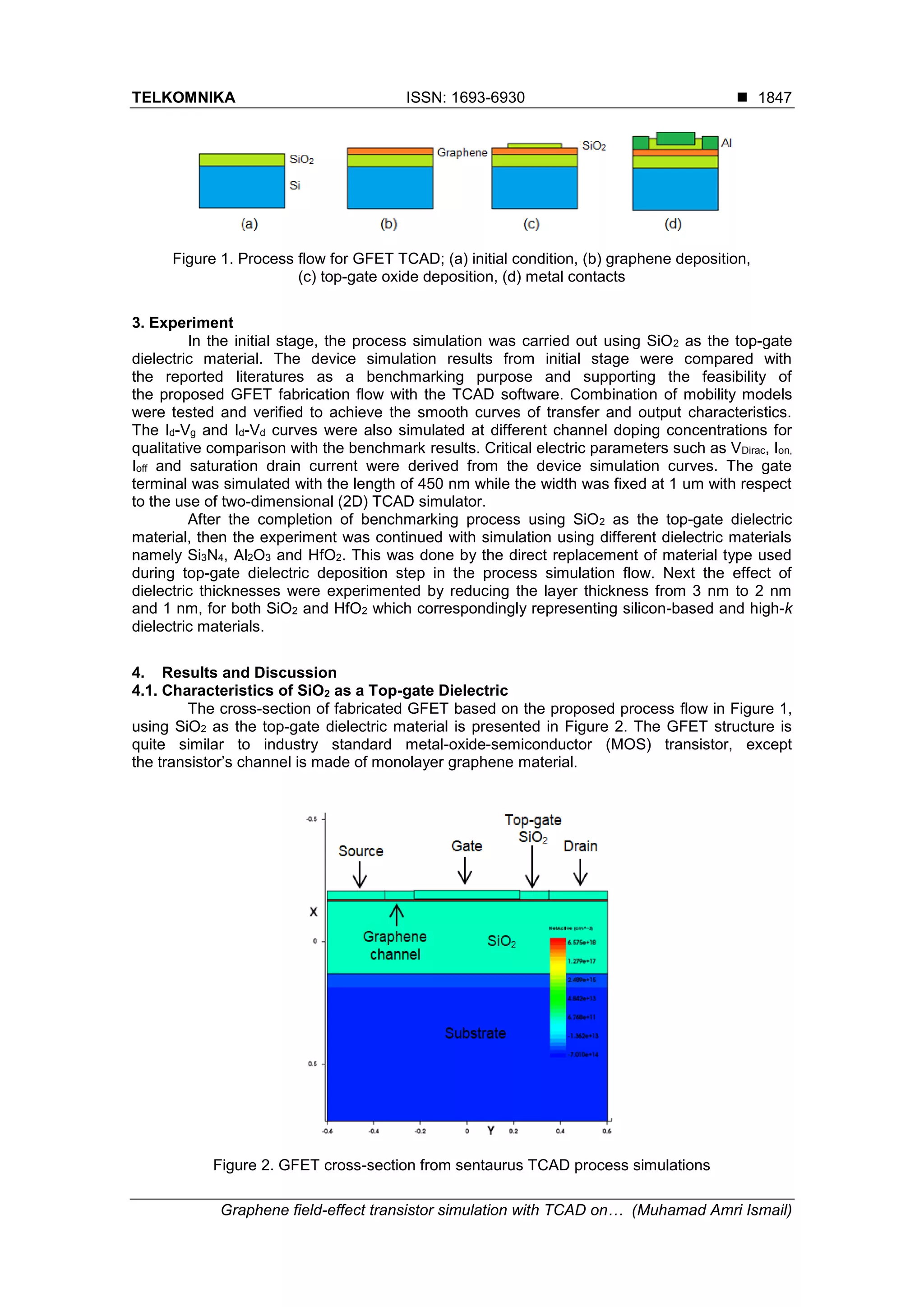
In mimicking the complete GFET fabrication flow, Sentaurus TCAD software from
Synopsys was utilized in this work as it contains both process and device simulations [20]. For
process simulation, there are several fabrication steps involved as simplified in Figure 1.
The initial condition is a p-type boron-doped silicon at 1x1015 cm-3 concentration. Next, silicon
dioxide at 300 nm thickness was deposited using diffusion process with dry oxygen at 1000 ĖC
for 880 minutes. After that, graphene layer was deposited at 5 nm thickness. From typical
process simulation point of view, graphene is not a standard material offered by any TCAD
software hence polysilicon was chosen as transistorās channel region for this work. As
polysilicon is not a self-doping layer while graphene layer is, arsenic at 5x1015 cm-3
concentration was doped to the polysilicon layer to represent such effect. Then, 3 nm thickness
of silicon dioxide was diffused and aligned accordingly to gate structure on top of the graphene
layer to represent the GFETās top-gate dielectric layer. For the contact formation, 35 nm
thickness of aluminum (Al) was deposited and aligned to the contact mask.
Modification of standard polysilicon material properties is mandatory to really represent
the actual monolayer graphene properties to the transistorās channel. For this purpose,
particularly with the use of Sentaurus TCAD process platform, several material parameters are
involved namely bandgap, carrier mobility, permittivity ratio of graphene and vacuum as well
constant mobility, as proposed by Ciarrocchi [21]. For the device time-dependent simulation,
the selection of suitable transport models is crucial in order to find the right combination for both
recombination and carrier mobility models. In Sentaurus TCAD device simulation, recombination
phenomenon is modelled with standard Shockley Read Hall (SRH) model while there are
several carrier mobility models available such as Philips unified mobility (PhuMob), high field
saturation and normal electric field (Enormal) [22]. Good model combinations are required to get
the smooth transfer characteristic curves especially at the VDirac region which is the transition
from hole to electron conductions.
3. TELKOMNIKA ISSN: 1693-6930 ļ®
Graphene field-effect transistor simulation with TCAD onā¦ (Muhamad Amri Ismail)
1847
Figure 1. Process flow for GFET TCAD; (a) initial condition, (b) graphene deposition,
(c) top-gate oxide deposition, (d) metal contacts
3. Experiment
In the initial stage, the process simulation was carried out using SiO2 as the top-gate
dielectric material. The device simulation results from initial stage were compared with
the reported literatures as a benchmarking purpose and supporting the feasibility of
the proposed GFET fabrication flow with the TCAD software. Combination of mobility models
were tested and verified to achieve the smooth curves of transfer and output characteristics.
The Id-Vg and Id-Vd curves were also simulated at different channel doping concentrations for
qualitative comparison with the benchmark results. Critical electric parameters such as VDirac, Ion,
Ioff and saturation drain current were derived from the device simulation curves. The gate
terminal was simulated with the length of 450 nm while the width was fixed at 1 um with respect
to the use of two-dimensional (2D) TCAD simulator.
After the completion of benchmarking process using SiO2 as the top-gate dielectric
material, then the experiment was continued with simulation using different dielectric materials
namely Si3N4, Al2O3 and HfO2. This was done by the direct replacement of material type used
during top-gate dielectric deposition step in the process simulation flow. Next the effect of
dielectric thicknesses were experimented by reducing the layer thickness from 3 nm to 2 nm
and 1 nm, for both SiO2 and HfO2 which correspondingly representing silicon-based and high-k
dielectric materials.
4. Results and Discussion
4.1. Characteristics of SiO2 as a Top-gate Dielectric
The cross-section of fabricated GFET based on the proposed process flow in Figure 1,
using SiO2 as the top-gate dielectric material is presented in Figure 2. The GFET structure is
quite similar to industry standard metal-oxide-semiconductor (MOS) transistor, except
the transistorās channel is made of monolayer graphene material.
Figure 2. GFET cross-section from sentaurus TCAD process simulations
4. ļ® ISSN: 1693-6930
TELKOMNIKA Vol. 17, No. 4, August 2019: 1845-1852
1848
The simulated transfer characteristic using different combination of mobility models are
presented in Figure 3. The results show that the combination of Philips unified (PhuMob) and
high field saturation models provide the smoothest curves as compared to other combinations.
The inclusion of Enormal mobility model generally contributed to the unnecessary kink effect at
the VDirac point. Therefore only PhuMob and high field saturation models are selected for mobility
models while SRH is used for recombination model for the rest of this work.
Figure 4 shows the ambipolar characteristics of Id-Vg curves for GFET with SiO2 as a
top-gate dielectric material, biased at different drain voltage (Vd). Based on this TCAD
simulation works, the most significant graphene properties are the bandgap and carrier mobility
where the former is particularly producing the ambipolar curves valid from negative to positive
gate voltage (Vg) while the latter is imperative for symmetrical shape of the transfer
characteristic curves. It is observed that both Ion and Ioff increase with the increased of Vd while
both VDirac and Ion/Ioff values remain unchanged.
Besides that, Ion is decreases with the increased of doping concentration of channelās
region as shown in Figure 5 for Vd = 0.2 V. There is a shift of the VDirac, from -0.72 V to -0.60 V
respectively for the doping concentration of 1x1015 cm-3 and 1x1019 cm-3, which is supporting
the idea of tuning the GFET polarity by amending graphene concentration level at certain
values [23]. Both outcome of Figure 4 and 5 are critical as benchmarking purposes which are
consistent with the results obtained by Johirul et al [9]. The sensitivities of graphene material to
voltage and doping concentration variations further promoted its suitability to be well qualified
for sensor applications [11].
Figure 3. Transfer characteristic curves from
different combinations of mobility models
Figure 4. Transfer characteristic curves at
different drain voltages (Vd)
Figure 5. Transfer characteristic curves at different channel doping concentrations
5. TELKOMNIKA ISSN: 1693-6930 ļ®
Graphene field-effect transistor simulation with TCAD onā¦ (Muhamad Amri Ismail)
1849
The drain current as a function of drain voltage with different channel doping
concentrations and gate voltages is presented in Figure 6. The simulated results show that
saturation drain current decreases with increasing channel doping concentration. On
the contrary, the saturation drain current increases with increasing biased gate voltage.
These results are also qualitatively comparable with the reported data by Johirul and Thingujam
et al [14, 15]. It is worth noting that hydrodynamic model is included during the simulation of
output characteristic curves in order to increase the accuracies. It slightly increased
the simulation time but necessary for normal Id-Vd curves, or else the fast and simple model
simulations end up with unnecessary resistor characteristics.
Figure 6. Output characteristic curves at different channel doping concentrations
4.2. GFET Simulations at Various Top-gate Dielectric Materials
The transfer characteristic curves of SiO2, Si3N4, Al2O3 and HfO2 as the top-gate
dielectric material at film thickness of 3 nm are illustrated in Figure 7 (a). The maximum Ion is
about 121 uA by using HfO2 followed by Al2O3 and Si3N4 as the experimental materials
respectively at 118 uA and 117 uA. The lowest Ion produced from initial benchmark material of
SiO2 at about 114 uA, which is 6% lower compared to the highest Ion value. The results show
that the Ion value increases with the use of high-k top-gate dielectric material where both HfO2
and Al2O3 are superior as compared to silicon-based dielectric of Si3N4 and SiO2. Besides that
the use of high-k dielectric material also leads to the positive shift of VDirac from -0.72 V using
SiO2 to -0.48 V using HfO2. Both Si3N4 and Al2O3 though shared same VDirac at -0.54 V.
Interestingly all of the top-gate dielectric materials generated about the same value of Ioff at
99 uA to make the ratio of Ion/Ioff increased from 1.15 of SiO2 to 1.18, 1.19 and 1.22
correspondingly to Si3N4, Al2O3 and HfO2. These results exhibit that the use of HfO2 is the best
option for the overall improvement to the critical electrical parameters such as Ion and ratio
of Ion/Ioff.
The output characteristic curves of various top-gate dielectric materials used during
device simulation experimentations are depicted in Figure 7 (b). Consistent with transfer
characteristic curves of Figure 7 (a), the Id-Vd plot also shows that HfO2 yielded the highest
saturation drain current while SiO2 produced the lowest saturation drain current. Based on these
simulated curves, about 12% improvement of saturation drain current can be observed by
replacing the top-gate dielectric material from SiO2 to HfO2. These results agree well with
current graphene-based transistorās engineering towards the use of high-k dielectric material for
better device performance [24]. With respect to this distinguished comparison between SiO2 and
HfO2, the rest of comparisons are done based on these two dielectric materials.
6. ļ® ISSN: 1693-6930
TELKOMNIKA Vol. 17, No. 4, August 2019: 1845-1852
1850
(a) (b)
Figure 7. Simulation curves at various top-gate dielectric materials:
(a) transfer characteristic and (b) output characteristics
4.3. GFET Simulations at Different Top-gate Dielectric Thicknesses
Figure 8 (a) and 8 (b) show the result of device simulations using SiO2 respectively for
transfer and output characteristic curves at different top-gate dielectric thicknesses. For Id-Vg
plot, there is a consistent increase of Ion when the dielectric thickness reduced from 3 nm to
2 nm and 1 nm. The results show that Ion improves by 6% to 121 uA, as the thickness is
reduced to 1 nm. There is also a shift of VDirac observed from -0.72 V to -0.6 V and -0.48 V when
the thickness reduced from 3 nm to 2 nm and 1 nm accordingly. Furthermore, the ratio of Ion/Ioff
increases about 6% with reduction of top-gate dielectric thickness from the minimum of 1.15 to
the maximum of 1.22 as constant Ioff value extracted even at different dielectric thicknesses
applied. For Id-Vd plot, the results show that the saturation drain current increases with reduction
of dielectric thickness, which is consistent with Id-Vg plot.
Figure 9 (a) and 9 (b) illustrate correspondingly the Id-Vg and Id-Vd characteristics with
HfO2 as the top-gate dielectric material at different dielectric thicknesses. It is seen that Ion is
slightly increases with the reduction of dielectric thickness for Id-Vg curves while the saturation
drain current rises by 5% to 4.85 mA as the thickness is decreased from 3 nm to 1 nm for Id-Vd
curves. The overall results of HfO2 simulations are harmonious with previous SiO2 results which
exhibit both silicon-based and high-k dielectric materials produce better electrical parameters
with the decreasing of dielectric thickness. These attainments also match well with
contemporary GFET development in the vicinity of an ultra-thin dielectric material [25].
(a) (b)
Figure 8. Simulation curves at different top-gate dielectric thicknesses for SiO2:
(a) transfer characteristics and (b) output characteristics
7. TELKOMNIKA ISSN: 1693-6930 ļ®
Graphene field-effect transistor simulation with TCAD onā¦ (Muhamad Amri Ismail)
1851
(a) (b)
Figure 9. Simulation curves at different top-gate dielectric thicknesses for HfO2:
(a) transfer characteristics and (b) output characteristics
5. Conclusion
The improvement to the saturation drain current and ratio of Ion/Ioff for GFET
characteristics were successfully evaluated using TCAD simulations under varying top-gate
dielectric materials and thicknesses. The high-k dielectric material has been investigated where
the replacement of SiO2 to HfO2 shows an improvement in saturation drain current about 12%.
The outcomes also reveal that the replacement to HfO2 improves the ratio of Ion/Ioff about 6%
compared to SiO2. For the variations of dielectric thickness, the ratio of Ion/Ioff increased by about
6% when dielectric thickness was reduced from 3 nm to 1 nm for SiO2 material, which provides
option for silicon-based dielectric refinement. These consequences are precious for the process
engineers in determining the suitable top-gate dielectric material with related thickness for
actual process fabrications with respect to the available optimized recipes and equipment.
References
[1] Geim AK, Novoselov KS. The Rise of Graphene. Nature Materials. 2007; 6(3): 183-191.
[2] Geim AK. Graphene: Status and Prospects. Science. 2009; 324(5934): 1530-1534.
[3] Hancock Y. The 2010 Nobel Prize in Physics-Ground-breaking Experiments on Graphene. Physics
D: Applied Physics. 2011; 44(47): 1-12.
[4] Choi W, Lahiri I, Seelaboyina R, Kang YS. Synthesis of Graphene and Its Applications: A Review.
Critical Reviews in Solid State and Material Sciences. 2010; 35(1): 52-71.
[5] Kuila T, Bose S, Mishra AK, Khanra P, Kim NH, Lee JH. Chemical Functionalization of Graphene
and Its Applications. Progress in Materials Science. 2012; 57(7): 1061-1105.
[6] Reddy D, Register LF, Carpenter D, Banerjee SK. Graphene Field-Effect Transistor. Physics D:
Applied Physics. 2011; 44(31): 1-12.
[7] Anteroinen J. Structure and Electrical Characteristics of Graphene Field Effect Transistors. Master
Thesis. Espoo: Aalto University; 2011.
[8] Schwierz F. Graphene Transistors. Nature Nanotechnology. 2010; 5(10): 487-496.
[9] Vaziri S, Lupina G, Henkel C, Smith AD, Ostling M, Dabrowski J, Lippert G, Mehr W, Lemme MC. A
Graphene-based Hot Electron Transistor. Nano Lett. 2013; 13(4): 1435-1439.
[10] Petrone N, Meric I, Hone J, Shepard KL. Graphene Field-Effect Transistors with Gigahertz-frequency
Power Gain on Flexible Substrate. Nano Lett. 2013; 13(1): 121-125.
[11] Zhan B, Li C, Yang J, Jenkins G, Huang W, Dong X. Graphene Field-Effect Transistor and Its
Application for Electronic Sensing. Small. 2014; 10(20): 1-24.
[12] Blom A, Stokbro K. Towards Realistic Atomic-Scale Modeling of Nanoscale Devices. IEEE
International Conference on Nanotechnology. Portland. 2011; 1487-1492.
[13] Hafsi B, Boubaker A, Ismail N, Kalboussi A, Lmimouni K. TCAD Simulations of Graphene Field-Effect
Transistors Based on Quantum Capacitance Effect. Korean Physical Society. 2015; 67(7):
1201-1207.
[14] Johirul M, Sami R, Islam MS, Chowdhury MIB. Study of Characteristics Curves Top-Gated Graphene
FET Using Silvaco TCAD. Electronic Design Engineering. 2017; 3(3): 1-9.
8. ļ® ISSN: 1693-6930
TELKOMNIKA Vol. 17, No. 4, August 2019: 1845-1852
1852
[15] Thingujam T, Jolson K, Kumar M, Sarkar SK. TCAD Based Modeling and Simulation of Graphene
Nanostructured FET (GFET) for High Frequency Performance. Engineering Technology. 2017;
6(1): 1-5.
[16] Shostachenko SA, Zakharchenko RV, Zebrev GI, Stanishevkiy YM, Kargin NI. Dielectric Influence on
IV curve of Graphene Field Effect Transistor. International Conference on Micro-and
Nano-Electronics. Zvenigorod. 2016: 1-5.
[17] Kundu P, Yadav R. Effect of High-K Dielectric Materials on Leakage Current. Electronics and
Computer Science Engineering. 2009; 1(3): 1454-1458.
[18] Lemme MC, Echtermeyer TJ, Baus M, Kurz H. A Graphene Field Effect Device. IEEE Electron
Device Letters. 2007; 28(4): 282-284.
[19] Meric I, Han MY, Young AF, Ozyilmaz B, Kim P, Shepard KL. Current Saturation in Zero-bandgap,
Top-Gated Graphene Field-Effect Transistors. Nature Nanotechnology. 2008; 3(11): 654-659.
[20] Pandit S. Study of Deep Sub-Micron VLSI MOSFET through TCAD. In: Sarkar CK. Editors.
Technology Computer Aided Design: Simulation for VLSI MOSFET. 1st ed. Boca Raton: CRC Press;
2013: 237-266.
[21] Ciarrocchi A. Graphene and 2D Materials for Radiation Detection Devices. Master Thesis. Pisa:
University of Pisa; 2016.
[22] Nier O. Development of TCAD Modeling for Low Field Electronics Transport and Strain Engineering
in Advanced Fully Depleted Silicon on Insulator (FDSOI) CMOS Transistors. PhD Thesis. Grenoble:
Universite Grenoble Alpes; 2015.
[23] Li H, Zhang Q, Liu C, Xu S, Gao P. Ambipolar to Unipolar Conversion in Graphene Field-Effect
Transistors. ACS Nano. 2011; 5(4): 3198-3203.
[24] Zou X, Huang CW, Wang L, Yin LJ, Li W, Wang J, Wu B, Liu Y, Yao Q, Jiang C, Wu WW, He L,
Chen S, Ho Jc, Liao L. Dielectric Engineering of a Boron Nitride/Hafnium Oxide Heterostructure for
High-Performance 2D Field Effect Transistor. Advanced Materials. 2016; 28(10): 2062-2069.
[25] Xiao M, Qiu C, Zhang Z, Peng LM. Atomic-Layer-Deposition Growth of Ultra-Thin HfO2 Film on
Graphene. ACS Appl. Mater. Interfaces. 2017; 9(39): 34050-34056.