S-1
Supporting Information
Wafer-scale Fabrication of Nitrogen-doped Reduced Graphene Oxide with
Enhanced Quaternary-N for High-Performance Photodetection
Muhammad Aniq Shazni Mohammad Haniff1, *, Nur Hamizah Zainal Ariffin2, Syed Muhammad
Hafiz3, Poh Choon Ooi4, Mohd Ismahadi Syono1, Abdul Manaf Hashim2
1Advanced Devices Lab, MIMOS Berhad, Technology Park Malaysia, 57000 Kuala Lumpur,
Malaysia
2Advanced Devices and Materials Engineering Research Lab, Department of Electronic Systems
Engineering, Malaysia-Japan International Institute of Technology, Universiti Teknologi Malaysia,
54100 Kuala Lumpur, Malaysia
3Materials Synthesis & Characterization Laboratory, Institute of Advanced Technology, Universiti
Putra Malaysia, 43400 UPM Serdang, Malaysia
4Institute of Microengineering and Nanoelectronics, Universiti Kebangsaan Malaysia, 43600 Bangi,
Malaysia
*Corresponding author: E-mail address: aniq.haniff@mimos.my (M.A.S.M. Haniff)
Keywords: Nitrogen-doped reduced graphene oxide; quaternary-N; plasma treatment; wafer-scale
fabrication; photodetector
S-2
1) Morphology of N-rGO nanosheets at different plasma power and time
Additional experiments have been carried out in order to further investigate the surface morphology
of N-rGO nanosheets at different plasma power and time at 700 ˚C. Fig. S1(a-c) showed the FESEM
images of the surface morphology for the as-annealed rGO nanosheets in vacuum for 10 min, plasma-
treated N-rGO nanosheets at 20 W for 10 min, and the plasma-treated N-rGO nanosheets at 50 W for
3 min. Fig. S1(a) revealed that few-layers graphene sheets in random stacking order are clearly visible
on the substrate surface. After the plasma treatment at 20 W for a prolonged time of 10 min, the high-
visibility of layer-by-layer graphene sheets completely turned to the continuous film with uniform
dark color contrast (see Fig. S1(b)). Here, we believed that some carbon deposition and nitrogen
doping were taken place on the surface and the resultant N-rGO nanosheets are expected to become
much thicker compared to the as-annealed rGO nanosheets. As for the plasma-treated N-rGO
nanosheets at a higher power of 50 W for 3 min, we found that the large and uneven voids were
apparently formed on the substrate due to the substantial destructive etching effect of the plasma (see
Fig. S1(c)).
Figure S1: FESEM images of (a) as-annealed rGO nanosheets in vacuum atmosphere for 10 min, (b)
plasma-treated N-rGO nanosheets at 20 W for 10 min and (c) plasma-treated N-rGO nanosheets at 50
W for 3 min. The temperature, chamber pressure and gas flowrate for C2H2 and NH3 are kept constant
at 700 C, 2.0 mbar and 10 sccm and 40 sccm, respectively.
S-3
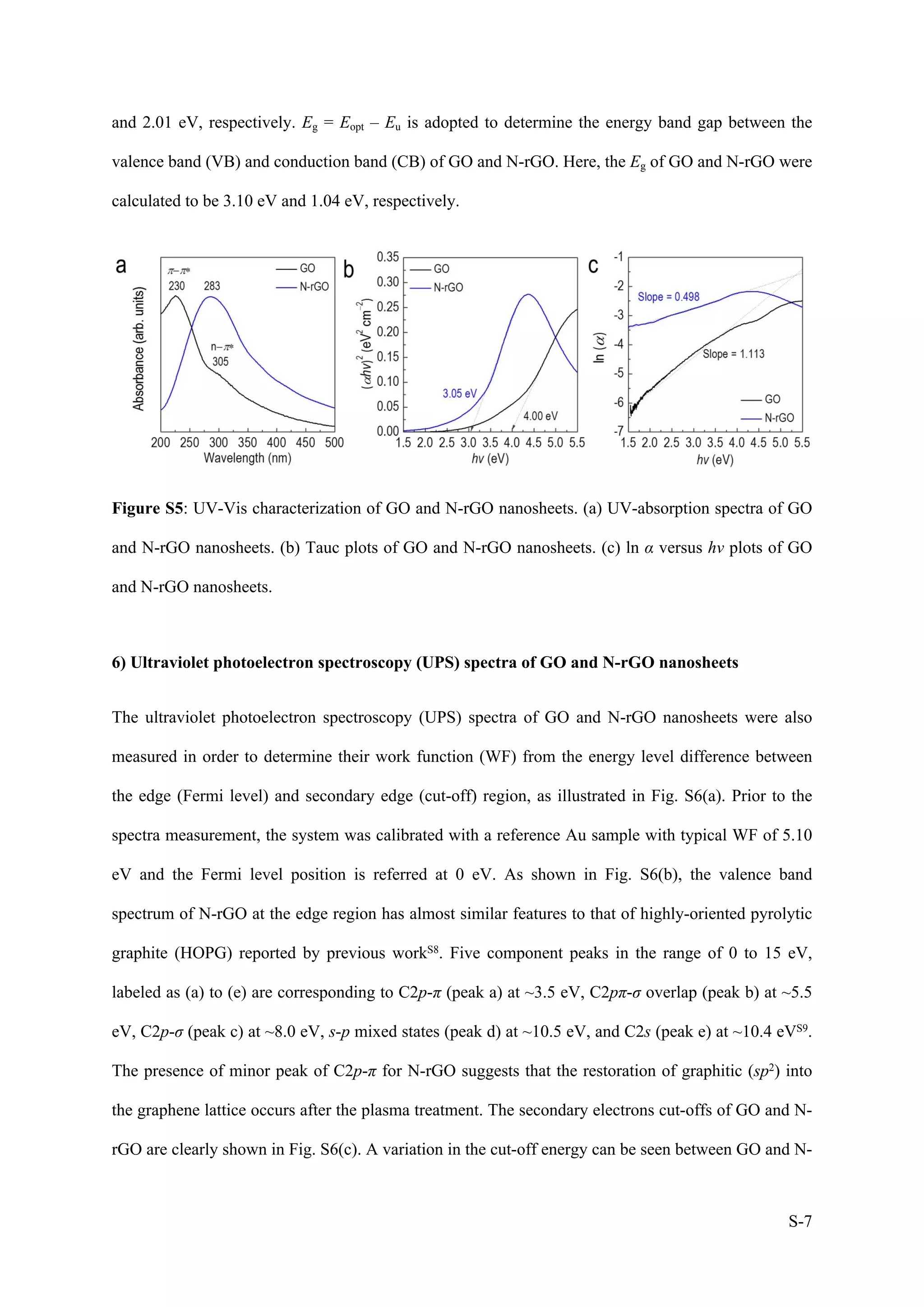
2) Atomic structure of N-rGO nanosheets
The atomic structure of N-rGO nanosheets incorporated onto the device structure was characterized
by high-resolution transmission electron microscopy (HR-TEM). Fig. S2(a) displayed a low
magnification bright field TEM image of N-rGO nanosheets, illustrating few layers with few wrinkles
and crumped balls after the plasma treatment. These features are possibly attributed to the variation of
thermal expansion coefficient (TEC) between GO and the substrate due to rapid heating or cooling as
discussed in the literatureS1. In the Fig. S2(b), HR-TEM image on the selected yellow area showed
quadrilaterals like shaped of few layers graphene where the graphene domains seem to be oriented
randomly with rotational stacking fault. This rotation was further confirmed by its corresponding FFT
pattern, as shown in the inset of Fig. S2(b), which revealed a clear ring shaped consisting of many
diffraction spots. Furthermore, this stacking nature of graphene layers can be also seen through SAED
characterization, as shown in Fig. S2(c). Here, we observed multiple hexagonal rings of different spot
intensities along [001] axis, confirming the presence of rotational stacking fault in the N-rGO
nanosheets. The interplanar distances were determined to be ~0.25 nm and ~0.14 nm corresponding to
the (100) and (110) planes, respectively.
Figure S2: Atomic structure of N-rGO nanosheets. (a) TEM image of N-rGO nanosheets with
wrinkles and crumpled balls formation. The yellow triangles indicate the crumpled balls. (b) HR-
TEM image of N-rGO nanosheets. The inset shows the FFT pattern on the selected yellow square
area. (c) SAED image of N-rGO nanosheets observed along the [001] zone axis.
S-4
3) XPS spectra of N-rGO nanosheets by NH3 plasma treatment
The N-rGO nanosheets were prepared by rapid thermal annealing at 700˚C under vacuum pressure of
1 × 10⁻⁴ mbar for 30 min, followed by NH3 plasma treatment with at a flow rate of 50 sccm, chamber
pressure of 2.0 mbar and plasma power of 20 W for 3 min. The N-rGO nanosheets were then
characterized using XPS to evaluate the surface elemental composition, as shown in Fig. S3(a). The
N-rGO nanosheets showed the presence of main C 1s, N 1s and O 1s peak located around 284 eV, 399
eV, and 531 eV, respectively. Here, the C/O atomic ratio was determined to be 4.52, which is slightly
higher than that of GO (1.81). The increased C/O atomic ratio in the N-rGO implies the removal of
oxygen functional groups and the restoration of sp2 hybridized carbon domains after the plasma
treatment. Next, the C 1s peak was deconvoluted into its respective components which can be
assigned to C=C sp2, N-sp2 hybridized C, C-O, N-sp3 hybridized C, C=O and O-C=O bonds at 284.8
eV, 286.1 eV, 286.4 eV, 287.3 eV, 288.1 eV and 289.3 eV, respectively, as shown in Fig. S3(b). On
the other hand, N 1s was also deconvoluted into its respective components which can be assigned to
pyridinic-N, pyrrolic-N and quaternary-N at 398.5 eV, 400.1 eV and 401.3 eV, respectively, as shown
in Fig. S3(c). Here, the N doping into the graphene lattice was found to be at 1.85at.% with major
content of pyridinic-N, which is in good agreement with the findings reported in previous workS2.
Figure S3: Surface elemental composition of the N-rGO nanosheets by NH3 plasma treatment. (a)
Survey scan XPS spectra of N-rGO nanosheets. (b) High-resolution C 1s and (c) N 1s spectra of N-
rGO nanosheets. The components under C 1s and N 1s are obtained by curve-fitting method.
S-5
4) Structural analysis of GO, rGO, and N-rGO nanosheets by Raman spectra measurements
Raman spectra measurements was employed to investigate structural properties of GO, rGO and N-
rGO nanosheets and the results are shown in Fig. S4(a). Two typical peaks of D and G band were
displayed at about 1356 cm-1 and 1601 cm-1, respectively. Here, the G peak represents the ordered
graphite corresponding to the first-order scattering of the E2g phonon in graphene while the D peak
represents the disordered graphite associated with defects and amorphous carbonS3. A much higher
intensity of the D band was apparently observed for the rGO after rapid annealing in vacuum
atmosphere at 700˚C in comparison to that of GO. In general, the intensity ratio of the D to G band
(ID/IG) illustrates a direct measure of defects or disorder degree in the graphitic materialsS4. In this
case, the ID/IG ratio obtained from the as-annealed rGO spectrum was estimated to be about 1.43,
which significantly increased relative to the bare GO by about 1.04. Here, the increase of ID/IG ratio is
commonly explained as a decrease in the average crystallite size but an increase in the number of sp2
hybridized carbon domains upon the rapid thermal reduction. It should be noted that the rapid
annealing process can damage the graphene structures by creating imperfections and vacancies
because of the substantial reduction in the mass of the GO. Therefore, the presence of more isolated
graphene domains is suggested in the rGO compared to the bare GO. Meanwhile, after plasma
treatment in C2H2-NH3 atmosphere, we found that the intensity of the D band became much weaker
compared to that of rGO and the ID/IG ratio was about 1.14. This observation suggests the effective
healing of defects in the N-rGO by simultaneous recovery of sp2 hybridized carbon bonds and
substitutional of N atoms into the graphitic basal plane, thus resulting in a lower ID/IG ratio compared
to the rGO. We also further evaluated the disorder degree by determine the defects density of
graphene given byS4: nd = ((1.8 ± 0.5) × 1022)·λ-4·(ID/IG) where λ is the laser excitation wavelength.
The results of nd for the GO, rGO and N-rGO nanosheets are shown in Fig. S4(b).
S-6
Figure S4: Structural analysis of GO, rGO, and N-rGO nanosheets by Raman spectra measurements.
(a) Raman spectra and (b) defect density of GO, r-GO, and N-rGO nanosheets on a SiO2/Si substrate.
The laser excitation wavelength is 473 nm. The rGO nanosheets were prepared by rapid thermal
annealing at 700C under vacuum pressure of 1 × 10⁻⁴ mbar for 30 min.
5) Ultraviolet (UV)-absorption spectra of GO and N-rGO nanosheets
To evaluate the energy level of the GO and N-rGO nanosheets, the UV-absorption spectra of both
samples were measured as shown in Fig. S5(a). After the plasma treatment with C2H2-NH3, a
significant red shift of the π-π* transition peak of C=C bonds can be apparently seen from 230 nm to
283 nm, while a broad shoulder of n-π* transition at 305 nm disappears in the N-rGO, suggesting the
removal of oxygen functional groups and restoration of sp2 conjugated structureS5. Based on the
absorption spectra data, the optical band gap (Eopt) of GO and N-rGO can be estimated from Tauc
plots using the following equationS6: (αhv)2 ∝ (hv – Eopt), where α is the absorption spectra coefficient
and hv is the proton energy. The values of Eopt have been estimated by taking the intercept from the
fitting of the (αhv)2 − hv plots at (αhv)2 = 0, as shown in Fig. S5(b), giving an estimated Eopt of GO
and N-rGO to be 4.0 eV and 3.05 eV, respectively. Noted that the band broadening in highly
disordered GO and N-rGO, resulting from the sp2 clusters induced localized states commonly
contributes to the existence of Urbach tail, where the width of Urbach tail (Eu) is governed by α = α0
exp (hv/Eu) in electronic absorptionS7. Fig. S5(c) shows the ln α − hv plots of GO and N-rGO
nanosheets and the Eu as reciprocal value of the slope of the fitting curve is estimated to be 0.90 eV
S-7
and 2.01 eV, respectively. Eg = Eopt – Eu is adopted to determine the energy band gap between the
valence band (VB) and conduction band (CB) of GO and N-rGO. Here, the Eg of GO and N-rGO were
calculated to be 3.10 eV and 1.04 eV, respectively.
Figure S5: UV-Vis characterization of GO and N-rGO nanosheets. (a) UV-absorption spectra of GO
and N-rGO nanosheets. (b) Tauc plots of GO and N-rGO nanosheets. (c) ln α versus hv plots of GO
and N-rGO nanosheets.
6) Ultraviolet photoelectron spectroscopy (UPS) spectra of GO and N-rGO nanosheets
The ultraviolet photoelectron spectroscopy (UPS) spectra of GO and N-rGO nanosheets were also
measured in order to determine their work function (WF) from the energy level difference between
the edge (Fermi level) and secondary edge (cut-off) region, as illustrated in Fig. S6(a). Prior to the
spectra measurement, the system was calibrated with a reference Au sample with typical WF of 5.10
eV and the Fermi level position is referred at 0 eV. As shown in Fig. S6(b), the valence band
spectrum of N-rGO at the edge region has almost similar features to that of highly-oriented pyrolytic
graphite (HOPG) reported by previous workS8. Five component peaks in the range of 0 to 15 eV,
labeled as (a) to (e) are corresponding to C2p-π (peak a) at ~3.5 eV, C2pπ-σ overlap (peak b) at ~5.5
eV, C2p-σ (peak c) at ~8.0 eV, s-p mixed states (peak d) at ~10.5 eV, and C2s (peak e) at ~10.4 eVS9.
The presence of minor peak of C2p-π for N-rGO suggests that the restoration of graphitic (sp2) into
the graphene lattice occurs after the plasma treatment. The secondary electrons cut-offs of GO and N-
rGO are clearly shown in Fig. S6(c). A variation in the cut-off energy can be seen between GO and N-
S-8
rGO due to the modification of atomic structures into the graphene lattice, where the GO tends to cut-
off at a much lower energies of 34.7 eV, while the N-rGO appears to cut-off around 34.95 eV. In
UPS, the WF can be calculated using the relation: ɸ = hv – |Ecut-off – EF|, where hv, Ecut-off, and EF is the
photon energy of Hg (39.5 eV), the cut-off energy and the Fermi energy, respectively. The WF of N-
rGO was calculated to be 4.55 eV, which is much lower than that of GO (4.80 eV). The observation
suggests that the decreased WF is possibly attributed to decrease in the number of electron
withdrawing groups (e.g. -OH, -O-, O=C-O) and increase in the number of electron donating groups
from the main quaternary-N to the carbon network, thus requiring much lower energy to withdraw an
electron completely from the Fermi level. A similar trend of WF for the r-GO attached with additional
electron donating groups was also reported by literaturesS10, S11, suggesting that the work function
tunability in GO structures is possible by controlling the types of dopants.
Figure S6: UPS characterization of GO and N-rGO nanosheets. (a) Survey scan UPS spectra of GO,
N-rGO nanosheets and Au with (b) magnified region near Fermi level and (c) magnified secondary
electron threshold region. The gray-dot arrows denote the values of Ecut-off for the respective GO, N-
rGO and Au. The UPS spectra were calibrated with a reference Au sample with typical WF of 5.10.
7) Dynamic photoresponse of N-rGO device with low quaternary-N
The N-rGO device with low quaternary-N were prepared by rapid thermal annealing at 700˚C under
vacuum pressure of 1 × 10⁻⁴ mbar for 30 min, followed by NH3 plasma treatment with at a flow rate of
50 sccm, chamber pressure of 2.0 mbar and plasma power of 20 W for 3 min. The low content of
quaternary-N in the N-rGO was confirmed by XPS spectra results (see Fig. S3). The dynamic
S-9
photoresponse of the N-rGO device was measured at white-light intensity of 58.1 mW cm−2, as shown
in Fig. S7(a) and (b). The N-rGO device exhibits a stable photoresponse to the “on” and “off”
switching of the beam of light with a relative hysteresis of below ~1%. Here, the time constants for
both rise and decay response were calculated to be ~900 ms, which are slightly longer compared to
that of N-rGO with high quaternary-N. We attribute the longer time constants to the high content of
residual oxygen functional groups in the N-rGO nanosheets (C/O ratio of 4.52).
Figure S7: Dynamic photoresponse of N-rGO device with high pyridinic-N (or low quaternary-N) at
Vbias = 1.0 V and P = 58.1 mW cm−2. (a) Cyclic test of device performance up to 65 cycles. (b) Time-
dependence of current at initial cycle.
8) Photoresponsivity, photodetectivity and external quantum efficiency as a function of laser
power
S-10
Figure S8: Photo-induced response of the N-rGO device under local laser excitation. (a)
Photoresponsivity, (b) photodetectivity and (c) external quantum efficiency as a function of laser
power at 473 nm, 632.8 nm and 785 nm excitation wavelengths.
References
(S1) Yoon, D.; Son, Y. W.; Cheong, H. Negative Thermal Expansion Coefficient of Graphene
Measured by Raman Spectroscopy. Nano Lett. 2011, 11, 3227–3231.
(S2) Li, X.; Wang, H.; Robinson, J.; Sanchez, H.; Diankov, G.; Dai, H. Simultaneous Nitrogen
Doping and Reduction of Graphene Oxide. J. Am. Chem. Soc. 2009, 131, 15939-15944.
(S3) Dresselhaus, M.S.; Jorio, A.; Hofmann, M,; Dresselhaus, G.; Saito, R. Perspective on Carbon
Nanotubes and Graphene Raman Spectroscopy. Nano Lett. 2010, 10(3), 751-758.
(S4) Cançado, L.G.; Jorio, A.; Martins Ferreira, E.H.; Stavale, F.; Achete, C.A.; Capaz, R.B.;
Moutinho, M.V.O.; Lambardo, A.; Kulmala, T.S.; Ferrari, A.C. Quantifying Defects in Graphene
via Raman Spectroscopy at Different Excitation Energies. Nano Lett. 2011, 11(8), 3190–3196.
(S5) Eda, G.; Lin, Y-Y.; Mattevi, C.; Yamaguchi, H.; Chen, H-A.; Chen, I-S.; Chen, C-W.;
Chhowalla, M. Blue Photoluminescence from Chemically Derived Graphene Oxide. Adv. Mater.
2010, 22 (4), 505-509.
(S6) Zheng, F.; Xu, W-L.; Jin, H-D.; Hao, X-T.; Ghiggino, K.P. Charge Transfer from Poly (3-
hexylthiophene) to Graphene Oxide and Reduced Graphene Oxide. RSC Adv. 2015, 5, 89515-89520.
(S7) Mullins, O.C.; Zhu, Y. First Observation of The Urbach Tail in A Multicomponent Organic
System. Appl. Spectrosc. 1992, 46, 354-356.
(S8) Sutar, D.S.; Singh, G.; Botcha, V.D. Electronic Structure of Graphene Oxide and Reduced
Graphene Oxide Monolayers. J. Appl. Phys. 2012, 101, 1003103.
(S9) Bianconi, A.; Hagström, S.B.M.; Bachrach, R.Z. Photoemission Studies of Graphite High-energy
Conduction-band and Valence-band States Using Soft-x-ray Synchrotron Radiation Excitation. Phys.
Rev. B. 1977, 16, 5543-5548.
S-11
(S10) Peng, X.; Tang, F.; Copple, A. Engineering The Work function of Armchair Graphene
Nanoribbons Using Strain and Functional Species: A First Principles Study. J. Phys. Condens. Matter
2012, 24, 075501.
(S11) Sygellou, L.; Paterakis, G.; Galiotis, C.; Tasis, D. Work Function Tuning of Reduced Graphene
Oxide Thin Films. J. Phys. Chem. C. 2016, 120, 281-291.

Wafer scale fabrication of nitrogen-doped reduced graphene oxide with enhanced quaternary-n for high-performance photodetection

  • 1.
    S-1 Supporting Information Wafer-scale Fabricationof Nitrogen-doped Reduced Graphene Oxide with Enhanced Quaternary-N for High-Performance Photodetection Muhammad Aniq Shazni Mohammad Haniff1, *, Nur Hamizah Zainal Ariffin2, Syed Muhammad Hafiz3, Poh Choon Ooi4, Mohd Ismahadi Syono1, Abdul Manaf Hashim2 1Advanced Devices Lab, MIMOS Berhad, Technology Park Malaysia, 57000 Kuala Lumpur, Malaysia 2Advanced Devices and Materials Engineering Research Lab, Department of Electronic Systems Engineering, Malaysia-Japan International Institute of Technology, Universiti Teknologi Malaysia, 54100 Kuala Lumpur, Malaysia 3Materials Synthesis & Characterization Laboratory, Institute of Advanced Technology, Universiti Putra Malaysia, 43400 UPM Serdang, Malaysia 4Institute of Microengineering and Nanoelectronics, Universiti Kebangsaan Malaysia, 43600 Bangi, Malaysia *Corresponding author: E-mail address: aniq.haniff@mimos.my (M.A.S.M. Haniff) Keywords: Nitrogen-doped reduced graphene oxide; quaternary-N; plasma treatment; wafer-scale fabrication; photodetector
  • 2.
    S-2 1) Morphology ofN-rGO nanosheets at different plasma power and time Additional experiments have been carried out in order to further investigate the surface morphology of N-rGO nanosheets at different plasma power and time at 700 ˚C. Fig. S1(a-c) showed the FESEM images of the surface morphology for the as-annealed rGO nanosheets in vacuum for 10 min, plasma- treated N-rGO nanosheets at 20 W for 10 min, and the plasma-treated N-rGO nanosheets at 50 W for 3 min. Fig. S1(a) revealed that few-layers graphene sheets in random stacking order are clearly visible on the substrate surface. After the plasma treatment at 20 W for a prolonged time of 10 min, the high- visibility of layer-by-layer graphene sheets completely turned to the continuous film with uniform dark color contrast (see Fig. S1(b)). Here, we believed that some carbon deposition and nitrogen doping were taken place on the surface and the resultant N-rGO nanosheets are expected to become much thicker compared to the as-annealed rGO nanosheets. As for the plasma-treated N-rGO nanosheets at a higher power of 50 W for 3 min, we found that the large and uneven voids were apparently formed on the substrate due to the substantial destructive etching effect of the plasma (see Fig. S1(c)). Figure S1: FESEM images of (a) as-annealed rGO nanosheets in vacuum atmosphere for 10 min, (b) plasma-treated N-rGO nanosheets at 20 W for 10 min and (c) plasma-treated N-rGO nanosheets at 50 W for 3 min. The temperature, chamber pressure and gas flowrate for C2H2 and NH3 are kept constant at 700 C, 2.0 mbar and 10 sccm and 40 sccm, respectively.
  • 3.
    S-3 2) Atomic structureof N-rGO nanosheets The atomic structure of N-rGO nanosheets incorporated onto the device structure was characterized by high-resolution transmission electron microscopy (HR-TEM). Fig. S2(a) displayed a low magnification bright field TEM image of N-rGO nanosheets, illustrating few layers with few wrinkles and crumped balls after the plasma treatment. These features are possibly attributed to the variation of thermal expansion coefficient (TEC) between GO and the substrate due to rapid heating or cooling as discussed in the literatureS1. In the Fig. S2(b), HR-TEM image on the selected yellow area showed quadrilaterals like shaped of few layers graphene where the graphene domains seem to be oriented randomly with rotational stacking fault. This rotation was further confirmed by its corresponding FFT pattern, as shown in the inset of Fig. S2(b), which revealed a clear ring shaped consisting of many diffraction spots. Furthermore, this stacking nature of graphene layers can be also seen through SAED characterization, as shown in Fig. S2(c). Here, we observed multiple hexagonal rings of different spot intensities along [001] axis, confirming the presence of rotational stacking fault in the N-rGO nanosheets. The interplanar distances were determined to be ~0.25 nm and ~0.14 nm corresponding to the (100) and (110) planes, respectively. Figure S2: Atomic structure of N-rGO nanosheets. (a) TEM image of N-rGO nanosheets with wrinkles and crumpled balls formation. The yellow triangles indicate the crumpled balls. (b) HR- TEM image of N-rGO nanosheets. The inset shows the FFT pattern on the selected yellow square area. (c) SAED image of N-rGO nanosheets observed along the [001] zone axis.
  • 4.
    S-4 3) XPS spectraof N-rGO nanosheets by NH3 plasma treatment The N-rGO nanosheets were prepared by rapid thermal annealing at 700˚C under vacuum pressure of 1 × 10⁻⁴ mbar for 30 min, followed by NH3 plasma treatment with at a flow rate of 50 sccm, chamber pressure of 2.0 mbar and plasma power of 20 W for 3 min. The N-rGO nanosheets were then characterized using XPS to evaluate the surface elemental composition, as shown in Fig. S3(a). The N-rGO nanosheets showed the presence of main C 1s, N 1s and O 1s peak located around 284 eV, 399 eV, and 531 eV, respectively. Here, the C/O atomic ratio was determined to be 4.52, which is slightly higher than that of GO (1.81). The increased C/O atomic ratio in the N-rGO implies the removal of oxygen functional groups and the restoration of sp2 hybridized carbon domains after the plasma treatment. Next, the C 1s peak was deconvoluted into its respective components which can be assigned to C=C sp2, N-sp2 hybridized C, C-O, N-sp3 hybridized C, C=O and O-C=O bonds at 284.8 eV, 286.1 eV, 286.4 eV, 287.3 eV, 288.1 eV and 289.3 eV, respectively, as shown in Fig. S3(b). On the other hand, N 1s was also deconvoluted into its respective components which can be assigned to pyridinic-N, pyrrolic-N and quaternary-N at 398.5 eV, 400.1 eV and 401.3 eV, respectively, as shown in Fig. S3(c). Here, the N doping into the graphene lattice was found to be at 1.85at.% with major content of pyridinic-N, which is in good agreement with the findings reported in previous workS2. Figure S3: Surface elemental composition of the N-rGO nanosheets by NH3 plasma treatment. (a) Survey scan XPS spectra of N-rGO nanosheets. (b) High-resolution C 1s and (c) N 1s spectra of N- rGO nanosheets. The components under C 1s and N 1s are obtained by curve-fitting method.
  • 5.
    S-5 4) Structural analysisof GO, rGO, and N-rGO nanosheets by Raman spectra measurements Raman spectra measurements was employed to investigate structural properties of GO, rGO and N- rGO nanosheets and the results are shown in Fig. S4(a). Two typical peaks of D and G band were displayed at about 1356 cm-1 and 1601 cm-1, respectively. Here, the G peak represents the ordered graphite corresponding to the first-order scattering of the E2g phonon in graphene while the D peak represents the disordered graphite associated with defects and amorphous carbonS3. A much higher intensity of the D band was apparently observed for the rGO after rapid annealing in vacuum atmosphere at 700˚C in comparison to that of GO. In general, the intensity ratio of the D to G band (ID/IG) illustrates a direct measure of defects or disorder degree in the graphitic materialsS4. In this case, the ID/IG ratio obtained from the as-annealed rGO spectrum was estimated to be about 1.43, which significantly increased relative to the bare GO by about 1.04. Here, the increase of ID/IG ratio is commonly explained as a decrease in the average crystallite size but an increase in the number of sp2 hybridized carbon domains upon the rapid thermal reduction. It should be noted that the rapid annealing process can damage the graphene structures by creating imperfections and vacancies because of the substantial reduction in the mass of the GO. Therefore, the presence of more isolated graphene domains is suggested in the rGO compared to the bare GO. Meanwhile, after plasma treatment in C2H2-NH3 atmosphere, we found that the intensity of the D band became much weaker compared to that of rGO and the ID/IG ratio was about 1.14. This observation suggests the effective healing of defects in the N-rGO by simultaneous recovery of sp2 hybridized carbon bonds and substitutional of N atoms into the graphitic basal plane, thus resulting in a lower ID/IG ratio compared to the rGO. We also further evaluated the disorder degree by determine the defects density of graphene given byS4: nd = ((1.8 ± 0.5) × 1022)·λ-4·(ID/IG) where λ is the laser excitation wavelength. The results of nd for the GO, rGO and N-rGO nanosheets are shown in Fig. S4(b).
  • 6.
    S-6 Figure S4: Structuralanalysis of GO, rGO, and N-rGO nanosheets by Raman spectra measurements. (a) Raman spectra and (b) defect density of GO, r-GO, and N-rGO nanosheets on a SiO2/Si substrate. The laser excitation wavelength is 473 nm. The rGO nanosheets were prepared by rapid thermal annealing at 700C under vacuum pressure of 1 × 10⁻⁴ mbar for 30 min. 5) Ultraviolet (UV)-absorption spectra of GO and N-rGO nanosheets To evaluate the energy level of the GO and N-rGO nanosheets, the UV-absorption spectra of both samples were measured as shown in Fig. S5(a). After the plasma treatment with C2H2-NH3, a significant red shift of the π-π* transition peak of C=C bonds can be apparently seen from 230 nm to 283 nm, while a broad shoulder of n-π* transition at 305 nm disappears in the N-rGO, suggesting the removal of oxygen functional groups and restoration of sp2 conjugated structureS5. Based on the absorption spectra data, the optical band gap (Eopt) of GO and N-rGO can be estimated from Tauc plots using the following equationS6: (αhv)2 ∝ (hv – Eopt), where α is the absorption spectra coefficient and hv is the proton energy. The values of Eopt have been estimated by taking the intercept from the fitting of the (αhv)2 − hv plots at (αhv)2 = 0, as shown in Fig. S5(b), giving an estimated Eopt of GO and N-rGO to be 4.0 eV and 3.05 eV, respectively. Noted that the band broadening in highly disordered GO and N-rGO, resulting from the sp2 clusters induced localized states commonly contributes to the existence of Urbach tail, where the width of Urbach tail (Eu) is governed by α = α0 exp (hv/Eu) in electronic absorptionS7. Fig. S5(c) shows the ln α − hv plots of GO and N-rGO nanosheets and the Eu as reciprocal value of the slope of the fitting curve is estimated to be 0.90 eV
  • 7.
    S-7 and 2.01 eV,respectively. Eg = Eopt – Eu is adopted to determine the energy band gap between the valence band (VB) and conduction band (CB) of GO and N-rGO. Here, the Eg of GO and N-rGO were calculated to be 3.10 eV and 1.04 eV, respectively. Figure S5: UV-Vis characterization of GO and N-rGO nanosheets. (a) UV-absorption spectra of GO and N-rGO nanosheets. (b) Tauc plots of GO and N-rGO nanosheets. (c) ln α versus hv plots of GO and N-rGO nanosheets. 6) Ultraviolet photoelectron spectroscopy (UPS) spectra of GO and N-rGO nanosheets The ultraviolet photoelectron spectroscopy (UPS) spectra of GO and N-rGO nanosheets were also measured in order to determine their work function (WF) from the energy level difference between the edge (Fermi level) and secondary edge (cut-off) region, as illustrated in Fig. S6(a). Prior to the spectra measurement, the system was calibrated with a reference Au sample with typical WF of 5.10 eV and the Fermi level position is referred at 0 eV. As shown in Fig. S6(b), the valence band spectrum of N-rGO at the edge region has almost similar features to that of highly-oriented pyrolytic graphite (HOPG) reported by previous workS8. Five component peaks in the range of 0 to 15 eV, labeled as (a) to (e) are corresponding to C2p-π (peak a) at ~3.5 eV, C2pπ-σ overlap (peak b) at ~5.5 eV, C2p-σ (peak c) at ~8.0 eV, s-p mixed states (peak d) at ~10.5 eV, and C2s (peak e) at ~10.4 eVS9. The presence of minor peak of C2p-π for N-rGO suggests that the restoration of graphitic (sp2) into the graphene lattice occurs after the plasma treatment. The secondary electrons cut-offs of GO and N- rGO are clearly shown in Fig. S6(c). A variation in the cut-off energy can be seen between GO and N-
  • 8.
    S-8 rGO due tothe modification of atomic structures into the graphene lattice, where the GO tends to cut- off at a much lower energies of 34.7 eV, while the N-rGO appears to cut-off around 34.95 eV. In UPS, the WF can be calculated using the relation: ɸ = hv – |Ecut-off – EF|, where hv, Ecut-off, and EF is the photon energy of Hg (39.5 eV), the cut-off energy and the Fermi energy, respectively. The WF of N- rGO was calculated to be 4.55 eV, which is much lower than that of GO (4.80 eV). The observation suggests that the decreased WF is possibly attributed to decrease in the number of electron withdrawing groups (e.g. -OH, -O-, O=C-O) and increase in the number of electron donating groups from the main quaternary-N to the carbon network, thus requiring much lower energy to withdraw an electron completely from the Fermi level. A similar trend of WF for the r-GO attached with additional electron donating groups was also reported by literaturesS10, S11, suggesting that the work function tunability in GO structures is possible by controlling the types of dopants. Figure S6: UPS characterization of GO and N-rGO nanosheets. (a) Survey scan UPS spectra of GO, N-rGO nanosheets and Au with (b) magnified region near Fermi level and (c) magnified secondary electron threshold region. The gray-dot arrows denote the values of Ecut-off for the respective GO, N- rGO and Au. The UPS spectra were calibrated with a reference Au sample with typical WF of 5.10. 7) Dynamic photoresponse of N-rGO device with low quaternary-N The N-rGO device with low quaternary-N were prepared by rapid thermal annealing at 700˚C under vacuum pressure of 1 × 10⁻⁴ mbar for 30 min, followed by NH3 plasma treatment with at a flow rate of 50 sccm, chamber pressure of 2.0 mbar and plasma power of 20 W for 3 min. The low content of quaternary-N in the N-rGO was confirmed by XPS spectra results (see Fig. S3). The dynamic
  • 9.
    S-9 photoresponse of theN-rGO device was measured at white-light intensity of 58.1 mW cm−2, as shown in Fig. S7(a) and (b). The N-rGO device exhibits a stable photoresponse to the “on” and “off” switching of the beam of light with a relative hysteresis of below ~1%. Here, the time constants for both rise and decay response were calculated to be ~900 ms, which are slightly longer compared to that of N-rGO with high quaternary-N. We attribute the longer time constants to the high content of residual oxygen functional groups in the N-rGO nanosheets (C/O ratio of 4.52). Figure S7: Dynamic photoresponse of N-rGO device with high pyridinic-N (or low quaternary-N) at Vbias = 1.0 V and P = 58.1 mW cm−2. (a) Cyclic test of device performance up to 65 cycles. (b) Time- dependence of current at initial cycle. 8) Photoresponsivity, photodetectivity and external quantum efficiency as a function of laser power
  • 10.
    S-10 Figure S8: Photo-inducedresponse of the N-rGO device under local laser excitation. (a) Photoresponsivity, (b) photodetectivity and (c) external quantum efficiency as a function of laser power at 473 nm, 632.8 nm and 785 nm excitation wavelengths. References (S1) Yoon, D.; Son, Y. W.; Cheong, H. Negative Thermal Expansion Coefficient of Graphene Measured by Raman Spectroscopy. Nano Lett. 2011, 11, 3227–3231. (S2) Li, X.; Wang, H.; Robinson, J.; Sanchez, H.; Diankov, G.; Dai, H. Simultaneous Nitrogen Doping and Reduction of Graphene Oxide. J. Am. Chem. Soc. 2009, 131, 15939-15944. (S3) Dresselhaus, M.S.; Jorio, A.; Hofmann, M,; Dresselhaus, G.; Saito, R. Perspective on Carbon Nanotubes and Graphene Raman Spectroscopy. Nano Lett. 2010, 10(3), 751-758. (S4) Cançado, L.G.; Jorio, A.; Martins Ferreira, E.H.; Stavale, F.; Achete, C.A.; Capaz, R.B.; Moutinho, M.V.O.; Lambardo, A.; Kulmala, T.S.; Ferrari, A.C. Quantifying Defects in Graphene via Raman Spectroscopy at Different Excitation Energies. Nano Lett. 2011, 11(8), 3190–3196. (S5) Eda, G.; Lin, Y-Y.; Mattevi, C.; Yamaguchi, H.; Chen, H-A.; Chen, I-S.; Chen, C-W.; Chhowalla, M. Blue Photoluminescence from Chemically Derived Graphene Oxide. Adv. Mater. 2010, 22 (4), 505-509. (S6) Zheng, F.; Xu, W-L.; Jin, H-D.; Hao, X-T.; Ghiggino, K.P. Charge Transfer from Poly (3- hexylthiophene) to Graphene Oxide and Reduced Graphene Oxide. RSC Adv. 2015, 5, 89515-89520. (S7) Mullins, O.C.; Zhu, Y. First Observation of The Urbach Tail in A Multicomponent Organic System. Appl. Spectrosc. 1992, 46, 354-356. (S8) Sutar, D.S.; Singh, G.; Botcha, V.D. Electronic Structure of Graphene Oxide and Reduced Graphene Oxide Monolayers. J. Appl. Phys. 2012, 101, 1003103. (S9) Bianconi, A.; Hagström, S.B.M.; Bachrach, R.Z. Photoemission Studies of Graphite High-energy Conduction-band and Valence-band States Using Soft-x-ray Synchrotron Radiation Excitation. Phys. Rev. B. 1977, 16, 5543-5548.
  • 11.
    S-11 (S10) Peng, X.;Tang, F.; Copple, A. Engineering The Work function of Armchair Graphene Nanoribbons Using Strain and Functional Species: A First Principles Study. J. Phys. Condens. Matter 2012, 24, 075501. (S11) Sygellou, L.; Paterakis, G.; Galiotis, C.; Tasis, D. Work Function Tuning of Reduced Graphene Oxide Thin Films. J. Phys. Chem. C. 2016, 120, 281-291.