Downloaded 56 times

![CTU: EE 375 – Electronics 1: Lab 3: BJT Amplifier 4
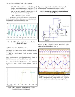
IX. EXPERIMENTAL DATA
The above diagram is the experimental data.
The change in the Vpp voltage alters between 1.35V and 1.38
depending on what resistor values were used. The gain is
approximately 7, according to this result Vpp/.2mV =
1.35/0.2.
X. ANALYSIS/DATA COMPARISON
The analysis/PSpice/Experimental data results were
all accurate, but the results differed between the three. The
reasons that the results were different is because the
experimental results have equipment calibrations, component
tolerances, and actual measures values from the components.
The PSpice results is a close estimate of what the results
showed actually be. For example figure 1 shows a graph of
what the output showed look like. And the actual results
verifies that to be true. The analysis is a good estimate of what
the PSpice results should be. If the PSpice results match the
analysis results, then it’s time to work on the actual lab. All
three were not in total, agreement however, the results were
close to each other, and can be proved by applying the PSpice
Results from Figure 1 to the experimental results.
XI. CONCLUSIONS
The DC Bias values that were calculated by hand are similar
to that of the P-Spice results. The results from the different
methods proves that the P-Spice and hand calculation are
correct.
The measured characteristics closely matched those
in the specifications. A 2N3004 Transistor was used , a
requirement of a gain of 7 was closely achieved because we
obtained a gain of 6.89 from the actual experiment results. The
input resistance that had to be at least 12K was achieved
because the input resistance that we resulted in was
12.9Kohms. The signal was undistorted which is a
requirement for the lab. There was no clipping, or saturation.
Look at figure 5.
This BJT Amplifier lab may be improved to achieve
a closer gain of 7 by altering Rc. Depending on the other
resistor values, whether or not to increase or decrease the
resistance value.
XII. ATTACHMENTS
All figures above follow.
REFERENCES
[1] D. A. Neamen, “Microelectronics: circuit analysis and design - 3rd ed.”
McGraw-Hill, New York, NY, 2007. pp. 1-107.](https://image.slidesharecdn.com/ee375-lab3-120112073301-phpapp01/85/EE375-Electronics-1-lab-3-4-320.jpg)

This lab report examines a BJT amplifier circuit. The objectives were to design the circuit and understand its gain, input/output resistances, and frequency bandwidth. Calculations, PSpice simulations, and experimental results were completed. The calculations, simulations, and experiments all showed similar but not identical results, due to component tolerances and equipment calibration. The final circuit achieved a gain close to the target of 7.

![ppt on IC [Integrated Circuit]](https://cdn.slidesharecdn.com/ss_thumbnails/1-171227170055-thumbnail.jpg?width=640&height=640&fit=bounds)