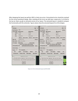
ECE 467 FINAL PROJECT
4 bit synchronous ALU Design
Sidharth Kumar: skumar37@uic.edu (660059012)
Bahareh Pourshirazi: bpours2@uic.edu (665487189)
Dariusz Gorczynski: dgorcz4@uic.edu (671968170)
Vivek Porush: vporus2@uic.edu (663260189)
[Email address]
1
Contents
Figure 1 Two input OR Schematic and Extracted Layout..............................................................................4
Figure 2Two input AND Schematic and Extracted Layout ............................................................................5
Figure 3 Four input Static NOR Schematic and Extracted Layout.................................................................6
Figure 4 Four Input NAND Dynamic Schematic and Extracted Layout .........................................................7
Figure 5 Two input NAND Schematic and Extracted Layout.........................................................................8
Figure 6 Two input Multiplexer Schematic and Extracted Layout................................................................9
Figure 7 An Inverter Schematic and Extracted Layout................................................................................10
Figure 8 Two input XOR Schematic and Extracted Layout for Sum Generation.........................................11
Figure 9 Carry “1” (C1) Schematic and Extracted Layout............................................................................12
Figure 10 Carry “2” (C2) Schematic and Extracted Layout..........................................................................13
Figure 11 Carry “3” (C3) Schematic and Extracted Layout..........................................................................14
Figure 12 Carry “4” (C4) Schematic and Extracted Layout..........................................................................15
Figure 13 Sum Generation of Carry Look Ahead Adder (CAR) Schematic and Extracted Layout ...............16
Figure 14 D Flip Flop Schematic and Extracted Layout for Register ...........................................................17
Figure 15 Multiplexer (6:1) Schematic and Extracted Layout.....................................................................18
Figure 16 Four Bit Register Schematic Extracted Layout for Register ........................................................19
Figure 17 1’s Compliment Schematic and Extracted Layout for Register...................................................20
Figure 18 2’s Compliment Schematic and Extracted Layout for Register...................................................21
Figure 19 Add – Traction Schematic and Extracted Layout ........................................................................22
Figure 20 Final ALU Schematic and Extracted Layout.................................................................................23
Figure 21 LVS on Extracted Layout of OR & AND........................................................................................24
Figure 22 LVS on Extracted Layout of NOR, NAND (2-input), XOR .............................................................25
Figure 23 LVS on Extracted Layout of NAND (4 input), C1, C2....................................................................26
Figure 24 LVS on Extracted Layout of C3, C4 CAR (CLA adder), 4-bit PIPO.................................................27
Figure 25 LVS on Extracted Layout of 1’s & 2’s Compliment, Add-Traction & Multiplexer (6:1) ...............28
Figure 26 LVS on Extracted Layout of final ALU..........................................................................................29
Figure 27 Schematic for test .......................................................................................................................30
Figure 28 Simulation Outputs for “S2 S1 S0” (000) 4-bit Addition Operation............................................31
Figure 29 Simulation Outputs for “S2 S1 S0” (001) 2’s Compliment of “A” Operation ..............................32
Figure 30 Simulation Outputs for “S2 S1 S0” (010) 4-bit Add- Traction Operation....................................33
Figure 31 Simulation Outputs for “S2 S1 S0” (011) 4 input NAND Operation............................................34
Figure 32 Simulation Outputs for “S2 S1 S0” (100) 4-bit NOR Operation..................................................34
Figure 33 Simulation Outputs for “S2 S1 S0” (101) 1’s Compliment ..........................................................35
2
Final-Project
4 bit synchronous ALU Design
6th December 2013
Design Problem:
For the final project we are asked to design a 4-bit synchronous ALU using 250 nm SOI technology.
Moreover, the designed ALU must be able to perform the following functions based on the supplied op-
code:
 4-bit Addition (op-code 000)
 2’s Compliment of A (op. code 001)
 4-bit Add-traction (op. code 010)
 4-input NAND operation using static NAND gate (op. code 011)
 4-input NOR operation using dynamic NOR gate (op. code 100)
 1’s Compliment of B (op. code 101)
The op-codes are supplied on the input line S [3-bit] as “S2 S1 S0”. Based on these op-codes we perform
aforementioned functions on the A [4-bit A3 A2 A1 A0] & B [4-bit B3 B2 B1 B0]. Finally the output is to be
stored in a 4-bit register.
Additional Requirements:
The additional requirements specified for this project are as follows:
 Show the outputs for all possible input combinations.
 Supply Voltage should be specified at 2 Volts.
 Clock frequency should be at least 100 MHz
 The Circuit must drive a load capacitor rated at 10 fF in addition to the parasitic elements, which
are present in the circuit.
 Delay calculations should take into account all the parasitic capacitances in the circuit.

Design Objective:
 The primary objective of this project is to design a functional ALU
 Secondary objective is to perform post-layout
3
Design concept:
As specified by the design guideline, the primary objective is to design a functional ALU. To perform the
specified function we have to build following components:
 2 input OR gate
 2 input AND gate
 4 input NAND gate (Static)
 4 input NOR gate (Dynamic)
 A Carry look ahead adder
 D Flip-Flop
 4-bit Register (PIPO)
 A Multiplexer (6:1)
 1’s Compliment circuit
 2’s Compliment circuit
Moreover we are using the following files as supplied by the TA:
 Final Inverter
 Final Multiplexer (2:1)
Design Schematic and Layout:
The design of the OR, AND, NAND and NOR are straightforward and these components are implemented
as static circuits. These components are designed using pre-defined components “PMOS” & “NMOS” in
the library ‘mitll_fdsoi’. The schematic and extracted layout along with LVS for these components is
shown in the accompanying figures. The values of (W/L) as calculate for symmetric designs are 8 & 4 for
PMOS and NMOS in most of the designs. The D flip-flop and the 4-bit Parallel In Parallel Out register
(PIPO) is positive edge triggered. Core part of our ALU is carry look ahead adder (CLA), which performs
the addition, 2’s compliment and add-traction. We are using a 6:1 Multiplexer to get our final outputs to
the register.
As described in the design problem, based on the select input lines “S2 S1 S0” we perform the required
functions on the input variables and obtain the output on a 4- bit register. To perform NOR & NAND we
have used separate circuits as these have to be performed only on one of the supplied inputs. The NOR
operation is operated on the input “A” and NAND operation is performed on “B”. Similarly, the 1’s
compliment is performed on the input “B”. The outputs from these functions are obtained on the “LSB”
of the 4–bit PIPO register. All the other remaining functions i.e.; 2’s compliment, addition are performed
by Adder (CLA in our project).
All the outputs from these functions are obtained on the 4-bit PIPO register via a 6:1 Multiplexer.
For this part of project we have to create schematic and layout for each component, which then will be
used to create an ALU, using design rules (DRC). We are using a 0.25-micron technology process; all the
components must follow the pre-defined design rules.
4
Figure 1 Two input OR Schematic and Extracted Layout
5
Figure 2Two input AND Schematic and Extracted Layout
6
Figure 3 Four input Static NOR Schematic and Extracted Layout
7
Figure 4 Four Input NAND Dynamic Schematic and Extracted Layout
8
Figure 5 Two input NAND Schematic and Extracted Layout
9
Figure 6 Two input Multiplexer Schematic and Extracted Layout
10
Figure 7 An Inverter Schematic and Extracted Layout
11
Figure 8 Two input XOR Schematic and Extracted Layout for Sum Generation
12
Figure 9 Carry “1” (C1) Schematic and Extracted Layout
13
Figure 10 Carry “2” (C2) Schematic and Extracted Layout
14
Figure 11 Carry “3” (C3) Schematic and Extracted Layout
15
Figure 12 Carry “4” (C4) Schematic and Extracted Layout
16
Figure 13 Sum Generation of Carry Look Ahead Adder (CAR) Schematic and Extracted Layout
17
Figure 14 D Flip Flop Schematic and Extracted Layout for Register
18
Figure 15 Multiplexer (6:1) Schematic and Extracted Layout
19
Figure 16 Four Bit Register Schematic Extracted Layout for Register
20
Figure 17 1’s Compliment Schematic and Extracted Layout for Register
21
Figure 18 2’s Compliment Schematic and Extracted Layout for Register
22
Figure 19 Add – Traction Schematic and Extracted Layout
23
Figure 20 Final ALU Schematic and Extracted Layout
24
After designing the layout we perform DRC to check any errors. Encountered errors should be resolved
for the correct working of design. After resolving all the errors we add input, output pins, Vdd & Gnd to
the lay out. Next, we get an extracted version of our layout. The extracted layout is needed to compare
the functionality with the schematic. Figures above show the extracted layouts for all the designs.
Figure 21 LVS on Extracted Layout of OR & AND
25
Figure 22 LVS on Extracted Layout of NOR, NAND (2-input), XOR
26
Figure 23 LVS on Extracted Layout of NAND (4 input), C1, C2
27
Figure 24 LVS on Extracted Layout of C3, C4 CAR (CLA adder), 4-bit PIPO
28
Figure 25 LVS on Extracted Layout of 1’s & 2’s Compliment, Add-Traction & Multiplexer (6:1)
29
Figure 26 LVS on Extracted Layout of final ALU
Finally in the extracted layout, we perform LVS, which compares and verifies our layout with the
schematic. If LVS is successful a message stating successful LVS is displayed as shown above.
30
Simulation
Using schematic we perform the simulation for the various input functions. VDD is defined as 2V and o/p
capacitance is taken as 10fF. Inputs are connected to voltage sources and vary from 0 - 2V.
Figure 27 Schematic for test
31
1. S2S1S0 = “000”: 4-bit Addition of A and B
Test-1: A = 1111, B = 1111, Out = 1110 (only 4-bits saved)
Test-2: A = 0101, B = 1110, Out = 0011
Figure 28 Simulation Outputs for “S2 S1 S0” (000) 4-bit Addition Operation
Clock
A3
A2
A1
A0
B3
B2
B1
B0
Out3
Out2
Out1
Out0
32
2. S2S1S0 = “001”: 2’s Complement of A
Test 1: A = 1110, Out = 0010 (A’=0001, Out = 0001+1 = 0010)
Test 2: A = 1000, Out = 1000 (A’=0111, Out = 0111+1 = 1000)
Figure 29 Simulation Outputs for “S2 S1 S0” (001) 2’s Compliment of “A” Operation
Clock
A3
A2
A1
A0
Out3
Out2
Out1
Out0
33
3. S2S1S0 = “010”, 4-bit Add-traction of A and B
Test-1: A = 1111, B = 1111, Out = 0000 (Out=A’ + B’ = 0000+0000=0000)
Test-2: A = 0101, B = 1110, Out =1011 (Out=1010+0001=1011)
Figure 30 Simulation Outputs for “S2 S1 S0” (010) 4-bit Add- Traction Operation
A3
A2
A1
A0
B3
B2
B1
B0
Out3
Out2
Out1
Out0
34
4. S2S1S0 = “011”, 4-bit NAND of A (Output is shown on LSB of the Register)
Test 1: 1111 = 0; as the working of NAND suggests, output is 0 only when all bits are high.
Figure 31 Simulation Outputs for “S2 S1 S0” (011) 4 input NAND Operation
Figure 32 Simulation Outputs for “S2 S1 S0” (100) 4-bit NOR Operation
5. S2S1S0 = “100”, 4-bit NOR of A (Output is shown on LSB of the Register)
Test 1: 1111 = 0; as the working of NOR suggests, output is 1 only when all bits are Low.
Clock
A3
A2
A1
A0
Out0
Clock
A3
A2
A1
A0
Out0
35
6. S2S1S0 = “101”, 1’s Complement of B
Test : All bits are reversed as expected
Figure 33 Simulation Outputs for “S2 S1 S0” (101) 1’s Compliment
Result
The 4-bit synchronous ALU was designed using 250 nm SOI technology and the schematic and layout for
all its components was designed and performed successfully. Moreover, as per the design guidelines the
designed ALU is able to perform all the following functions based on the supplied op-code:
 4-bit Addition
 2’s Compliment of “A”
 4-bit Add-traction
 4-input NAND operation
 4-input NOR operation
 1’s Compliment of B
Clock
A3
A2
A1
A0
Out3
Out2
Out1
Out0
36
THANK YOU

ECE_467_Final_Project_Report

  • 1.
    ECE 467 FINALPROJECT 4 bit synchronous ALU Design Sidharth Kumar: skumar37@uic.edu (660059012) Bahareh Pourshirazi: bpours2@uic.edu (665487189) Dariusz Gorczynski: dgorcz4@uic.edu (671968170) Vivek Porush: vporus2@uic.edu (663260189) [Email address]
  • 2.
    1 Contents Figure 1 Twoinput OR Schematic and Extracted Layout..............................................................................4 Figure 2Two input AND Schematic and Extracted Layout ............................................................................5 Figure 3 Four input Static NOR Schematic and Extracted Layout.................................................................6 Figure 4 Four Input NAND Dynamic Schematic and Extracted Layout .........................................................7 Figure 5 Two input NAND Schematic and Extracted Layout.........................................................................8 Figure 6 Two input Multiplexer Schematic and Extracted Layout................................................................9 Figure 7 An Inverter Schematic and Extracted Layout................................................................................10 Figure 8 Two input XOR Schematic and Extracted Layout for Sum Generation.........................................11 Figure 9 Carry “1” (C1) Schematic and Extracted Layout............................................................................12 Figure 10 Carry “2” (C2) Schematic and Extracted Layout..........................................................................13 Figure 11 Carry “3” (C3) Schematic and Extracted Layout..........................................................................14 Figure 12 Carry “4” (C4) Schematic and Extracted Layout..........................................................................15 Figure 13 Sum Generation of Carry Look Ahead Adder (CAR) Schematic and Extracted Layout ...............16 Figure 14 D Flip Flop Schematic and Extracted Layout for Register ...........................................................17 Figure 15 Multiplexer (6:1) Schematic and Extracted Layout.....................................................................18 Figure 16 Four Bit Register Schematic Extracted Layout for Register ........................................................19 Figure 17 1’s Compliment Schematic and Extracted Layout for Register...................................................20 Figure 18 2’s Compliment Schematic and Extracted Layout for Register...................................................21 Figure 19 Add – Traction Schematic and Extracted Layout ........................................................................22 Figure 20 Final ALU Schematic and Extracted Layout.................................................................................23 Figure 21 LVS on Extracted Layout of OR & AND........................................................................................24 Figure 22 LVS on Extracted Layout of NOR, NAND (2-input), XOR .............................................................25 Figure 23 LVS on Extracted Layout of NAND (4 input), C1, C2....................................................................26 Figure 24 LVS on Extracted Layout of C3, C4 CAR (CLA adder), 4-bit PIPO.................................................27 Figure 25 LVS on Extracted Layout of 1’s & 2’s Compliment, Add-Traction & Multiplexer (6:1) ...............28 Figure 26 LVS on Extracted Layout of final ALU..........................................................................................29 Figure 27 Schematic for test .......................................................................................................................30 Figure 28 Simulation Outputs for “S2 S1 S0” (000) 4-bit Addition Operation............................................31 Figure 29 Simulation Outputs for “S2 S1 S0” (001) 2’s Compliment of “A” Operation ..............................32 Figure 30 Simulation Outputs for “S2 S1 S0” (010) 4-bit Add- Traction Operation....................................33 Figure 31 Simulation Outputs for “S2 S1 S0” (011) 4 input NAND Operation............................................34 Figure 32 Simulation Outputs for “S2 S1 S0” (100) 4-bit NOR Operation..................................................34 Figure 33 Simulation Outputs for “S2 S1 S0” (101) 1’s Compliment ..........................................................35
  • 3.
    2 Final-Project 4 bit synchronousALU Design 6th December 2013 Design Problem: For the final project we are asked to design a 4-bit synchronous ALU using 250 nm SOI technology. Moreover, the designed ALU must be able to perform the following functions based on the supplied op- code:  4-bit Addition (op-code 000)  2’s Compliment of A (op. code 001)  4-bit Add-traction (op. code 010)  4-input NAND operation using static NAND gate (op. code 011)  4-input NOR operation using dynamic NOR gate (op. code 100)  1’s Compliment of B (op. code 101) The op-codes are supplied on the input line S [3-bit] as “S2 S1 S0”. Based on these op-codes we perform aforementioned functions on the A [4-bit A3 A2 A1 A0] & B [4-bit B3 B2 B1 B0]. Finally the output is to be stored in a 4-bit register. Additional Requirements: The additional requirements specified for this project are as follows:  Show the outputs for all possible input combinations.  Supply Voltage should be specified at 2 Volts.  Clock frequency should be at least 100 MHz  The Circuit must drive a load capacitor rated at 10 fF in addition to the parasitic elements, which are present in the circuit.  Delay calculations should take into account all the parasitic capacitances in the circuit. 
Design Objective:  The primary objective of this project is to design a functional ALU  Secondary objective is to perform post-layout
  • 4.
    3 Design concept: As specifiedby the design guideline, the primary objective is to design a functional ALU. To perform the specified function we have to build following components:  2 input OR gate  2 input AND gate  4 input NAND gate (Static)  4 input NOR gate (Dynamic)  A Carry look ahead adder  D Flip-Flop  4-bit Register (PIPO)  A Multiplexer (6:1)  1’s Compliment circuit  2’s Compliment circuit Moreover we are using the following files as supplied by the TA:  Final Inverter  Final Multiplexer (2:1) Design Schematic and Layout: The design of the OR, AND, NAND and NOR are straightforward and these components are implemented as static circuits. These components are designed using pre-defined components “PMOS” & “NMOS” in the library ‘mitll_fdsoi’. The schematic and extracted layout along with LVS for these components is shown in the accompanying figures. The values of (W/L) as calculate for symmetric designs are 8 & 4 for PMOS and NMOS in most of the designs. The D flip-flop and the 4-bit Parallel In Parallel Out register (PIPO) is positive edge triggered. Core part of our ALU is carry look ahead adder (CLA), which performs the addition, 2’s compliment and add-traction. We are using a 6:1 Multiplexer to get our final outputs to the register. As described in the design problem, based on the select input lines “S2 S1 S0” we perform the required functions on the input variables and obtain the output on a 4- bit register. To perform NOR & NAND we have used separate circuits as these have to be performed only on one of the supplied inputs. The NOR operation is operated on the input “A” and NAND operation is performed on “B”. Similarly, the 1’s compliment is performed on the input “B”. The outputs from these functions are obtained on the “LSB” of the 4–bit PIPO register. All the other remaining functions i.e.; 2’s compliment, addition are performed by Adder (CLA in our project). All the outputs from these functions are obtained on the 4-bit PIPO register via a 6:1 Multiplexer. For this part of project we have to create schematic and layout for each component, which then will be used to create an ALU, using design rules (DRC). We are using a 0.25-micron technology process; all the components must follow the pre-defined design rules.
  • 5.
    4 Figure 1 Twoinput OR Schematic and Extracted Layout
  • 6.
    5 Figure 2Two inputAND Schematic and Extracted Layout
  • 7.
    6 Figure 3 Fourinput Static NOR Schematic and Extracted Layout
  • 8.
    7 Figure 4 FourInput NAND Dynamic Schematic and Extracted Layout
  • 9.
    8 Figure 5 Twoinput NAND Schematic and Extracted Layout
  • 10.
    9 Figure 6 Twoinput Multiplexer Schematic and Extracted Layout
  • 11.
    10 Figure 7 AnInverter Schematic and Extracted Layout
  • 12.
    11 Figure 8 Twoinput XOR Schematic and Extracted Layout for Sum Generation
  • 13.
    12 Figure 9 Carry“1” (C1) Schematic and Extracted Layout
  • 14.
    13 Figure 10 Carry“2” (C2) Schematic and Extracted Layout
  • 15.
    14 Figure 11 Carry“3” (C3) Schematic and Extracted Layout
  • 16.
    15 Figure 12 Carry“4” (C4) Schematic and Extracted Layout
  • 17.
    16 Figure 13 SumGeneration of Carry Look Ahead Adder (CAR) Schematic and Extracted Layout
  • 18.
    17 Figure 14 DFlip Flop Schematic and Extracted Layout for Register
  • 19.
    18 Figure 15 Multiplexer(6:1) Schematic and Extracted Layout
  • 20.
    19 Figure 16 FourBit Register Schematic Extracted Layout for Register
  • 21.
    20 Figure 17 1’sCompliment Schematic and Extracted Layout for Register
  • 22.
    21 Figure 18 2’sCompliment Schematic and Extracted Layout for Register
  • 23.
    22 Figure 19 Add– Traction Schematic and Extracted Layout
  • 24.
    23 Figure 20 FinalALU Schematic and Extracted Layout
  • 25.
    24 After designing thelayout we perform DRC to check any errors. Encountered errors should be resolved for the correct working of design. After resolving all the errors we add input, output pins, Vdd & Gnd to the lay out. Next, we get an extracted version of our layout. The extracted layout is needed to compare the functionality with the schematic. Figures above show the extracted layouts for all the designs. Figure 21 LVS on Extracted Layout of OR & AND
  • 26.
    25 Figure 22 LVSon Extracted Layout of NOR, NAND (2-input), XOR
  • 27.
    26 Figure 23 LVSon Extracted Layout of NAND (4 input), C1, C2
  • 28.
    27 Figure 24 LVSon Extracted Layout of C3, C4 CAR (CLA adder), 4-bit PIPO
  • 29.
    28 Figure 25 LVSon Extracted Layout of 1’s & 2’s Compliment, Add-Traction & Multiplexer (6:1)
  • 30.
    29 Figure 26 LVSon Extracted Layout of final ALU Finally in the extracted layout, we perform LVS, which compares and verifies our layout with the schematic. If LVS is successful a message stating successful LVS is displayed as shown above.
  • 31.
    30 Simulation Using schematic weperform the simulation for the various input functions. VDD is defined as 2V and o/p capacitance is taken as 10fF. Inputs are connected to voltage sources and vary from 0 - 2V. Figure 27 Schematic for test
  • 32.
    31 1. S2S1S0 =“000”: 4-bit Addition of A and B Test-1: A = 1111, B = 1111, Out = 1110 (only 4-bits saved) Test-2: A = 0101, B = 1110, Out = 0011 Figure 28 Simulation Outputs for “S2 S1 S0” (000) 4-bit Addition Operation Clock A3 A2 A1 A0 B3 B2 B1 B0 Out3 Out2 Out1 Out0
  • 33.
    32 2. S2S1S0 =“001”: 2’s Complement of A Test 1: A = 1110, Out = 0010 (A’=0001, Out = 0001+1 = 0010) Test 2: A = 1000, Out = 1000 (A’=0111, Out = 0111+1 = 1000) Figure 29 Simulation Outputs for “S2 S1 S0” (001) 2’s Compliment of “A” Operation Clock A3 A2 A1 A0 Out3 Out2 Out1 Out0
  • 34.
    33 3. S2S1S0 =“010”, 4-bit Add-traction of A and B Test-1: A = 1111, B = 1111, Out = 0000 (Out=A’ + B’ = 0000+0000=0000) Test-2: A = 0101, B = 1110, Out =1011 (Out=1010+0001=1011) Figure 30 Simulation Outputs for “S2 S1 S0” (010) 4-bit Add- Traction Operation A3 A2 A1 A0 B3 B2 B1 B0 Out3 Out2 Out1 Out0
  • 35.
    34 4. S2S1S0 =“011”, 4-bit NAND of A (Output is shown on LSB of the Register) Test 1: 1111 = 0; as the working of NAND suggests, output is 0 only when all bits are high. Figure 31 Simulation Outputs for “S2 S1 S0” (011) 4 input NAND Operation Figure 32 Simulation Outputs for “S2 S1 S0” (100) 4-bit NOR Operation 5. S2S1S0 = “100”, 4-bit NOR of A (Output is shown on LSB of the Register) Test 1: 1111 = 0; as the working of NOR suggests, output is 1 only when all bits are Low. Clock A3 A2 A1 A0 Out0 Clock A3 A2 A1 A0 Out0
  • 36.
    35 6. S2S1S0 =“101”, 1’s Complement of B Test : All bits are reversed as expected Figure 33 Simulation Outputs for “S2 S1 S0” (101) 1’s Compliment Result The 4-bit synchronous ALU was designed using 250 nm SOI technology and the schematic and layout for all its components was designed and performed successfully. Moreover, as per the design guidelines the designed ALU is able to perform all the following functions based on the supplied op-code:  4-bit Addition  2’s Compliment of “A”  4-bit Add-traction  4-input NAND operation  4-input NOR operation  1’s Compliment of B Clock A3 A2 A1 A0 Out3 Out2 Out1 Out0
  • 37.