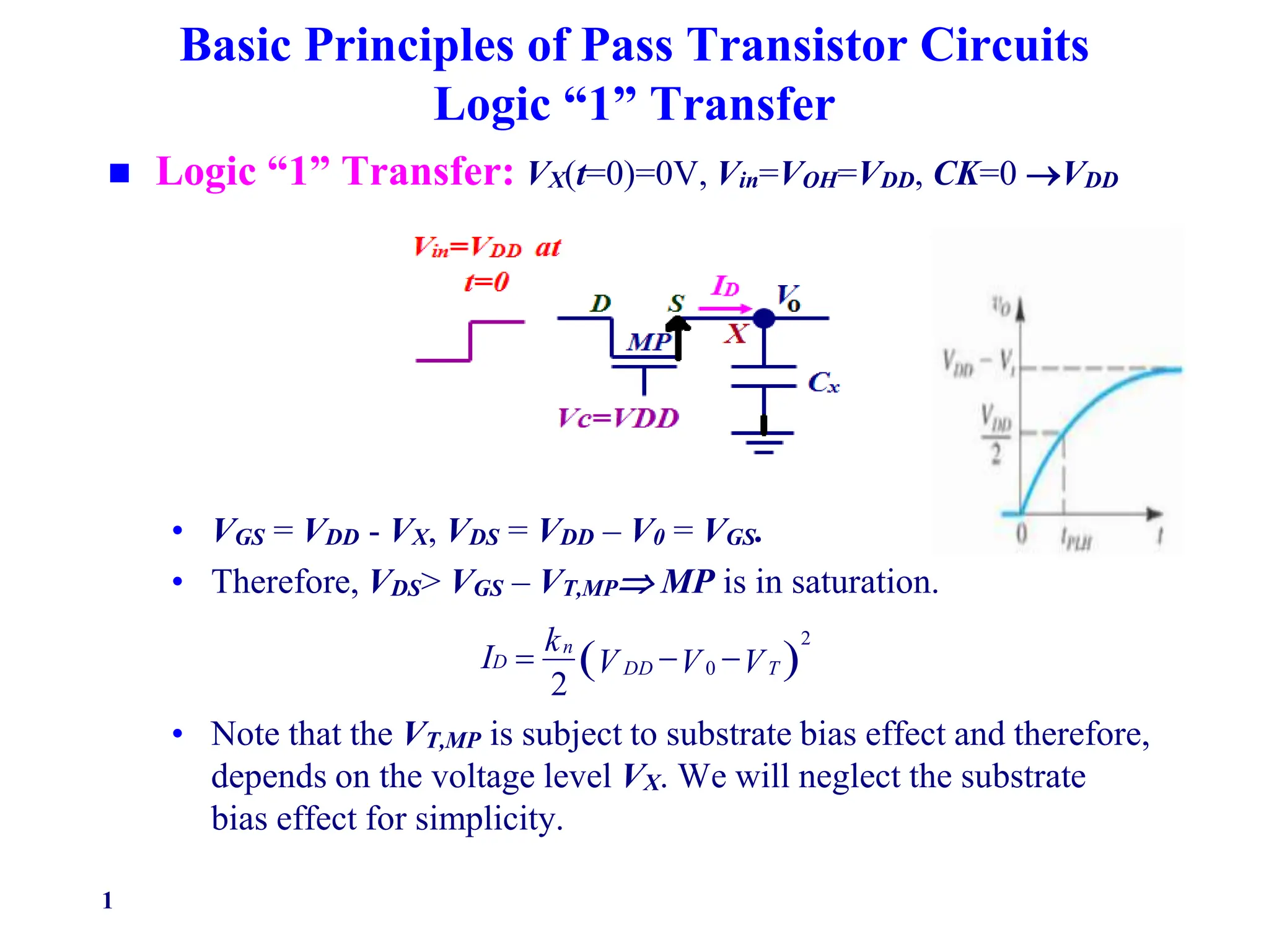
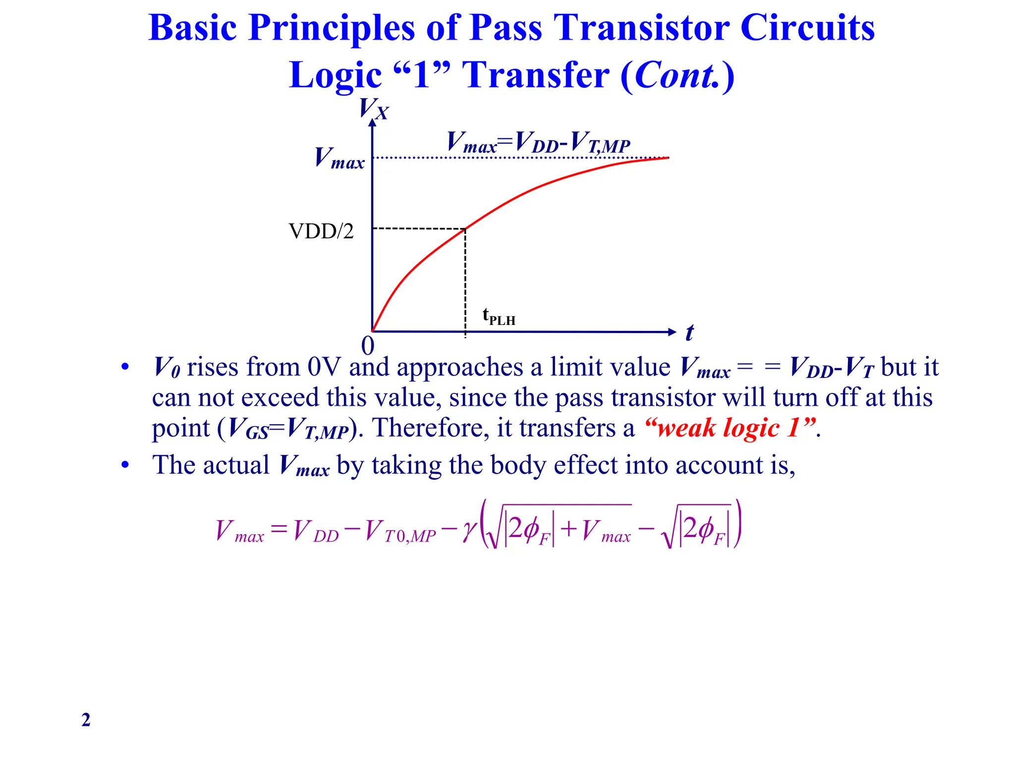
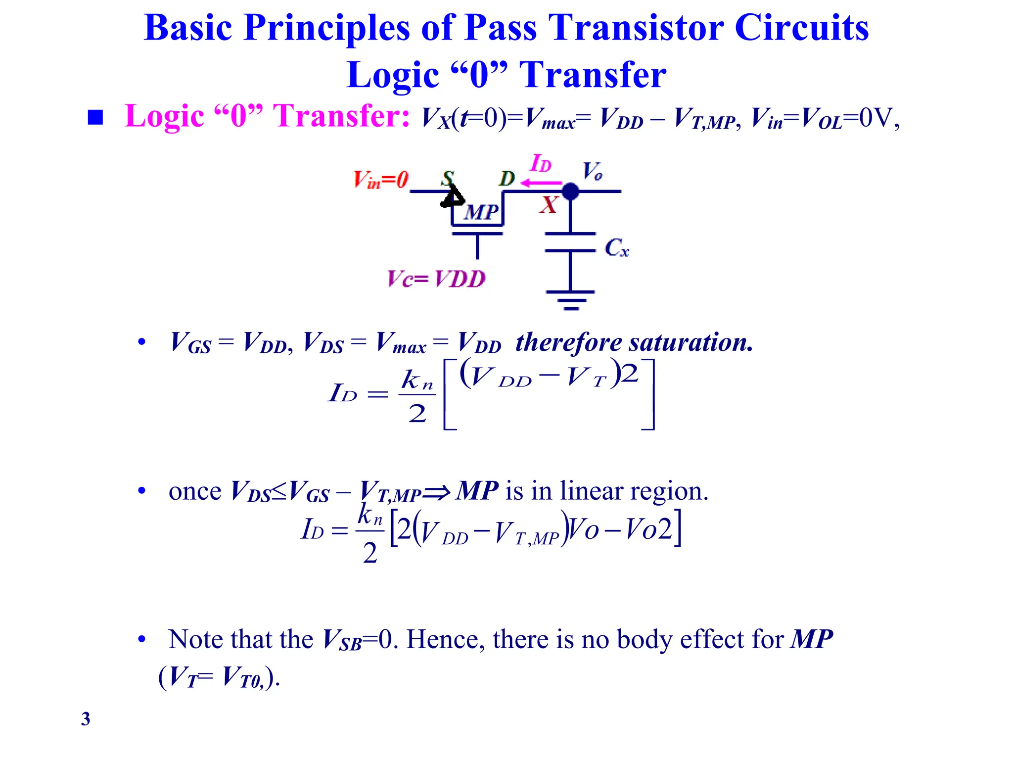
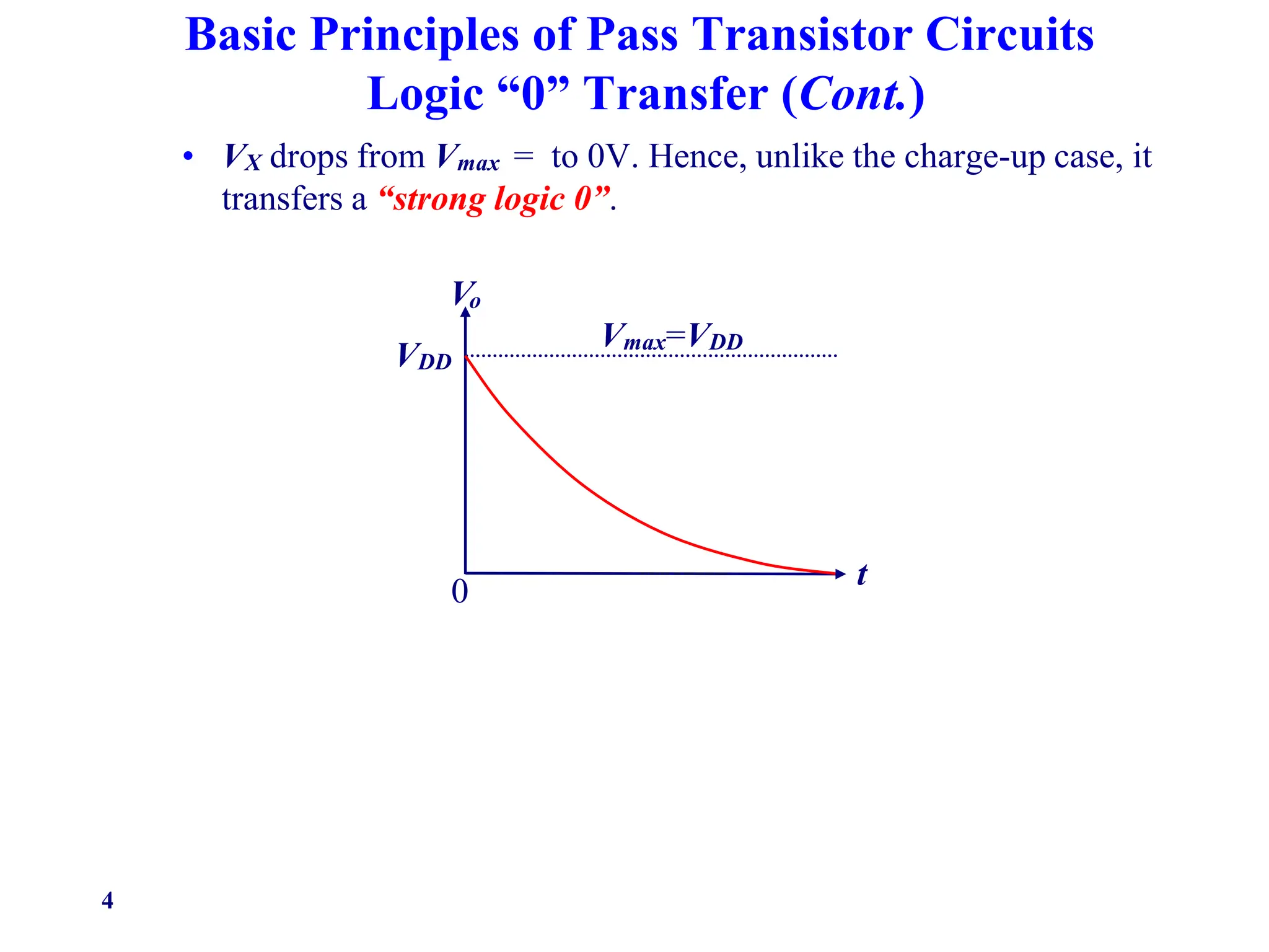
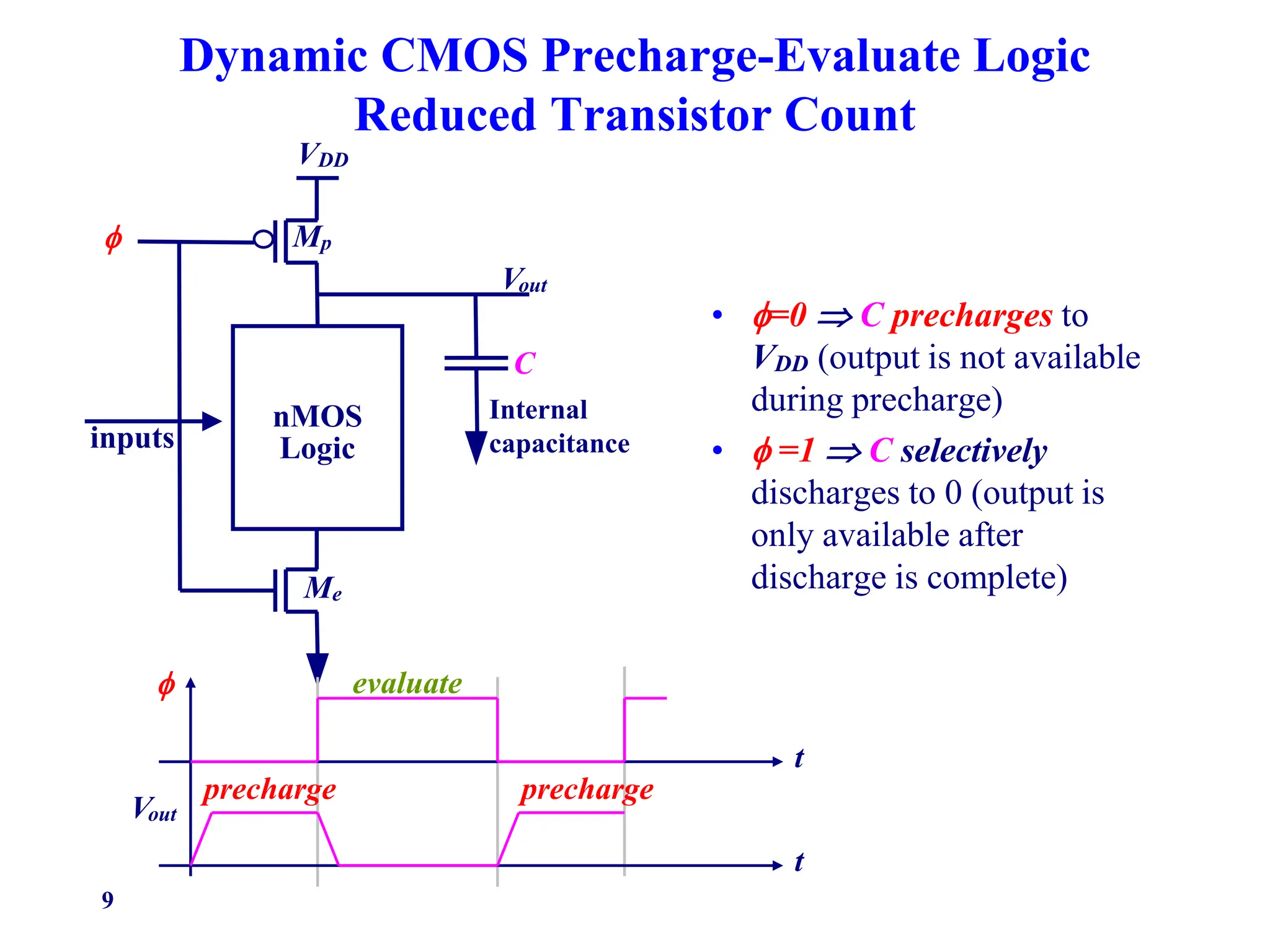
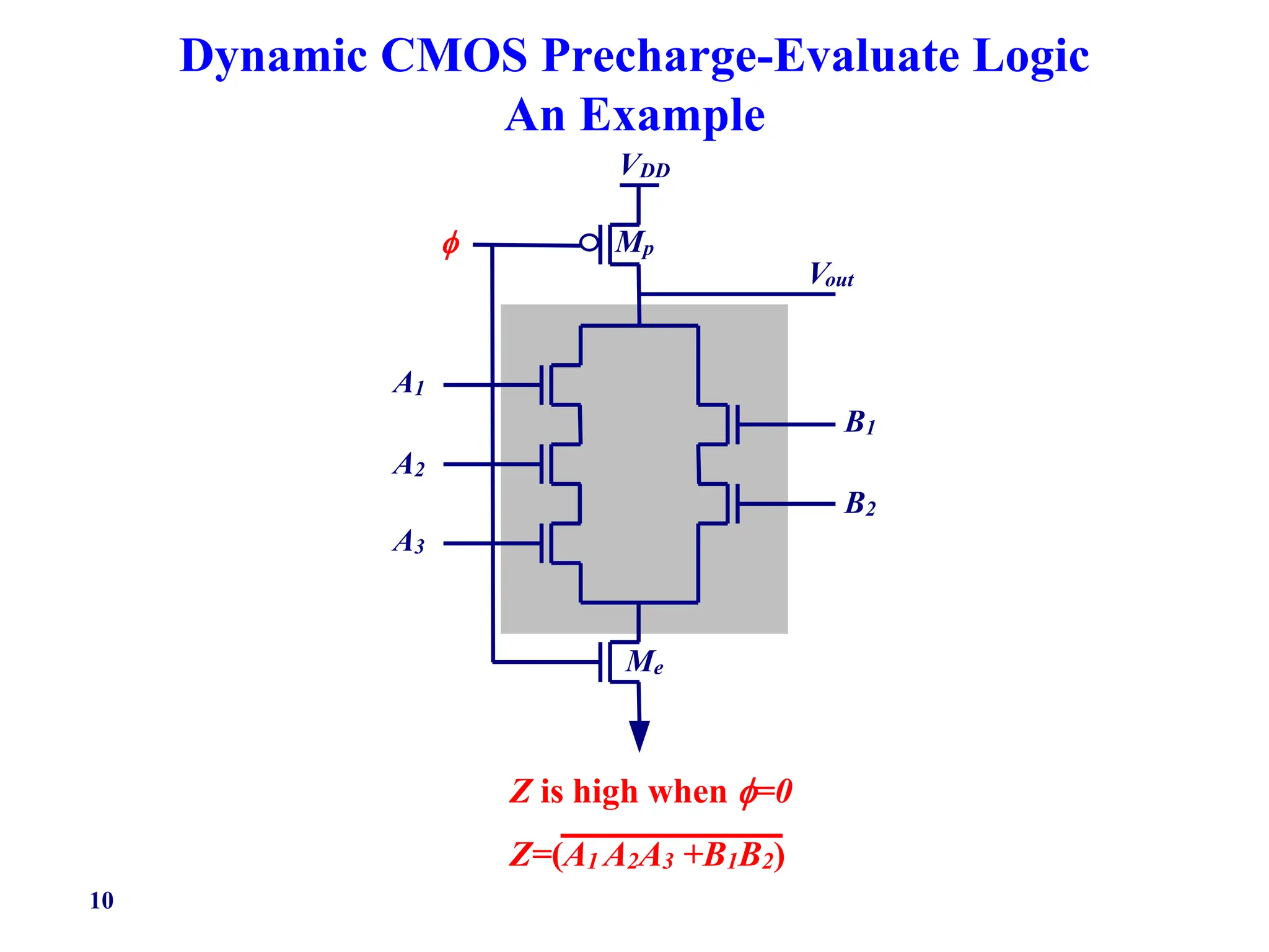
1
Basic Principles of Pass Transistor Circuits
Logic “1” Transfer
 Logic “1” Transfer: VX(t=0)=0V, Vin=VOH=VDD, CK=0 VDD
• VGS = VDD - VX, VDS = VDD – V0 = VGS.
• Therefore, VDS> VGS – VT,MP MP is in saturation.
• Note that the VT,MP is subject to substrate bias effect and therefore,
depends on the voltage level VX. We will neglect the substrate
bias effect for simplicity.
 
V
V
V
k
I T
DD
n
D 

 0
2
2
2
Basic Principles of Pass Transistor Circuits
Logic “1” Transfer (Cont.)
• V0 rises from 0V and approaches a limit value Vmax = = VDD-VT but it
can not exceed this value, since the pass transistor will turn off at this
point (VGS=VT,MP). Therefore, it transfers a “weak logic 1”.
• The actual Vmax by taking the body effect into account is,
 


 2
2
,
0 F
max
F
MP
T
DD
max V
V
V
V 




VX
Vmax
Vmax=VDD-VT,MP
t
0
VDD/2
tPLH
3
Basic Principles of Pass Transistor Circuits
Logic “0” Transfer
 Logic “0” Transfer: VX(t=0)=Vmax= VDD – VT,MP, Vin=VOL=0V,
• VGS = VDD, VDS = Vmax = VDD therefore saturation.
• once VDSVGS – VT,MP MP is in linear region.
• Note that the VSB=0. Hence, there is no body effect for MP
(VT= VT0,).
 
 
2
2
2
, Vo
Vo
V
V
k
I MP
T
DD
n
D 


 





 

2
2
V
V
k
I
T
DD
n
D
4
Basic Principles of Pass Transistor Circuits
Logic “0” Transfer (Cont.)
• VX drops from Vmax = to 0V. Hence, unlike the charge-up case, it
transfers a “strong logic 0”.
Vo
VDD
Vmax=VDD
t
0
Transmission Gates
 The transmission gate utilizes a pair of
complementary transistors connected in parallel.
 It acts as an excellent switch, providing
bidirectional current flow, and it exhibits an
on-resistance that remains almost constant for
wide ranges of input voltage.
 Transmission gate not only an excellent switch in
digital applications but also an excellent analog
switch in such applications as data converters and
switched-capacitor filters
5
TGs……..
Figure a. shows the transmission-gate switch in the "on" position with
the input,Vi, rising to VDD at t = 0.
Assuming, as before, that initially the output voltage is zero, we see that
QN will be operating in saturation and providing a charging current of
6
Transistor QN will conduct a diminishing current that reduces to zero at
V0=VDD-Vtn. Observe, however, that Qp operates with VSG=VDD and is
initially in saturation,
Qp will enter the triode region at VO= | Vtp |, but will continue to conduct
until C is fully charged and VO=VOH=VDD
,
TGs
7
TGs
 QN and QP interchange roles. Analysis of the circuit
in Fig.b.will indicate that QP will cease conduction
when Vo falls to |Vtp|, where |Vtp|is given by
 Transistor QN, however, continues to conduct until C
is fully discharged and Vo= VOL=0V,a "good 0."
8
9
Dynamic CMOS Precharge-Evaluate Logic
Reduced Transistor Count
• =0  C precharges to
VDD (output is not available
during precharge)
•  =1  C selectively
discharges to 0 (output is
only available after
discharge is complete)

VDD
nMOS
Logic
inputs
C
Vout
Me
Mp
Internal
capacitance

t
t
Vout
precharge precharge
evaluate
10
Dynamic CMOS Precharge-Evaluate Logic
An Example

VDD
Vout
Me
Mp
A1
A2
A3
B1
B2
Z is high when =0
Z=(A1 A2A3 +B1B2)
11
Dynamic CMOS Precharge-Evaluate Logic
Advantages/Disadvantages
 Advantages
• Need only N+2 transistors to implement a N-input gate.
• Low static power dissipation
• No DC current paths to place constraints on device sizing
• Input capacitance is same as pseudo nMOS gate.
• Pull-up time is improved by active switch to VDD.
 Disadvantages
• The available time of output is less than 50 % of the time.
• Pull-down time is degraded due to series active switch to 0.
• Logic output value can be degraded due to charge sharing with other gate
capacitances connected to the output.
• Minimum clock rate determined by leakage on C.
• Maximum clock rate determined by circuit delays.
• Input can only change during the precharge phase. Inputs must be stable
during evaluation; otherwise an incorrect value on an input could
erroneously discharge the output node. (single phase P-E logic gates can
not be cascaded)
• Outputs must be stored during precharge, if they are required during the
next evaluate phase.

pass-transistors.ppt working of transistors

  • 1.
    1 Basic Principles ofPass Transistor Circuits Logic “1” Transfer  Logic “1” Transfer: VX(t=0)=0V, Vin=VOH=VDD, CK=0 VDD • VGS = VDD - VX, VDS = VDD – V0 = VGS. • Therefore, VDS> VGS – VT,MP MP is in saturation. • Note that the VT,MP is subject to substrate bias effect and therefore, depends on the voltage level VX. We will neglect the substrate bias effect for simplicity.   V V V k I T DD n D    0 2 2
  • 2.
    2 Basic Principles ofPass Transistor Circuits Logic “1” Transfer (Cont.) • V0 rises from 0V and approaches a limit value Vmax = = VDD-VT but it can not exceed this value, since the pass transistor will turn off at this point (VGS=VT,MP). Therefore, it transfers a “weak logic 1”. • The actual Vmax by taking the body effect into account is,      2 2 , 0 F max F MP T DD max V V V V      VX Vmax Vmax=VDD-VT,MP t 0 VDD/2 tPLH
  • 3.
    3 Basic Principles ofPass Transistor Circuits Logic “0” Transfer  Logic “0” Transfer: VX(t=0)=Vmax= VDD – VT,MP, Vin=VOL=0V, • VGS = VDD, VDS = Vmax = VDD therefore saturation. • once VDSVGS – VT,MP MP is in linear region. • Note that the VSB=0. Hence, there is no body effect for MP (VT= VT0,).     2 2 2 , Vo Vo V V k I MP T DD n D              2 2 V V k I T DD n D
  • 4.
    4 Basic Principles ofPass Transistor Circuits Logic “0” Transfer (Cont.) • VX drops from Vmax = to 0V. Hence, unlike the charge-up case, it transfers a “strong logic 0”. Vo VDD Vmax=VDD t 0
  • 5.
    Transmission Gates  Thetransmission gate utilizes a pair of complementary transistors connected in parallel.  It acts as an excellent switch, providing bidirectional current flow, and it exhibits an on-resistance that remains almost constant for wide ranges of input voltage.  Transmission gate not only an excellent switch in digital applications but also an excellent analog switch in such applications as data converters and switched-capacitor filters 5
  • 6.
    TGs…….. Figure a. showsthe transmission-gate switch in the "on" position with the input,Vi, rising to VDD at t = 0. Assuming, as before, that initially the output voltage is zero, we see that QN will be operating in saturation and providing a charging current of 6 Transistor QN will conduct a diminishing current that reduces to zero at V0=VDD-Vtn. Observe, however, that Qp operates with VSG=VDD and is initially in saturation, Qp will enter the triode region at VO= | Vtp |, but will continue to conduct until C is fully charged and VO=VOH=VDD ,
  • 7.
  • 8.
    TGs  QN andQP interchange roles. Analysis of the circuit in Fig.b.will indicate that QP will cease conduction when Vo falls to |Vtp|, where |Vtp|is given by  Transistor QN, however, continues to conduct until C is fully discharged and Vo= VOL=0V,a "good 0." 8
  • 9.
    9 Dynamic CMOS Precharge-EvaluateLogic Reduced Transistor Count • =0  C precharges to VDD (output is not available during precharge) •  =1  C selectively discharges to 0 (output is only available after discharge is complete)  VDD nMOS Logic inputs C Vout Me Mp Internal capacitance  t t Vout precharge precharge evaluate
  • 10.
    10 Dynamic CMOS Precharge-EvaluateLogic An Example  VDD Vout Me Mp A1 A2 A3 B1 B2 Z is high when =0 Z=(A1 A2A3 +B1B2)
  • 11.
    11 Dynamic CMOS Precharge-EvaluateLogic Advantages/Disadvantages  Advantages • Need only N+2 transistors to implement a N-input gate. • Low static power dissipation • No DC current paths to place constraints on device sizing • Input capacitance is same as pseudo nMOS gate. • Pull-up time is improved by active switch to VDD.  Disadvantages • The available time of output is less than 50 % of the time. • Pull-down time is degraded due to series active switch to 0. • Logic output value can be degraded due to charge sharing with other gate capacitances connected to the output. • Minimum clock rate determined by leakage on C. • Maximum clock rate determined by circuit delays. • Input can only change during the precharge phase. Inputs must be stable during evaluation; otherwise an incorrect value on an input could erroneously discharge the output node. (single phase P-E logic gates can not be cascaded) • Outputs must be stored during precharge, if they are required during the next evaluate phase.